ABSTRACT
STODDARD, NATHAN GREGORY. On the Interactions of Point Defects, Dopants and Light Element Impurities in Silicon as Stimulated by 200 kV Electron Irradiation. (Under the direction of George Rozgonyi and Gerd Duscher.)
The purpose of this research has been the investigation of atomic manipulation in silicon. It has been demonstrated that bulk vacancies and interstitials are created and spatially separated one Frenkel pair at a time during 200 kV electron irradiation of nitrogen-doped silicon. The mechanism by which the nitrogen pair allows Frenkel pair separation is shown to be a combination of the lowering of the energy barrier to a knock-on event
combined with a more stable end-state. Anomalous nitrogen diffusion has been observed as a result of low energy ion milling, and the diffusion of nitrogen is studied theoretically, revealing a new, low energy model for N2 pair diffusion. For the first time, 200 kV irradiation has been demonstrated not only to create Frenkel pairs during broad-beam
irradiation, but also to allow the formation of extended defects like voids, oxygen precipitates and interstitial complexes. Using electron energy loss spectroscopy combined with first principles simulations, dark and bright areas induced in Z contrast images by 200 kV irradiation are demonstrated to be due to vacancy and self-interstitial complexes,
On the Interactions of Point Defects, Dopants and Light Element
Impurities in Silicon as Stimulated by 200 kV Electron Irradiation
by
NATHAN GREGORY STODDARD
A dissertation submitted to the Graduate Faculty of North Carolina State University
in partial fulfillment of the requirements for the Degree of
Doctor of Philosophy
MATERIALS SCIENCE AND ENGINEERING
Raleigh 2004
APPROVED BY:
_____________________ ____________________ _____________________
Dedication
Biography
Acknowledgements
Many people have been helpful to the completion of this body of work, and several have been instrumental. First I would like to acknowledge my colleagues in research: Wolfgang Windl, Abdennaceur Karoui, Fred Stevie, Alex Kvit, Jag Kasichainula, Dawn Bonnell, Rui Shao, and Maxim Nikiforov. I would like to thank my parents, Greg and Teri, for their constant love and support, and I thank my wife, Jen for being my happiness and my lifelong companion. Thank you to my undergraduate research advisor, Joe Schick, for introducing me to the importance of basic scientific research. This work has been supported by the Silicon Wafer Engineering and Defect Science I/U CRC program (grant EEC-9726176) through the National Science Foundation and through the National Renewable Energy Laboratories under contract AAT-2-31605-05. Finally, I would like to acknowledge the members of my thesis committee for their consideration and helpful advice, and especially George Rozgonyi and Gerd Duscher who have been invaluable mentors to me in every way.
Table of Contents
List of Tables……… vii
List of Figures………...……… viii
1 Grand Introduction……….……….. 1
1.1 Current State of the Field………... 1
1.2 Literature Review……….. 3
1.3 Electron-silicon interactions……….. 7
2 Effects of 200 kV electron irradiation on nitrogen doped silicon………… 10
2.1 Materials and Methods………... 10
2.2 Results……… … 11
2.3 Discussion……….. 12
2.4 Conclusion………. 14
3 Nitrogen Pair Diffusion in Silicon………... 15
3.1 Introduction……… 15
3.2 Materials and Methods………... 15
3.3 Results……… 16
3.4 Discussion……….. 18
3.5 Conclusion……… 18
4 Anomalous Nitrogen Diffusion during Ion Milling: a SIMS Study……... 20
4.1 Introduction……… 20
4.2 Materials and Methods………... 21
4.3 Results……… 23
4.5 Conclusion……… 27
5 The Nucleation and Growth of Extended Defects in Silicon from their atomic constituents………...…… 29
5.1 Materials and Methods………...…… 29
5.2 Results………...……. 30
5.3 Discussion………...……… 35
5.4 Conclusion………...……... 42
6 Study of Point Defect Complexes by Electron Energy Loss Spectroscopy and First Principles Simulations………...……... 44
6.1 Introduction……….…..….. 44
6.2 Materials and Methods……… 44
6.3 Results and Discussion……… 46
6.4 Conclusion………... 55
7 The Athermal Manipulation of Dopants to Produce Device Structures on the Nanoscale……… 56
7.1 Introduction………... 56
7.2 Materials and Methods……….. 57
7.3 Results……… 59
7.4 Discussion………. 60
7.5 Conclusion……… 61
List of Tables
1. Bond lengths for diffusion sequences of nitrogen……… 75 2. Summary of nitrogen concentrations after different TEM sample
preparation processes……… 79
3. Maximum energy transfer from a 200 kV electron to atoms
List of Figures
1. Two configurations of nitrogen situated in silicon……….. 67 2. Energy transfer during an elastic e-Si collision as a function of angle…… 68 3. Probability of scattering as a function of imparted energy……….. 68 4. Conventional TEM images of electron irradiated nitrogen-doped and
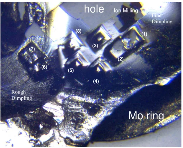
nitrogen-free Czochralski silicon……….. 69 5. Close-up of Fig. 4 with evidence of faceted voids……… 70 6. Z contrast STEM image of irradiated nitrogen-doped CZ-Si………... 70 7. High resolution TEM image of an irradiation induced precipitate………… 71 8. First diffusion path for the nitrogen pair in silicon……… 72 9. Second diffusion path for the nitrogen pair in silicon……… 73 10. Energetics for the diffusion paths of N2……… 74 11. Theoretical and experimental data for the diffusion coefficient of N2 in Si... 75 12. Schematic of surface treatments used in TEM sample preparation………… 76 13. Optical microscope image of a TEM sample prepared as in Fig. 12………. 76 14. SIMS depth profiles of nitrogen in areas of different TEM sample
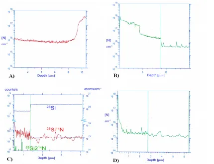
preparation steps……… 77
15. SIMS depth profiles of samples with different ion milling treatments……. 78 16. SIMS depth profile of a sample with a surface nitride removed by ion milling 79 17. N-CZ Si sample after extended broad-beam irradiation with
20. Diffusion path for a silicon atom ejected near a nitrogen pair into a
nearby interstitial position………... 83
21. Energetics for the series illustrated in Fig. 20………. 84
22. Model for electron-beam induced precipitation in N-CZ Si………... 84
23. Cyclical model for the creation of point defects, voids and oxygen precipitates, aided by the nitrogen pair………... 85
24. EELS spectra of interstitial-rich and vacancy-rich regions of irradiated N-FZ Si………. 86
25. High energy resolution EELS spectra of N-FZ Si……… 87
26. Point defects and point defect complexes in silicon………. 88
27. Simulated EELS signals from silicon containing point defects……… 89
28. Simulated EELS signals from silicon containing vacancy complexes……. 90
29. Simulated EELS signals from silicon containing interstitial complexes….. 91
30. Doping profiles of compensated silicon, co-implanted with boron and antimony……… 93
31. Cross-sectional Z contrast images of the near surface of recrystallized implant damage……….. 94
32. Atomic force microscope images of topography and surface potential including one irradiated spot………. 95
33. AFM images of topography and surface potential including a number of irradiated spots……… 96
1 General Introduction 1.1 Current State of Research
Decades of work have created an understanding of the fundamental physics as well as the very successful implementation of engineering techniques to create both efficient solar cells and highly integrated electronic devices. In the field of crystal growth, the key to obtaining highest quality material is control of the point defects and light element impurities incorporated at the solid-melt interface. Once wafers are cut from the ingot, subsequent annealing regimens further tailor the concentration and distribution of larger extended defects that nucleate from smaller grown-in defects. Prime among the extended defects important in single crystal silicon are oxygen precipitates and related stacking faults. Although much is known of the details of the growth process, the nucleation process is still poorly understood. It is believed that nuclei grow one atom at a time, enabled by bulk diffusion at high
temperatures.
individual point defects or complexes of several atoms, so matching experimental to theoretical data has remained elusive.
1.2 Literature Review: nitrogen in silicon and the irradiation of silicon
Among the light element impurities, the use of nitrogen doping in high purity silicon has been a topic of much research in the last few years.6 Both Czochralski (CZ) grown and Float Zone (FZ) processed single crystal silicon benefit in their defect profiles from the introduction of low concentrations (< 1015 cm-3) of nitrogen. Specifically, nitrogen doped CZ silicon (N-CZ Si) has increased denuded zone integrity7 combined with a higher density of smaller oxygen precipitates in the bulk that provide improved gettering ability compared to nitrogen free CZ Si.8 The oxygen precipitate nuclei exist in the as-grown N-CZ Si at a high density, while subsequent precipitate growth rate and size are limited by oxygen diffusion, requiring high temperatures8,9. Theoretical work10 suggests that the split-interstitial N
temperatures.13,14 It has also been shown that the N2 pair readily complexes with vacancies, both in an unstable N2V configuration, and in the very stable N2V2 configuration which can either form from the reaction N2V + V → N2V2 or N2 + V2→ N2V2. The N2V2 complex has further been shown to attract oxygen into a stable configuration, indicating the possibility of further oxygen precipitate nucleation based on the N2 pair.15,16 Schultz and Nelson have discovered a diffusion path for singly occurring interstitial nitrogen involving a pure interstitialcy mechanism.17 A low migration energy diffusion path is demonstrated, going from a threefold-coordinated split interstitial site to a twofold coordinated bridge site and back again, but Schultz and Nelson ignore the N2 pair configuration, which many believe to be the most prevalent nitrogen defect. The diffusion of the nitrogen pair has been considered by Sawada et al., both with simultaneous movement and with sequential movement of the nitrogen atoms, with reported values for the activation barrier of 3.3 and 2.9 eV,
respectively.18 The lower energy barrier agrees well with the experimental value, and moves the nitrogen from the antiparallel ground state to the Humble configuration, both shown in Figure 1, with a second barrier of 1.0 eV to move back into a different antiparallel
founding result of the work presented here demonstrates the creation and separation of Frenkel pairs in nitrogen-doped silicon, but at only 200 kV electron accelerating voltage. Subsequent interaction and complexing of vacancies, self-interstitials and oxygen is also observed by a number of methods.
Much work has also been applied to the simulation of radiation damage and elastic processes. One of the basic parameters of radiation damage is the displacement energy for a material. This can be determined theoretically by finding the saddle point during kick-out of a lattice atom. For silicon, this value depends on the direction in which the atom is knocked, but has been calculated to range from 10-20 eV.26 To accomplish a larger scale modeling of irradiation processes, molecular dynamics simulations are necessary, and have been used to simulate extended defect nucleation and growth. The most recent research has employed multiscale modeling and continuum models to more closely match experimental data on material strength and the dynamics of defect growth.27,28,29
1.3 Electron-Silicon Interactions in a 200 kV TEM
entirety of their momentum to the target atom. Momentum conservation limits the amount of energy that can be transferred, and in the case of a silicon atom, the energy transferred, T, by an electron scattered to an angle θ is
I.)
(
)
2 sin 2
2 2 2
2 θ c m E c m E
T e e
Si
e +
=
where Ee is the electron energy (e.g. 200 keV), c is the speed of light and me is the electron
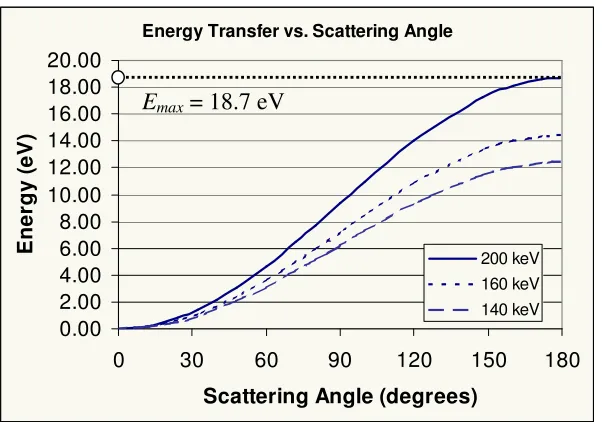
rest mass.30 Using this expression, the maximum possible transferred energy, corresponding to θ = 180, is Tmax = 18.7 eV in a 200 kV TEM. The full plot of transferred energy vs.
scattering angle is given in Fig. 2 for electrons of 140, 160 and 200 keV. The number of
Frenkel pairs, NFP, created from a knock-on collision is described by the modified
Kinchin-Pease expression II.) < ≤ ≤ < = T E E E E T E E T N d d D d d d FP 5 . 2 / 4 . 0 5 . 2 1 0
where T is the imparted energy and Ed is the displacement energy for the material. For
silicon, experiments suggest that Ed ranges from 12-20eV while theoretical studies have
indicated that it might be as low as 10 eV, and depends on the crystallographic
orientation.30,26 For the lowest theoretical values, there have been suggestions that Monte Carlo simulations for longer periods of time result in recombination of the Frenkel pair, so
that the spontaneous recombination volume (SRV) is larger at 300K than ab initio
calculations might predict. If the effective displacement energy is less than 18.6 eV for a
given zone-axis alignment, then one would expect Frenkel pairs to be created during 200kV
10 nm, damage accumulation is not observed. Even though it is commonly quoted that the
minimum TEM beam energy to create Frenkel pairs in Si is 140-160 keV, which corresponds
to a maximum energy transfer of 12.4-14.4eV to silicon, damage is typically only seen under
conditions where the beam is converged to a diameter of ~5nm, at which point a hole can
develop in the thin foil. Another notable exception to the absence of radiation damage is the
use of sample cooling. In an experiment by Yamasaki et al. where the sample temperature
was maintained at 15K, some permanent damage formation became evident after exposure to
a dose of 3*1023/cm2.31 This affirms the earlier conjecture about temperature effects on the
SRV, and suggests that Frenkel pairs are created during the course of 200kV irradiation
under all irradiation conditions; at normal temperatures (300-400K), the Frenkel pairs
recombine soon after the collision, but at low temperatures the damage is frozen in. A
second important conclusion in Yamasaki’s study, agreeing with that of Seidman et al.,32 is that amorphization of silicon is extremely difficult below 1 MeV of accelerating energy, even
at low temperature. Yamasaki and Takeda conclude from this that the introduction of
one-at-a-time Frenkel pairs is insufficient for amorphization, but that damage cascades are the nuclei
for amorphization. This will be revisited based on the results presented below.
To determine the probability of a knock-on collision, one starts with the scattering
cross section. The differential Mott cross section for elastic scattering provides a relativistic
correction to the Rutherford expression as follows33
where Z is atomic number, E is the electron energy, E0 is the electron rest energy, e is the
electron charge, ε0 is the vacuum permittivity, is the scattering angle, α = Z/137 and β =
v/c. The cross-section for imparting at least a given value of energy T( ) (i.e. scattering to
greater than a given scattering angle min) can be derived from the differential cross-section
by integration.
IV.)
( )
( )
Ω = π
θ π θ θ
σ σ
min d 2 sin d
d T
Mott Mott
To translate the cross section into a probability, one can first convert the cross section into an
angle-dependent mean free path.34
V.)
( )
a Mott elastic θ σ n
λ = 1
where na is the number of atoms per unit volume. The probability is then defined by Poisson
statistics in terms of the ratio of the sample thickness, t, to the mean free path.
VI.) t el
el elastic e t t P λ λ θ) / , ( = −
The probability for a collision that transfers energy greater or equal to a given value is plotted
in Fig. 3, so that the probability of a knock-on event can be determined.
This analysis will be used extensively below in an attempt to explain the origin of
many of the 200 kV irradiation effects that are observed. A thorough understanding of the
nature and frequency of electron-silicon interactions is key to the interpretation of the results
to come. This thesis will begin with a number of novel observations dealing with the
electron irradiation of nitrogen-doped silicon in Section 2. In Section 3, a theoretical study
of the diffusion of the nitrogen pair in silicon will be presented where a new, lowest energy
experimentally discovered anomaly in nitrogen diffusion is reported in Section 4, where it is
demonstrated that nitrogen can diffuse over several micrometers in silicon and in the process
build up higher concentrations during low energy, low angle ion milling. This concentration
enhancement is important to an explanation of the electron irradiation effects observed in
N-doped Si, which is provided along with additional experimental data in Section 5. This
section of the thesis also deals with oxygen precipitation, as well as void formation in
low-oxygen nitrogen-doped silicon. In Section 6, the clustering of vacancies and interstitials
during electron irradiation is studied using electron energy loss spectroscopy (EELS) and
supporting theoretical simulations. Section 7 extends the electron-assisted manipulation of
silicon to electronic dopants with fruitful results. Specifically, a method is demonstrated for
2 Effects of 200 kV electron irradiation on nitrogen doped silicon
Published as “In Situ Point Defect Generation and Agglomeration during Electron Beam
Irradiation of Nitrogen-doped Czochralski Silicon”
N. Stoddard, A. Karoui, G. Duscher, A. Kvit and G. Rozgonyi, Electrochemical and Solid
State Letters 6(11) G134-136 (2003).
2.1 Materials and Methods
Three [100] oriented CZ wafers, one from Nippon Steel with [N] = 1x1015cm-3 (measured by secondary ion mass spectroscopy) and two nitrogen-free reference samples,
were prepared for plan view transmission electron microscope (TEM) imaging using
standard methods. A Wacker Siltronic N-free reference sample had an unknown grown-in
vacancy/interstitial prevalence while the other, from MEMC, was grown at the ‘perfect’
Voronkov v/G ratio such that neither intrinsic point defect was predominant35. In a Topcon 002B TEM, all samples were [100] aligned and irradiated under a converged 200 kV electron
beam from a high electron flux LaB6 filament. The converged beam diameter was ~400nm
and irradiation was performed on different areas of the same foil for between 5 and 45
minutes. Analysis by conventional TEM methods was performed in situ in the Topcon
microscope and later in a JEOL 2010F field emission Scanning TEM (STEM) capable of
high resolution (HRTEM), Electron Energy Loss Spectroscopy (EELS) and Z-Contrast
imaging. The Z-Contrast imaging is particularly important in separating atomic number
2.2 Results
Changes in the nitrogen-doped sample were evident after five minutes of irradiation,
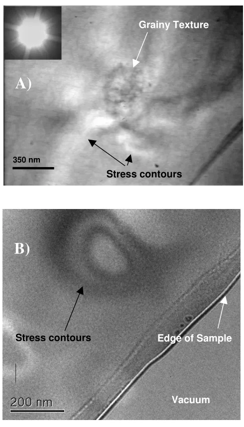
with more dramatic effects appearing after twenty minutes, see Fig. 4A, while the Wacker
N-free reference sample is essentially unchanged under the same conditions, see Fig. 4B. Note
that the grainy texture in the center of Fig. 4A is absent in Fig. 4B, while the stress contrast
lines are much stronger in Fig. 4B. At higher magnification, more details of the grainy
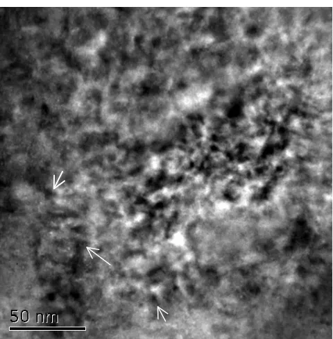
texture in the N-CZ irradiated volume are revealed, see Fig. 5. Dark triangular areas,
indicated by arrows, suggest the formation of faceted voids. A STEM Z-Contrast image, free
from interference due to stress contrast, provides key information about the average atomic
density in Fig. 6. The micrograph shows a dark (i.e. low Z) central region corresponding to
the size of the converged beam, surrounded by a bright ring. Because of the transparency of
Z-contrast image analysis, we may interpret the dark central region to be vacancy-rich, while
the bright surrounding ring is interstitial rich. Some spots of brighter contrast can be seen
within the dark region. They may be clusters of lattice atoms in the vacancy rich region, or
possibly small areas of a second phase with a higher mass density than the rest of the
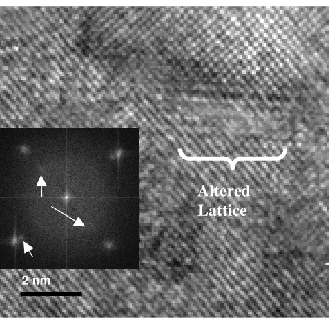
vacancy rich region. Examining the clusters more closely, high-resolution images have
provided some evidence of agglomerated point defects and secondary phases, see Fig. 7,
whose presence is supported by the extra spots in the Fourier transforms. It is possible that
the precipitate-like region may be due to grown-in nitrogen-oxygen precipitates. These
grown-in precipitates should not have high enough volume density for their presence in the
irradiated region to be likely, but the chance cannot be ruled out. Since we have seen several
and none outside, then either the beam interactions are nucleating the clusters or playing a
crucial role in stimulating their growth.
The two N-free reference samples exhibited some subtle differences in response to
the beam. Specifically, we have observed some stress introduced in the Wacker N-free
material, as in Fig 4B, that is absent in the “perfect” MEMC N-free material. This difference
in the response of the reference samples to the e-beam can be explained because, unlike the
MEMC reference that has negligible VSi and SiI concentrations, the Wacker sample was
grown under conditions such that a significant excess of either vacancies or interstitials is
present. This prevailing point defect will diffuse rapidly due to the driving force of the
electron irradiation, even when the lattice is not disturbed. The resulting point defect
concentration gradients in the Wacker sample produce the stress contours that are absent in
the MEMC sample.
2.3 Discussion
These results corroborate the occurrence of Frenkel pair formation during the
interaction of 200 kV electrons with thin foils of silicon. In the N-free samples, the material
shows no signs of the grainy texture present in the N-CZ, see Fig. 4. Since the collision
dynamics are the same, Frenkel pairs must be created in all thin foil Si samples. Normally,
recombination is highly likely, since there is little kinetic energy left over after the knock-on
process. Therefore, without the intervention of nitrogen, there would be no long-range
diffusion or vacancy agglomeration. In the presence of nitrogen, and due to its affinity with
vacancies, the Frenkel pair constituents separate. Once separated, the interstitial atoms
either to the surface, or to an area just outside of the 400nm beam diameter. This causes a
ring of locally higher density, imaged by Z-Contrast as the bright ring seen in Fig. 4, while
the interstitial and vacancy concentration gradients set up the considerable stress seen in Fig.
4A. As for the separation process, it is known that nitrogen forms complexes with vacancies
in the forms of VN, VN2 and V2N2.10 These complexes are nuclei for oxygen precipitation37,
and would be likely to capture vacancies if present immediately after a silicon knock-on
process, thereby preventing recombination with the interstitial and allowing the
self-interstitial to diffuse away. Subsequently, the N-V nuclei could either capture more
vacancies and evolve towards a void, or gather oxygen atoms initiating a SiO2 nucleation
process. The TEM results presented above support this idea, providing evidence for the
presence of both voids (Figs. 5, 6) and nuclei of a second phase (Fig. 7). If the nitrogen can
later separate from the aggregation, then a single N atom (or N2 pair) could initiate multiple
agglomerates over time. Although enough oxygen is present to form significant aggregates,
we do not yet have direct evidence for the presence of oxygen in the observed clusters.
Further experiments and simulation are necessary to elucidate the complex
interactions of VSi, SiI, N and O, particularly since initial calculations indicate that, for a
homogeneous distribution of nitrogen in the material, the dramatic difference in
nitrogen-doped silicon is caused by fewer than ten atoms of nitrogen in the irradiated volume. This is
conceptually problematic, and some alternatives must be considered. First, each nitrogen
atom could be the seed of many extended defects over time. In fact, this is quite probable
since nitrogen tends to segregate to the surface of growing precipitates and voids. However,
believe that the N-doped and N-free wafers are otherwise identical in growth conditions and
doping, and can only conclude that, as in the CZ growth and annealing processes, small
concentrations of nitrogen can have significant effects on material properties.
2.4 Conclusion
The results of this experiment open the interesting possibility of creating a
“laboratory” for performing kinetic studies of intrinsic point defects interacting with N and O
atoms under the electron beam and at room temperature. Observing the formation of point
defect agglomerates under the beam should enhance our understanding of the nucleation of
octahedral voids and oxygen precipitates by sidestepping the experimental constraints of high
3 Nitrogen Pair Diffusion in Silicon
Submitted to Physical Review Letters as “A New, Low Energy Model for Nitrogen Pair
Diffusion in Silicon”, by N. Stoddard, G. Duscher, P. Pichler and W. Windl, July 2004
3.1 Introduction
The current work on modeling nitrogen diffusion was reviewed above. Previous
models for nitrogen diffusion have ignored the N2 paired configuration17 or constrained the
movement based on the requirement of maintaining symmetry12. In this work, the
requirements of symmetry along the diffusion path are dropped, and two new diffusion paths
are identified with calculations that make use of rigorous corrections to the subtleties of the
local density approximation (LDA) and a careful determination of the saddle point. One of
these two paths has a lower activation energy than any previously reported path.
3.2 Materials and Methods
Simulations were performed using the Vienna Ab Initio Simulations Package
(VASP), which employs a self-consistent approach based on density functional theory in the
local density approximation. Ultra-soft pseudopotentials with a plane-wave basis set were
used both for ionic relaxation and for calculating the total energy at different points along the
diffusion path. A perfect supercell of 64 silicon and two nitrogen atoms, i.e. eight
conventional unit cells, was first relaxed with the well-known N2 structure consisting of two
nitrogen and two silicon atoms in a square configuration in the [110] direction. A similar
configuration with the N2 pair situated in an equivalent near-by position was relaxed, and
nudged elastic band calculations, and each was locally relaxed to a total energy tolerance of
0.005 eV. Only the neutrally charged case is considered, since in other work the energy
difference between negative and neutral charge states was negligible while the positive
charge state had higher energies by a constant energy shift.18 Throughout the calculations, the k-point mesh was generated using the Monkhorst-Pack scheme using a 2x2x2 matrix.
Corrections were applied to the total energy and Fermi energy positions in an attempt to
correct subtle errors arising from the assumptions inherent to the simulation, including the
bandgap size correction or “scissors operator” (usually the most significant), corrections due
to the finite size of the supercell,* and an adjustment to energy levels within the bandgap, e.g. the Fermi energy.38
3.3 Results
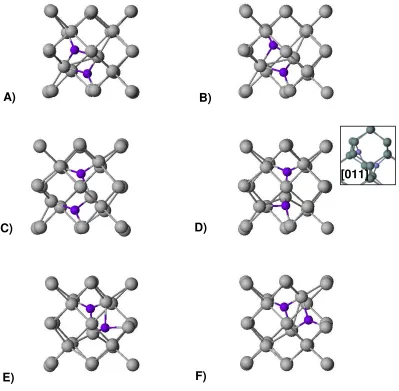
The different stages along the first diffusion path are illustrated in Figure 8. The two
nitrogen atoms part ways, one moving up while the other moves down, only to meet again on
the other side of the cell’s central atoms. The atoms move disjointedly, with the upper atom
moving through (2A-2C) before the lower atom does (2D-2F), while the highest energy
configurations are those where the nitrogen atoms are the farthest separated. In this [001]
projection, it appears that the configurations of Fig. 8D may be the pentagonal Humble
configuration (see Fig. 1), but from a different view (Fig. 8D inset) this is clearly not the
case. The nitrogen atoms maintain threefold coordination almost throughout the motion,
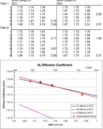
with the bond length varying from 1.44 to 2.33 , but mostly within 1.8±0.1 , see Table 1.
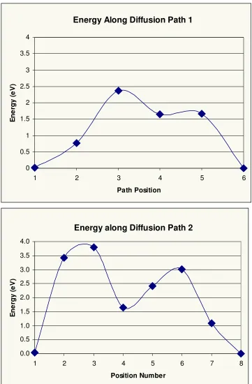
The activation energy for this diffusion series is only 2.37 eV (see Fig. 10A), considerably
less than any other published value, and ~0.4 eV below the experimental value mentioned
above. The diffusion coefficient prefactor, determined by calculating phonon frequencies for
the saddle point and the ground state, is 0.00377.
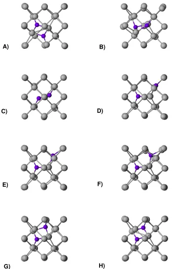
The second diffusion path is illustrated in Fig.9. In this series, the upper nitrogen
atom in Fig. 9A stays put while the other takes a round-about path towards the upper right
before rejoining its partner. Here, the highest energy configuration of Fig. 9B, (see Fig. 10B
for the relative total energy) happens when the two nitrogen atoms are closest together, in
contrast to the previous series. The mobile nitrogen atom then moves out and around to a
metastable low-energy configuration, see Fig. 9D, that once again resembles the Humble
model without actually assuming that configuration. An energy barrier of 3.8 eV separates
the original and metastable configurations, while a smaller barrier of 1.3 eV separates the
metastable stage from the final configuration. At the saddle point, one nitrogen atom is
four-fold coordinated while the other’s fourth nearest neighbor is only 2.71 away, see Table 1.
The metastable state (stage 4) in the path, on the other hand, has nitrogen bond lengths that
are quite similar to the lowest energy configuration. The interesting thing about this
diffusion path is that only one atom is required to be excited, as opposed to other models (the
previous model or those presented in [9]) that require both nitrogen atoms to pass through an
energy barrier. If thermal energy is plentiful in a material then it would not be unusual to
have two mobile atoms, whether they move disjointedly or in tandem. On the other hand,
result in a single atom doing all of the moving. This difference in likelihood is borne out by
a higher diffusion prefactor for the second diffusion path, with a value of 0.0248.
3.4 Discussion
The most significant way in which these diffusion paths differ from those previously
reported is that they are unconstrained with respect to the preservation of symmetric
arrangements, but instead follow non-obvious detours to maintain lower energy. It is not of
serious concern that the low value for the first diffusion mechanism does not match with the
experimental value, since error bars in this type of calculation can be as high as 0.4 eV.
Given that previous authors’ calculations have used the same inherent assumptions in their
models, the fact that this new path has a lower value must make it the preferred route.
Finally, nitrogen is known to introduce deep levels into the electronic band gap; this is the
reason that it does not work as a dopant in silicon.39 Due to the band gap problem in density
functional theory calculations, this introduces the potential for sizable error bars, despite
attempts to correct for it.38
3.5 Conclusion
Overall, we believe that, due to the energetics of the low activation energy diffusion
path presented here, this mechanism should be a strong contributor to the diffusion of
nitrogen, especially at elevated temperatures where the two atoms could move disjointedly in
a short time period without falling back from the saddle point into their original
configuration. The high activation energy diffusion pathway seems feasible and could be
required to move. A future study should explore these different paths competitively and at
different temperatures to get a closer idea of the dynamics and temperature dependence of
4 Anomalous Nitrogen Diffusion during Ion Milling: a SIMS Study
Submitted to Journal of Applied Physics as “Segregation and Enhanced Diffusion of
Nitrogen in Silicon Induced by Low Energy Ion Bombardment”, by N. Stoddard, G. Duscher,
A. Karoui, F. Stevie and G. Rozgonyi, February 2004
4.1 Introduction
Surface processes are ubiquitous in the semiconductor industry. Ion milling is used
for sample thinning, and etching, and in the creation of specialized structures.40,41 It is also a key part of the process to create thin foils for use in transmission electron microscopy.
Mechanical and chemical-mechanical polishing techniques are commonplace in any
semiconductor processing facility. One chief assumption in the use of these techniques is
that the resulting near-surface region is similar to the bulk material. For TEM specimens, the
hope is for the thin foil samples (almost always less than 100 nm thick, typically less than
10 nm thick) to have the same properties as the original bulk wafers. It has been established
that ion beam processes at moderate to high energy (> 5 keV) and incident angles greater
than 15º from the surface can cause significant damage in terms of point defect aggregates,
amorphization and even phase changes in the sample.42 In general, it is believed that using low energy, low angle conditions in ion milling minimizes the incidence of these defects. In
this paper, however, it will be shown that significant segregation effects occur in the N-Si
system during ion milling, even under optimum conditions, and that diffusion of N to a depth
of several microns is possible, despite the low energies involved. First, the different surface
processes will be described. The order of processes used here will correspond to the order
illustrated in Figure 12 involving mechanical polishing and dimpling, and subsequent ion
milling.
4.2 Materials and Methods
Two sets of samples were studied. The first set (Set A) represents the different stages
in TEM sample preparation: polishing, dimpling, and ion milling, carried out on
nitrogen-doped, Czochralski grown silicon wafers manufactured by Wacker-Nippon Silicon. They
have a bulk nitrogen concentration of 1*1015 atoms/cm3 and an oxygen concentration of
7*1017 atoms/cm3, as measured by SIMS. Of these, full thickness pieces were cleaved to ~1 cm on a side and measured in four states: 1) no processing (original 760 µm thickness), 2)
rough and fine mechanical polishing to 200 µm, 3) rough and fine dimple grinding to an end
thickness of 100 µm, and 4) ion milling in each of two ion mills: a Gatan 656 DuoMill and a
Fischione 1100 ion mill. It should be noted that the ion-milling was not intended to create a
hole, and the sample never came to a thin-foil state. For these bulk samples, ion
bombardment was from one side only. Separately, a 3 mm piece from the same wafer was
prepared as a TEM foil, see Fig. 13, using the various thinning processes described above.
Ion milling was done on both sides simultaneously in the Gatan mill. A hole was created and
a thin-foil region can be found around it. The SIMS measurement sites are numbered (1) –
(8). Note that an area of rough dimple grinding can be found containing craters (6) and (7),
where the sample broke during dimpling on a failed sample preparation sequence. A second
set, B, of Cz-Si samples comes from Agere Systems and has no grown-in nitrogen, but
or by thermal nitridation of the top 10 . The observed values for projected range and
straggle distance of the implant are 300 nm and 130 nm, respectively. According to theory,43 each N atom creates an average of 817 Frenkel Pairs, or 4.4*1022 FP/cm3. This is enough to
amorphize the 450 nm between the surface and Rp + ∆Rp. These samples had no heat
treatment and were ion-milled directly, on the top side only. Set B samples were ion milled
in the Fischione ion mill, and the nitrogen-implanted samples were ion milled with and
without liquid nitrogen cooling.
Polishing was performed using a Buehler Ecomet polisher with SiC pads whose grits
range from 400 to P4000. The final polishing step was a chemical/mechanical polish
involving a cloth pad and Syton NaOH colloidal fluid from MEMC. Dimple grinding was
done on a Gatan 656 Dimple Grinder using a brass wheel with 3 µm diamond paste and a
cloth wheel with 0.05 µm diamond paste. SIMS analysis was performed by the NCSU
Analytical Instrumentation Facility using a CAMECA IMS-6F Secondary Ion Mass
Spectrometer with a Cs+ primary beam and detection of negative secondary ions, primarily SiN-. Depth profiles were performed with the settings designed to attain the best detection
limit using a raster-reduction technique to improve nitrogen detection limit and differentiate
small signals from redeposition of sputtered material.44 A primary current of 400nA was used to sputter a region of 200 m x 200 m and secondary ions were detected from a 60 m
diameter region at the center of the raster. The raster was reduced to 90 m x 90 m and
4.3 Results
Table 2 provides the average nitrogen concentration for the first five to ten microns
for the different samples of set A. The bulk nitrogen concentration in the N-doped samples is
1*1015 cm-3; ion milled samples are measured to have 1016 cm-3, and the depth profiles for measurements on the TEM foil, see Fig. 14(a), were consistent with those on bulk samples,
see Figs. 15(a) and 15(b). Rough grinding, see Fig. 14(b), introduced the largest impurity
concentrations, which are probably particulate residue from the polishing compound.
Inspection of the sample using the scanning ion image during SIMS analysis revealed
particles of ~5 µm diameter whose carbon/nitrogen concentration was estimated to be on the
order of 1020 cm-3, in order to produce the average concentration of 5*1017 cm-3. Whatever the cause, the subsequent fine-polishing process, which occurs before ion milling, erases the
elevated concentrations and erodes the sample without any nitrogen accumulation. In fact,
the end concentration in the finely polished samples was actually slightly lower than the bulk
value. It should be noted that, in Figs. 14(b) and 14(c) the raster reduction technique was
used at ~9 µm and 1.7 µm depths, respectively. The silicon secondary ion yield increases at
those depths due to the collapse of the ion bombarded area to a smaller size. The nitrogen
level in Fig. 14(c) demonstrated a similar increase in raw data, but is calibrated, normalized
to the silicon increase, to show true concentration. Because it increases in step with the
silicon (so that the calibrated signal remains constant), the nitrogen signal cannot be due to
redeposited material and must originate from the sample. In Fig. 14(b), however, there is a
significant drop upon raster reduction, indicating that most of the signal at that depth is due
While the data on polishing is interesting, the key effect is the elevation of the
concentration due to ion milling. Craters (1) and (2) of the Gatan milled TEM foil had
concentrations of 1016 cm-3. On all ion-milled samples from Set A, as you move away from
the center of the ion-milled area, the concentration decreases smoothly towards baseline
values. The sharp rise at the end of the crater (2) profile, see Fig. 14(a), is due to
break-through, where a hole was actually created. Before break-break-through, however, there is a
significant rise in the concentration as the backside is approached. It should also be noted
that the concentration remains significantly elevated through several microns despite the
shallow (tens of angstroms) interaction depth of ion milling. The introduction of nitrogen
deep into the sample indicates an active mechanism for long-range diffusion. The thin foil
nature of the TEM sample apparently was not a significant factor, since the bulk ion milled
samples demonstrated similar behavior. Upon raster reduction, all of the samples in Set A
demonstrate an increase in secondary ion yield, indicating actual nitrogen in the sample. The
effect is not limited to a specific type of ion mill, since an older Gatan model with diffusion
pump and a newer Fischione model with a turbo-molecular pump had almost identical
results, see Figs. 15(a) and 15(b).
The data from the samples of Set B is shown in Figs. 15(c) and 15(d). Here, we see
that any drive-in by ion-milling through the ion-implanted region is minimal. This result was
independent of milling temperature and time in the ranges of –70 to 50ºC and one to three
hours. It should be noted that the raster-reduction method, when used on the ion milled
samples of Set B, did not show an increase in counts/second of SiN, indicating that the
nitrogen signal was not originating from the sample, but from redeposition from residual gas
samples in set A and approached the detection limit in the 1014 atoms/cm3 concentration range. The results for the nitride layer, see Fig. 16, were slightly different. While the
nitrogen level drops at 3 µm where the raster size is reduced, which indicates some signal
originating from redeposition, the signal is stronger than with the implanted sample. There
may be a mix of signal from redeposition with a small but real signal.
4.4 Discussion
The difference in behavior between the nitrogen-doped and nitrogen-implanted
samples can be explained. The nitrogen in the implanted samples is associated with a region
of ion implantation damage. Both amorphous silicon and dislocations will tend to trap the
nitrogen with high solubility, compared to the low solubility of defect-free crystalline silicon.
This trapping will prevent the nitrogen from being driven into the sample, allowing it to be
sputtered normally with the rest of the material. The lack of significant drive-in for the
nitrided sample can perhaps be attributed to the very shallow distribution, with only 10 of
nitride. The effective volume of cascades from the Argon ion milling is around 20 , so the
nitride may have been removed before the nitrogen could escape deeper in the sample. It is
conceivable that thicker surface concentrations might perform more favorably.
The explanation for the ion milling drive-in effect observed in the silicon whose
nitrogen was introduced during crystal growth requires one to consider the source of the extra
nitrogen observed. A few possibilities present themselves: i) that it is introduced from the
vacuum, ii) that there is a build-up of the nitrogen already in the sample, and iii) that it is
there would be a total of ~109 atoms/cm3 present in the ambient. If the nitrogen were being introduced by the ion milling, there is no reason why similar nitrogen-free silicon samples
would not experience the same nitrogen buildup: both the implanted silicon and the nitrided
silicon showed nothing of the sort once the top nitrogen-rich layers were removed.
Next, consider the mechanism of buildup from a ‘snow-plow’ effect of nitrogen in the
bulk of the sample. The behavior is determined by a combination of mass conservation and
segregation efficiency. Once again, the extremely optimistic case will be considered, where
the segregation coefficient is unity. Figures 14(a), 15(a) and 15(b) show an average
concentration of 8*1015 cm-3 over a depth of 8 µm. For the nitrogen to come from the sample
at a bulk concentration of 1*1015 to 2*1015 cm-3, a depth of 32-64 µm should have been ion
milled. In reality, at most 10 µm of material was ion milled, so this mechanism is not
sufficient to explain the results either.
The final possibility is that some surface contamination existed that was driven in by
the ion milling process. According to the above results, this contamination would have to be
significantly deeper than the 10 Å nitride layer that was examined. This mechanism is
difficult to quantify, but in the worst case, nitrogen-rich surface layers might be present with
~1*1022 atoms/cm3, or ~5*1014 atoms/cm2. In order to have enough material to drive in 1016 cm-3 of nitrogen through an 8 µm thick volume with a segregation coefficient of 0.01, a nitrogen-rich layer thickness of 8 nm would be needed. This thickness is at least reasonable,
both because it is not unrealistically thick and since it is considerably larger than the ion
milling interaction volume, which allows time to escape into the bulk (unlike the nitride
sample). Comparing Fig. 14(a) and Fig. 14(c), there is a surface peak before ion milling that
the largest amounts of material, but our attempts to verify it with surface nitrogen profiles
from implantation and thermal nitridation were unsuccessful. Support for the presence of
higher levels of nitrogen in the near-surface layers can be found in the reports of Karoui et
al., where SIMS N and O simultaneous depth profiling and imaging suggested that N and O
pile up at the subsurface during wafer polishing.45 They claim that, during polishing, the applied stresses from nano-scratches and dislocation micro-loops getter nitrogen which in
turn drag oxygen.
Independent of the mechanism of introduction, there is a second question as to how
the nitrogen moves through such a large depth. The thermal budget of nitrogen during ion
milling (<100ºC, 3h) is insignificant, so some type of enhanced diffusion is operating. One
possibility is the Crowdion mechanism of diffusion, where a series of atoms in a
close-packed direction slide together, pushing the last in the line into an interstitial position. Since
the N2 complex occupies a split-interstitial position, both direct Crowdion events and
increased interstitialcy would enhance diffusion. The Crowdion mechanism is particularly
active in ion-milling type processes, where collisions at the surface can create interstitials and
diffusion events deep in the sample. In general, the diffusion phenomenon seems to be
exotic and it is likely that other complementary mechanisms need to be examined.
4.5 Conclusion
Surveying the different surface techniques that have been considered, rough thinning
processes generally introduce highly impurity-rich embedded particles while subsequent fine
that CMP processes can still create extraordinary nitrogen concentrations within the first
micron. The ion milling process, however has been shown to induce significantly elevated
levels of nitrogen (up to 10X the bulk value) in the first several microns. It has been shown
above that this magnitude of change to a TEM sample can significantly affect TEM analysis.
There should also be some impact on devices created in nitrogen-doped silicon that involve
reactive ion etching, although that has yet to be studied. Two significant phenomena have
been observed, however. First, a segregation mechanism is operating to accumulate the bulk
nitrogen and to incorporate nitrogen driven in from the first few nanometers of the surface.
Second, an unusual diffusion mechanism is causing the segregated nitrogen to diffuse
through several microns of the sample despite a small thermal budget. The Crowdion
mechanism has been suggested to explain the nitrogen diffusion, but more investigation is
5 The Nucleation and Growth of Extended Defects in Silicon from their atomic constituents
Submitted to Physical Review B as “Inducing the Nucleation and Growth of Extended
Defects at Room Temperature in Silicon by 200kV Electron Irradiation” by N. Stoddard, G.
Duscher, W. Windl and G. Rozgonyi, June 2004.
5.1 Materials and Methods
[100] oriented, as-grown N-FZ and N-CZ plan-view samples were prepared by
conventional TEM thinning methods, which include grinding, polishing, dimple grinding and
ion milling. Siltronic Corp. grew the N-CZ starting material while the N-FZ sample came
from the National Renewable Energy Labs. The N-CZ sample has bulk light element
impurity profiles of [O] = 7*1017 cm-3 and [N] = 1015 cm-3 while the N-FZ sample has [O] = 1015 cm-3 and [N] = 1015 cm-3. Samples from these wafers were prepared for TEM analysis
by mechanical polishing, dimple grinding and ion milling with 3-5 keV Ar+ ions at 5-6 mA. It has already been shown that this type of sample preparation can result in enhanced bulk
nitrogen concentrations of up to 1016 cm-3. Separately, a piece of the sample of the as-grown N-CZ Si was annealed using a hi-lo cycle of 8 hours at 750ºC and 16 hours at 1050ºC. It was
prepared as a cross-sectional TEM sample and [110] oriented for irradiation. All electron
irradiation was performed at 200 kV in JEOL 2010F and Topcon 002B electron microscopes,
while high-resolution imaging, EELS, and scanning TEM (STEM) in Z-Contrast and bright
field modes were performed on the JEOL instrument. It should be noted that contamination
every time they are placed in the microscope, and Z-contrast analysis is typically done at a
different time than the irradiation.
Simulations were performed using the Vienna Ab Initio Simulations Package
(VASP), which employs a self-consistent approach based on density functional theory in the
local density approximation. Ultra-soft pseudopotentials with a plane-wave basis set were
used both for ionic relaxation and for calculating the total energy at different points along the
diffusion path. A perfect supercell of 64 silicon and two nitrogen atoms, i.e. eight unit cells,
was first relaxed with the well-known N2 structure consisting of two nitrogen and two silicon
atoms in a square configuration in the [110] direction. A similar configuration with the
nearest silicon atom to the N2 pair situated in a near-by interstitial position was relaxed, and
four to six intermediate positions between these two were interpolated as starting guesses for
nudged elastic band calculations. Each of the intermediate steps was then locally relaxed
along its hypertangent to a total energy tolerance of 0.005 eV. Only the neutrally charged
case is considered, since in other work the energy difference between negative and neutral
charge states was negligible while the positive charge state had higher energies by a constant
energy shift.18
5.2 Results
Figure 17 depicts a N-CZ Si sample in both bright field and Z-Contrast modes of the
STEM. The dark and light arcs visible in A) and B), respectively, delineate the boundary of
the irradiated region. The irradiation was positioned near the edge of the TEM foil for best
results in Z-Contrast and EELS modes of the TEM. In Z-Contrast images B), C) and D), the
bright areas are denser (i.e. interstitial rich) or thicker, as was the case in Fig. 4. As was
noted earlier, Z-Contrast image features are generally due to differing elemental distributions
(based on atomic number Z), varying sample thickness or density fluctuations.36 Since this
sample is pure CZ silicon (the nitrogen influence is negligible), we can attribute the contrast
to local Si density variations due either to vacancies or silicon self-interstitials, local
thickness differences or the presence of extra layers of oxide. It should be noted that silicon
dioxide is very close in mass density to normal silicon, but since RBS goes as Z2, an oxide layer will give less signal than an equal thickness of silicon. If, on the other hand, extra
oxide thickness is on top of an equal thickness of silicon, the signal will be additive and give
higher contrast to this region. Previously, secondary phases were observed but not identified.
Here, as in Figs. 17C and 17D, EELS chemical analysis shows that high oxygen
concentrations exist both inside the large irradiated region and in a speckled ring just outside
of it. It is logical that the elastic collisions resulting from TEM electron bombardment will
greatly enhance oxygen diffusion in the same way that silicon interstitial diffusion is
enhanced. For oxygen diffusing in a vacancy-rich environment, the eventual result will be
clustering and precipitation. Ripening of oxygen clusters inside the irradiated zone has been
observed as longer irradiation times are used, a process that competes with diffusion out of
the beam volume. While nitrogen concentrations were too small for measurement by EELS,
the oxygen is readily detected and has some dramatic effects. Consider, for example, the two
large bright spots in Figs. 17C and 17D. The sharply defined EELS spectra, see Fig. 17E, for
the boxed area in Fig. 17C clearly indicates the presence of pure silicon dioxide, based on the
interstitial oxygen. The Fig. 17C particle has fairly distinct boundaries, while the bright area
in 17D has softer edges and is a mix of silicon with interstitial oxygen and silicon dioxide, as
indicated by its EELS spectrum. No particle like either of these two was found elsewhere in
the sample, i.e. outside of the irradiated zone, and they were not present before irradiation.
As such, they must be attributed to e-beam-induced clustering and precipitation.
In nitrogen-doped, low oxygen float zone silicon, there exist differences in the
response to irradiation, compared to the CZ material. Instead of the aggregation of oxygen,
we observed void formation due to the agglomeration of vacancies during irradiation.
Evidence of this phenomenon can be found in Figure 18. First, it should be noted that the
three bright spots in Fig. 18B are due to carbon contamination while the converged Z contrast
e-beam rested in spot-mode at those positions. Even though carbon has a lower Z than
silicon, these spots appear bright because of the thickness of the carbon added on top of the
sample thickness. The sample material in Fig. 18 is N-FZ Si, and the concentration of
oxygen is a factor of 1000 less than in the N-CZ material. For this reason, oxygen
precipitation is not expected, and no evidence of clusters can be seen in Fig. 18B. Instead,
closer examination of the irradiated area in Z contrast mode reveals small dark features, see
Fig. 18C. By the same logic as is used above, these can only be aggregates of vacancies.
Their triangular appearance when viewed in high resolution suggests that the voids are
somewhat faceted and vary in size from 2-5 nm, see Fig. 18D. Evidently, nitrogen-doped FZ
silicon exhibits the same separation of interstitials and vacancies described above for N-CZ
samples, but without the oxygen clustering. The irradiated area appears in Fig. 18B as a dark
circle whose weaker contrast corresponds to a lower concentration of silicon atoms, i.e. a
aggregate into voids. A diffuse brighter halo of excess interstitials surrounds the dark circle,
as was the case for N-CZ Si. In addition to the halo, faint bright lines can be seen directed
radially away from the ring, and corresponding to the open (110) directions. The implication
of this result is that the interstitial diffusion can continue outside of the irradiated region in
certain directions. This is not necessarily surprising since the sample is maintained in the
TEM at a temperature below 350K, while diffusion of silicon self-interstitials has been
reported below 100K.5 It is also a reinforcement of the bulk nature of the diffusion, since channeling along (110) directions is a significantly weaker phenomenon in surface diffusion.
The results of different intensities of irradiation are found in Figure 19. In 19A, a
hole has been created by intense convergent beam irradiation of the N-CZ Si thin foil. This
type of hole formation by electron irradiation has been widely observed in thin film silicon
samples, and is generally attributed to surface diffusion.46 The interesting result here is that a stacking fault has nucleated in close proximity to the hole, presumably formed from atoms
diffusing in the bulk by interstitial paths away from the beam. With a beam of ~60 nm
diameter, as in Fig. 19B, amorphization of the silicon crystal occurs but a hole is never
formed. The amorphous nature of the irradiated region is verified by convergent beam
electron diffraction patterns (inset), where the crystalline diffraction contrast is mostly lost in
the irradiated area.
Finally, the electron knock-on process in nitrogen-doped silicon was studied using a
nudged elastic band calculation. The configurations along the path of the knock-on event are
shown in Figure 20, while the energetics can be found in Fig. 21. The initial configuration is
site, see Fig. 20-11. There are two saddle points along this path: at 4.2 eV above the ground
state in Fig. 20-5 and at 6.2 eV above the ground state, found in Fig. 20-10. Two of the
configurations (6 and 9 in Fig. 21) are omitted because they provide no interesting
information. The excited atom, highlighted in yellow, moves away from the N2 pair.
Meanwhile, a nearby atom is drawn in to re-form a [110]-oriented N2 square, see the white
star in Figs. 20-3 to 20-5. Configuration 20-5 is a local saddle point, proceeding to a local
minimum in 20-8. In the series from 20-5 to 20-11, the atom indicated by the black star is
kicked out to accommodate the excited atom, and in Fig. 20-8, the system is very close to
reverting to the original configuration with three atoms exchanged. If the excited atom
(highlighted) does not have the energy to move through the saddle point of Fig. 20-10, there
would be no observable change and no net damage. In the case that the excited atom moves
to the final configuration, the atom indicated by the black star determines where the vacancy
ends up; the lower energy configuration, shown in 20-11 is for a VN2 complex to form. This
is the first configuration that is stable against reversion to something equivalent to Fig. 20-1,
with a 1 eV energy drop from 20-10 to 20-11. The total formation energy for the final
configuration is 5.3 eV. To evolve the system one step beyond 20-11, a similar calculation
was carried out to find the energy barrier between this interstitial position and the next
interstitial position, one step farther from the N2 pair. To get the excited atom farther away, a
supercell of twice the size, 128 atoms, was used with 64 atoms of pure Si added. The
energies of the initial and final interstitial states are within 0.2 eV, with an intermediate
saddle point at 1 eV higher energy than 20-11. This value for the migration barrier energy is
5.3 Discussion
The surface is a consideration that must be taken into every interaction in a thin foil.
In this case, it might be tempting to explain the effects noted in Figs. 4, 17 and 18 as surface
related. The argument would be that only the atoms on the surface are being manipulated to
move outside of the beam, and that the resulting thickness variation causes the ring-shaped
contrast. In the case of the oxide formation in Fig. 17, one might surmise that the silicon
dioxide particles have simply coalesced from the native surface oxide. For Fig. 18, the dark
spots could be faceted [111] surface pits, once again the result of surface manipulation.
There are several problems with these arguments, however. First of all, there is the question
of reference samples. It was previously mentioned that nitrogen-free samples have
essentially no response to irradiation with beams larger than 20 nm in diameter. In some
N-free samples, slight stress contours were discernible after irradiation, but in most even this
was lacking, and in no N-free sample were there features like those in the Z contrast
micrographs. In the study by Yamasaki and Takeda[31], damage could only be created in Si
under 200kV irradiation by cooling the sample down to 15K. The only difference between
the N-free reference samples (similar to those used in [31]) and the N-doped samples was the
bulk nitrogen concentration, so that the fundamental interaction during irradiation is
indicated to occur at the bulk nitrogen sites. Secondary Ion Mass (SIMS) depth profiles have
demonstrated that the nitrogen concentration after TEM sample preparation is uniformly
distributed at a level of ~1016 cm-3. Concerning the arguments about thickness differences, attempts have been made to profile the topography of the irradiated surface using atomic
surface oxide has some response to irradiation. In fact, irradiation under a tightly converged
beam often causes oblation of the surface oxide. In Fig. 17D, however, the energy-loss
spectrum of Fig. 17E tells us that interstitial oxygen is piled up here, and this interstitial
oxygen would have had to move by bulk diffusion. A similar situation is found in Fig. 19,
where stacking faults have nucleated near a hole that was created during irradiation by a
2-3 nm converged electron beam. Holes like this are readily observed as a result of
converged-beam irradiation in silicon thin foils, and it is often assumed to be an artifact related to
surface diffusion. In this case, however, it is not possible for the stacking fault to have been
nucleated by atoms diffusing along the surface because there is no driving force outside of
the beam to force surface atoms into the bulk. Instead, atoms kicked out of their lattice sites
have diffused in the bulk via interstitial pathways, and aligned themselves so as to lower the
local energy. While some surface diffusion cannot be ruled out, it is likely that the two
mechanisms compete during irradiation. In the case of Fig. 19B, however, there is no way
for amorphization of the sample to occur through surface rearrangement. This result can
only be explained by a bulk interaction at a high rate of damage accumulation. In N-free Si,
amorphization was never achieved with a 200kV beam, even at 15K and with electron doses
of 1023 cm-2, but the nitrogen interaction proves here to be strong enough to facilitate breakdown of the crystal structure through repeated interaction with the silicon point defects.
It was noted earlier that the hole creation process in Fig. 19 does not involve nitrogen
in the creation of vacancies that eventually grow to be a hole. It was determined that, based
on Rutherford scattering, a 200kV electron can impart up to 18 eV of energy to a silicon
atom, see above. First principles calculations indicate that the knock-on energy to create a
end of this energy range tend to quickly recombine in molecular dynamics simulations of the
final configuration at room temperature. It is likely that this knock-out/recombination
process occurs regularly during routine TEM analysis. Consider that, under typical
conditions of the Topcon 002B TEM beam exposure (i.e. 10 µA, 400 nm beam diameter),
~3.1*105 electrons will flow through an area of 0.0625 nm2 every second.* Based on the graph presented in Fig. 3, the probability for each individual electron to impart more than 15
eV to one silicon atom is P 0.0000025.† Calculating the probability for interaction in one second as one minus the probability that none of the electrons will interact,
( )
1s =1−(
1−P( )
1e−)
310,000 =1−0.9999975310,000 ≈0.54 Pthe result is close to a coin toss. Using the same expression, the probability of an electron
imparting the maximum possible energy (18.6 eV) to one of the atoms in a 100 nm thick
column in 1s is 0.79! Our conjecture is that permanent separation requires a second electron
collision to occur before the Frenkel pair recombines (in the absence of nitrogen). According
to simulations, recombination of the V-I pair within 100 ps is quite likely. However, in
either the Topcon 002B or the JEOL 2010F microscope with a beam diameter of 100-400
nm, the probability of any electron passing by a particular place in a period of 100 ps is
3.1*105 e-/s *10-12 s 0.00001, and much less that an electron that will impart significant
energy to the displaced atom. Under these broad-beam irradiation conditions, recombination
should dominate. Hole creation is usually observed at a beam diameter of <5 nm, where the
picture changes dramatically. In the JEOL 2010F, with 1 µA of beam current flowing
through an area ~2 nm in diameter, there will be ~12 electrons passing through each
0.0625 nm2 every 100 ps, so that a second low energy collision to further separate the Frenkel pair before recombination becomes a real possibility. The repetition of this process
over several tens of seconds results in the observed rapid out-diffusion of silicon atoms from
the irradiated volume via bulk and surface diffusion.
The results of the nudged elastic band calculation add an interesting follow-on to the
discussion of knock-on processes. It appears that the N2 defect causes the barrier to Frenkel
pair creation to be lowered from the reported range, 11-20 eV, to a value around 6 eV. For
argument, let us take a moderate value for the displacement energy of Ed = 15 eV. In Fig. 3,
the nitrogen-enabled knock-on energy has a higher probability, P = 0.00015, than the 15 eV
event with P = 0.00001 by a factor of 15. In the course of 1s irradiation, the probability of a
nitrogen-enabled V-I separation at any particular N2 site is near unity, but the probability of
an event in pure silicon is still 0.54 for every atom, and there ~106 as many bulk silicon atoms as there are silicon atoms near an N2 pair, so the pure silicon interaction should still be
more prevalent. Therefore the calculated lowering of the energy barrier to Frenkel pair
formation is not sufficient to account for the dramatic difference in response to irradiation
between nitrogen-doped and nitrogen-free samples. Two alternative arguments can be made.
First, one could argue that the effective value of Ed, accounting for a temperature dependence
of the spontaneous recombination volume, is actually above 18.6 eV at room temperature.
This properly explains the damage observed at 15K under electron irradiation, but is not
entirely satisfying since the process of hole formation as explained above makes it clear that
even the fastest recombination events can be disrupted given the right conditions. Instead, to
properly account for the observational differences, one must look to the stability of the