Analysis Parameter of 2-D Discrete Wavelet
Transform using Multiplier-less Technique
Neha Jain, Prof. Ansul Awasthi, Dr. Manish Gurjar
M. Tech. Scholar, Dept. of Electronics and Communication, Technocrats Institute of Technology, Bhopal, India Assistant Professor, Dept. of Electronics and Communication, Technocrats Institute of Technology, Bhopal, India
HOD, Dept. of Electronics and Communication, Technocrats Institute of Technology, Bhopal, India
ABSTRACT: Conventional distributed arithmetic (DA) is popular in field programmable gate array (FPGA) design, and it features on-chip ROM to achieve high speed and regularity. In this paper, we describe high speed area efficient 2-D discrete wavelet transform (DWT) using 9/7 filter based new efficient distributed arithmetic (NEDA) Technique. Being area efficient architecture free of ROM, multiplication, and subtraction, NEDA can also expose the redundancy existing in the adder array consisting of entries of 0 and 1. This architecture supports any size of image pixel value and any level of decomposition. The parallel structure has 100% hardware utilization efficiency.
KEYWORDS: 2-D Discrete Wavelet Transform (DWT), NEDA, Low Pass Filter, High Pass Filter, Xilinx Simulation. I. INTRODUCTION
Discrete wavelet transform (DWT) is a mathematical technique that provides a new method for signal processing and decomposes a discrete signal in the time domain by using dilated / contracted and translated versions of a single basis function, named as prototype wavelet [Mallat (1989a) ; Mallat (1989b) ; Daubachies (1992) ; Meyer (1993) ; Vetterli and Kovacevic (1995)]. DWT offers wide variety of useful features over other unitary transforms like discrete Fourier transforms (DFT), discrete cosine transform (DCT) and discrete sine transform (DST). Some of these features are; adaptive time-frequency windows, lower aliasing distortion for signal processing applications, efficient computational complexity and inherent scalability [Grzesczak et al. (1996)]. Due to these features one dimensional (1-D) DWT and two dimensional (2-D) DWT are applied in various application such as numerical analysis [Beylkin et al. (1992)], signal analysis [Akanshu and Haddad (1992)], image coding [Sodagar et al. (1999); Taubman (2000)], pattern recognition [Kronland et al. (1987)], statistics [Stoksik et al. (1994)] and biomedicine [Senhadji et al. (1994)]. Several algorithms and computation schemes have been suggested during last three decades for efficient hardware implementation of 1-D DWT and 2-D DWT.
implemented in a VLSI system to meet the temporal requirement of real-time application. Keeping this fact in view, several design schemes have been suggested in the last two decades for efficient implementation of 2-D DWT in a VLSI system. Researchers have adopted different algorithm formulation, mapping scheme, and architectural design methods to reduce the computational time, arithmetic complexity or memory complexity of 2-D DWT structures. However, the area-delay performance of the existing structures changes marginally. This is mainly due to the memory complexity, which forms a major hardware component of folded 2-D DWT structure. A detail study of the existing design methods and a complexity analysis is made in Chapter 2 to find an appropriate design strategy to improve the area-delay performance of 2-D DWT structures.
II. MULTILEVEL DISCRETE WAVELET TRANSFORM
Multiresolution analysis (MRA) is a characteristic feature of SB and it is used for better spectral representation of the signal. In MRA, the signal is decomposed for more than one DWT level known as multilevel DWT. It means the low-pass output of first DWT level is further decomposed in a similar manner in order to get the second level of DWT decomposition and the process is repeated for higher DWT levels. Few algorithms have been suggested for computation of multilevel DWT. One of the most important algorithm are pyramid algorithm (PA), this algorithm are proposed Mallet (1989a) for parallel computation of multilevel DWT. PA for 1-D DWT is given by
)
2
(
)
(
)
(
11 0
i
n
Y
i
h
n
Y
ljk
i j
l
(1))
2
(
)
(
)
(
11 0
i
n
Y
i
g
n
Y
hjk
i j
h
(2)Where
Y
j(
n
)
l is the n-th low-pass sub band component of the j-th DWT level and
Y
(
n
)
jh is the n-th high-pass sub
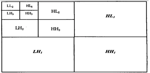
band component of the j-th DWT level. Two-dimensional signal, such as images, are analyzed using the 2-D DWT. Currently 2-D DWT is applied in many image processing applications such as image compression and reconstruction [Lewis and Knowles (1992)], pattern recognition [Kronland et al. (1987)], biomedicine [Senhadji et al. (1994)] and computer graphics [Meyer (1993)]. The 2-D DWT is a mathematical technique that decomposes an input image in the multiresolution frequency space. The 2-D DWT decomposes an input image into four sub bands known as low-low (LL), low-high (LH), high-low (HL) and high-high (HH) sub band.
III. PROPOSEDARCHITECTURE
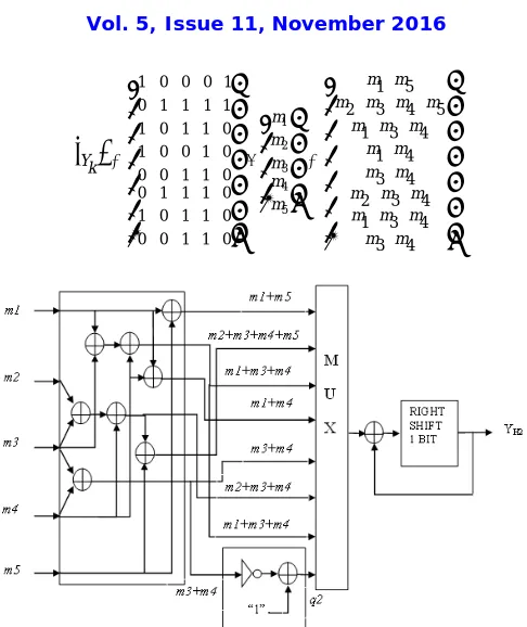
The block diagram of 9/7 wavelet coefficient based multilevel discrete wavelet transform using NEDA structure shown in figure 2. In this figure, input sample passing through 8-bit register after that all symmetrical delay input is add in the equation 3 to equation 7.
) 6 ( ) ( ) 1
( X n X n
r
r(2)X(n1)X(n5) r(3) X(n2) X(n4
)
r(4)X(n3)We have used NEDA in 9/7 filter to remove multipliers. We have to apply NEDA two times get the 1-D 9/7 filter high pass output
Y
H1and low pass outputY
L1 . Whereh
0 ,h
1 ,h
2 ,h
3 ,h
4 are the Low pass filter coefficients andg
0,g
1,g
2,g
3are the High pass filter coefficients.If we take the high pass coefficients
g
0,g
1,g
2andg
3 applied NEDA technique byr
1,r
2,r
3andr
4then we get the high pass outputY
H of the 9/7 filter and we take the low pass coefficienth
0,h
1,h
2,h
3, andh
4applied NEDAtechnique by
m
1,m
2,m
3,m
4andm
5 then we get the low pass outputY
Lof the 9/7 filter. Example the low passoutput step by step as shown in below:
5 4 3 2 1 4 3 2 1 0 m m m m m h h h h h L YLet
m
1
1
,m
2
2
,m
3
3
,m
4
4
andm
5
5
. Then multiplier row and column and find out the low pass output 122. Whereh
0,h
1,h
2,h
3, andh
4daubechies 9/7 filter coefficients are 0.6029490, 0.2668444, 0.782232, -0.0168641 and 0.02674875 respectively. All the daubechies 9/7 filter coefficients multiplied by 128 and get the 77, 34, -10, -2 and 3 respectively. 122
5 4 3 2 1 3 2 10 34
77
H YWe take the low pass coefficients
h
0,h
1,h
2,h
3, andh
4applied NEDA technique bym
1,m
2,m
3,m
4andm
5 then we get the low pass outputY
Lof the 9/7 filter.
5 4 3 2 1 00000011 11111110 11110110 00100010 1001101 0 m m m m m L YNow we can make the DA matrix by the filter coefficients as low pass filter based DA matrix
4 3 4 3 1 4 3 2 4 3 4 1 4 3 1 5 4 3 2 5 1 0 0 0 1 1 1 1 1 1 0 0 1 0 1 0 0 1 1 0 0 0 1 0 0 1 0 1 1 0 1 1 1 1 1 0 1 0 0 0 1 5 4 3 2 1 m m m m m m m m m m m m m m m m m m m m m m m m m m k YIN Figure 2, apply NEDA techniques step-1 all the input converts’ binary number
001
1
m
,m
2
010
,m
3
011
,m
4
100
,m
5
101
Step-2 all the binary input applied to sign extension so,
0001
)
1
(
s
,s
(
2
)
0010
,s
(
3
)
0011
,s
(
4
)
0100
,s
(
5
)
0101
Step-3 all the sign extension input applied to adder array so,0110
)
1
(
m
,m
(
2
)
1110
,m
(
3
)
1000
,0101
)
4
(
m
,m
(
5
)
0111
,1001
)
6
(
m
,m
(
7
)
1000
1001
1
)
(
)
8
(
not
m
3
m
4
m
Step-4 the entire adder array input applied to MUX so, The entire adder array input
m
(
1
)
right shift 1-bit so MUX (1) = 0’0110 =Yp (0)MUX (1) add MUX (2) = YP (1)
= 0’0110 = 1110 + 100010
Output of the YP (1) again right shift 1-bit and adds MUX (3) so
= 0’100010 = 1 000 + 1 100010
Continuous the process one by one, after then calculate the final output YP (7) = 00001111010 = 122
Carry is rejected.
For 2-D sub-band WT, the outputs of 1-D high pass and low pass filters
Y
H1andY
L1are passed through series of shift registers and then we take the samples parallel using parallel data access method. The parallel data access method is used to minimize the memory requirement in 2-D sub-band WT.IV. SIMULATION RESULT
All the designing and experiment regarding algorithm that we have mentioned in this paper is being developed on Xilinx 6.2i updated version. Xilinx 6.2i has couple of the striking features such as low memory requirement, fast debugging, and low cost. The latest release of ISETM (Integrated Software Environment) design tool provides the low memory requirement approximate 27 percentage low. ISE 6.2i that provides advanced tools like smart compile technology with better usage of their computing hardware provides faster timing closure and higher quality of results for a better time to designing solution. By the aid of that software we debug the program easily. Also included is the newest release of the chip scope Pro Serial IO Tool kit, providing simplified debugging of high-speed serial IO designs for Virtex-2 FX and Virtex-E LXT and SXT FPGAs. With the help of this tool we can develop in the area of communication as well as in the area of signal processing and VLSI low power designing.
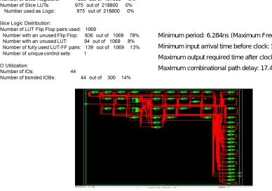
We functionally 2-D sub-band WT verified presented in this paper including all low pass filter and high pass filter. We have been found from the results shown in table 1, that number of slices, number of slices LUTs and maximum combinational path delay used in different types of device family. RTL (resister transistor logic) view is 2-D sub-band tree structure in shown in figure 3.
Table 2: Second Level DWT
Table 3: Comparison result of existing algorithm and proposed algorithm
Design Number of Slice LUT Slice Registers Minimum Period Total Memory Usage
Linning Ye - 159 1.78 nsec 447
- 384 12.9 nsec 204.7
Proposed Design 206 37 1.155 nsec 316
975 233 6.284 nsec 240
Figure 3: RTL View of Second Level Wavelet Transform
Minimum period: 6.284ns (Maximum Frequency: 159.132MHz) Minimum input arrival time before clock: 5.945ns
V. CONCLUSION
2-D sub-band wavelet transform standardize two basic blocks for representing the image compression namely, low pass filter and high pass filter. Wavelet transforms a vast application in many areas like image compression, signal processing and VLSI design. We propose a 2-D sub-band novel distributed arithmetic paradigm named NEDA structure for VLSI implementation of digital signal processing (DSP) algorithms involving inner product of vectors and vector-matrix multiplication. We demonstrate that NEDA is a very efficient architecture with adders as the main component and free of ROM (free memory), multiplication, and subtraction. For the adder array, a systematic approach is introduced to remove the potential redundancy so that minimum additions are necessary.
REFERENCES
[1] S.G. Mallat, “A Theory for Multiresolution Signal Decomposition: The Wavelet Representation”, IEEE Trans. on Pattern Analysis on Machine Intelligence, 110. July1989, pp. 674-693.
[2] M. Alam, C. A. Rahman, and G. Jullian, ”Efficient distributed arithmetic based DWT architectures for multimedia applications,” in Proc. IEEEWorkshop on SoC for real-time applications, pp. 333 336, 2003.
[3] X. Cao, Q. Xie, C. Peng, Q. Wang and D. Yu, ”An efficient VLSI implementation of distributed architecture for DWT,” in Proc. IEEEWorkshop on Multimedia and Signal Process., pp. 364-367, 2006.
[4] Archana Chidanandan and Magdy Bayoumi, “AREA-EFFICIENT NEDA ARCHITECTURE FOR THE 1-D DCT/IDCT,” ICASSP 2006.
[5] M. Martina, and G. Masera, ”Low-complexity, efficient 9/7 wavelet filters VLSI implementation,” IEEE Trans. on Circuits and Syst. II, ExpressBrief vol. 53, no. 11, pp. 1289-1293, Nov. 2006.
[6] M. Martina, and G. Masera, ”Multiplierless, folded 9/7-5/3 wavelet VLSI architecture,” IEEE Trans. on Circuits andsyst. II, Express Brief vol. 54, no. 9, pp. 770-774, Sep. 2007.
[7] Gaurav Tewari, Santu Sardar, K. A. Babu, ” High-Speed & Memory Efficient 2-D DWT on Xilinx Spartan3A DSP using scalable Polyphase Structure with DA for JPEG2000 Standard,” 978-1-4244-8679-3/11/$26.00 ©2011 IEEE.
[8] B. K. Mohanty and P. K. Meher, “Memory Efficient Modular VLSI Architecture for High throughput and Low-Latency Implementation of Multilevel Lifting 2-D DWT”, IEEE TRANSACTIONS ON SIGNAL PROCESSING, VOL. 59, NO. 5, MAY 2011.
[9] B. K. Mohanty and P. K. Meher, “Memory-Efficient High-Speed Convolution-based Generic Structure for Multilevel 2-D DWT”, IEEE TRANSACTIONS ON CIRCUITS SYSTEMS FOR VIDEO TECHNOLOGY.