Volume 8, No. 3, March – April 2017
International Journal of Advanced Research in Computer Science RESEARCH PAPER
Available Online at www.ijarcs.info
Expanding the UVM Register Model towards Automation and Simplicity of Use
Abhishek Jain ECE Department
Jaypee Institute of Information Technology Noida-201309, India
Richa Gupta ECE Department
Jaypee Institute of Information Technology Noida-201309, India
Abstract: The standard UVM register package contains built-in test sequences library which is used to perform most of the basic register and memory tests. These sequences are very useful at IP level verification but at SoC level verification, these sequences take very long time to run. Similarly, currently users require strong knowledge of SystemVerilog UVM language to use UVM_REG model. Some limitations in current UVM_REG package like no automatic data checking for memory accesses and limited support for memory burst operation were also seen. In this paper, we are describing how we addressed the above mentioned issues. We are accessing processor programmable registers and memories through a standard UVM_REG API. This API is aimed at writing simpler directed tests which require less or no SystemVerilog/UVM understanding. This API can be used to facilitate dumping register access for reuse from IP to SoC, or format outputs for use in ATE test vectors development etc. We also developed our own register/memory sequences to address the SoC level register and memory testing. Customized code is written to enhance the features of standard UVM_REG model. IP-XACT based tools are also developed to automatically generate all required verification environment files for using standard register model.
Keywords: IP-XACT; Register Model; Register Sequences; SystemVerilog; Universal Verification Methodology (UVM); UVM_REG
I. INTRODUCTION
Universal Verification Methodology (UVM) is the first standard, interoperable, open, and proven verification re-use methodology. UVM is used for the functional verification of digital hardware, mainly using simulation. A SystemVerilog UVM test bench consists of reusable verification components. A verification component is a configurable, encapsulated, ready to use, verification environment for a design sub-module, an interface protocol, or a full system [1, 2]. Each verification component follows a standard architecture for stimulus generation, data/protocol checking, and obtaining coverage information for a specific design or protocol. The verification environment is applied to the designs to verify implementation of the protocol or design architecture [3]. UVM based UVM_REG register model is mainly used to make it easier to write reusable register/memory sequences that access hardware registers and memory areas. The register model data structure is designed to show an image of the Design Under Test (DUT) hierarchy and this makes it easier to write reusable and abstract stimulus in terms of hardware blocks, registers and fields, memories rather than working at a lower bit pattern level of abstraction. The register model contains a number of read/write access methods which sequences use to read and write registers. These methods results in conversion of generic register transactions into the target bus transactions [3, 4].
The UVM register package contains built-in test sequences library which is used to perform most of the basic register and memory tests, such as testing of register reset values and testing of the register and memory data paths. Using register attributes, these tests can be disabled for those locations of the register or memory map where they are not relevant.
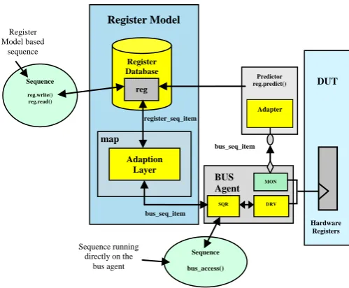
Fig. 1 represents a verification environment with UVM registers integrated [3, 12]. As a verification environment gradually develops, verification users need to develop analysis components such as scoreboards and functional coverage monitors which refer to the content of the register
model in order to check behavior of the DUT or to make sure that it has been tested in all required configurations.
Figure 1. Verification Environment with UVM Registers Integrated
In our verification environment, UVM_REG register and memory model is used for efficient verification of register and memory. This is used in conjunction with the register/control bus interface UVC, so that whenever the IP/SoC registers are read/written, the associated UVM_REG register and memory model pre-defined registers are also updated and IP/SoC register contents are verified by a self-checking mechanism [5, 6]. UVM_REG built-in test sequences are very useful at IP level verification but at SoC level verification where number of registers are very large, these sequences take very long time to run and testing the internal of the IP at SoC is not that relevant. Thus, we developed additional register and memory sequences to address SoC level register and memory verification needs.
Predictor
reg.predict() DUT
Hardware Registers Register
Database Sequence
reg.write() reg.read()
reg
Adaption Layer
Sequence
bus_access()
Register Model Register
Model based sequence
Sequence running directly on the
bus agent
Adapter
BUS Agent
register_seq_item
bus_seq_item
map
SQR bus_seq_item
MON
This paper is organized in paragraphs presenting the flow we’ve developed going through an architectural representation of the register model, including memories, and what can be done to facilitate, and complete the register testing on the Design Under Test. Functional tests run on a host processor often program address mapped registers and memories. Therefore the flow covers the use of the register model into functional tests.
Register Model Golden Specification
Register Model Golden Specification
(machine readable)
Uvm_reg based
model Test sequences
Functional Test API
Register testing
Ready for use in functional
tests
√
Specification
Automated Register
model generation &
test collaterals
Figure 2. Developed Flow of Register and Functional Tests
In Fig. 2, first is explained how to go from the architecture register model golden specification to a machine readable specification and the choices being made there. Then the expansion and automation to the uvm_reg register model is shown, including memories handling, and bus considerations. Test sequences are explained, as well as examples of a functional test API simplifying the use by non UVM experts.
The end result is a flow that provides 100% of the register testing capability and is a code library that facilitates the development of functional tests. While we would like to compare our specific register APIs against APIs developed by others, it is not possible since there are no publicly available register APIs for us to compare against. This journal paper is extended version of the conference paper (28th International Conference on VLSI DESIGN, January 2015, Bangalore) [3].
The following Section discusses the new register and memory sequences which are mainly used for register and memory level verification (not for functional verification).
II. RELATED WORK
K. A. Meade and S. Rosenberg covered the concepts and goal from which the design and implementation of the UVM was derived [1]. They also shared problems of verification engineers and their proven solutions that were expected to be added to the SystemVerilog UVM library in the future.
Sharon Rosenberg provided useful information to verification engineers to either verify their current register verification methodology or follow the right steps to move to the UVM_REG register model. He also provided several
code examples to implement the recommendations easily. Tudor Timisescu et al. proposed a way of leveraging the UVM register layer’s frontdoor mechanism to write abstract sequences that can be reused from the block level to the sub-system level [4].
Mark Litterick et al. provided an overview of register model operation in the UVM and then explained the key aspects of base class code that enabled effective complex register modeling [5]. Several possible solutions to common modeling problems were discussed in detail with a focus on supporting both active and passive operation. In addition the performance impact of large register models was analyzed and improved solutions were provided.
Methodology related to standard UVM register package has been studied as in [1, 7]. Register and Memory built in sequences has been studied in [3, 8, 9]. These sequences has taken very long time to run at SoC level verification and didn’t cover both valid as well as invalid registers and memories address locations.
The studied papers were describing the Universal Verification Methodology (UVM) and UVM based register model for verification of registers and memory. Earlier papers were not taking into account verification of both valid as well as invalid registers and memories address locations. Additional register and memory sequences to address SoC level register and memory verification needs were also not described. In our approach, we are describing additional register and memory sequences to address SoC level register and memory verification needs. IP-XACT based tools are developed for automatically configuration and development of the UVM_REG register model verification environment for various IPs/SoCs.
III. USER SPECIFIC UVM_REG REGISTER AND MEMORY
SEQUENCES
Our specific UVM_REG register and memory sequences are divided into two parts:
• Valid register sequences
• Mixed register sequences
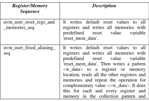
Valid register sequences are covering valid registers and memories scenarios. Generally, these sequences cover all register and memory addresses within the valid register map. Our specific valid register/memory sequences are described in the following Table I:
Table I. Valid Register/Memory Sequences
Register/Memory Sequence
Description
uvm_user_reset_regs_and _memories_seq
It writes default reset values to all registers and writes all memories with predefined reset value variable 'reset_mem_data'.
uvm_user_fixed_aliasing_ seq
issue write followed by read.
uvm_user_simple_aliasing _seq
It writes pattern value to a register and read it back, patterns are: 0x55555555, 0xAAAAAAAA, reset value and ~reset value. It does this for each and every register in the collection pattern and issue write followed by read.
uvm_user_all_register_ne gative_seq
It reads from read-only registers, writes complementary read data and then read it back. Generate UVM_ERROR if data differ from default value. It does this for each and every register read-only in the collection pattern and issue write followed by read.
uvm_user_all_register_wa lking_one_seq
Writes all bits of 1 register to 1s while the others are 0s, and issue read on all registers. Do it for all registers within the register model.
uvm_user_all_register_wa lking_userdata_seq
Writes bits of a register to 'user_walk_data' while the others are 0 (except for walking 0, others bits are 1), and issue read on all registers. Do it for all bits and registers within the register model.
uvm_user_mem_walk_bo undaries_seq
Does an uvm_mem_walk sequence on the memory boundaries space. After each boundary walk, a random memory addresses will be read.
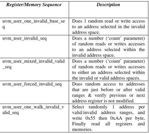
Mixed register sequences are covering both valid as well as invalid registers and memories address locations. These sequences are mainly used to test that if through Host/MCU interfaces, both valid as well as invalid address ranges of register/memory are accessed then, system will not hang and it will respond properly. Our specific mixed register/memory sequences are described in the following Table II:
Table II. Mixed Register/Memory Sequences
Register/Memory Sequence Description
uvm_user_one_invalid_base_se q
Does 1 random read or write access to an address selected in the invalid address space.
uvm_user_invalid_seq Does a number (‘count’ parameter) of random reads or writes accesses to an address selected within the invalid address space.
uvm_user_mixed_invalid_valid _seq
Does a number (‘count’ parameter) of random reads or writes accesses to either an address selected within the invalid or valid address spaces. uvm_user_forced_invalid_seq Does random access to addresses
that are just before or after valid ranges & verify previous or next address register is not modified. uvm_user_one_walk_invalid_v
alid_seq
Select randomly 1 address per valid/invalid address ranges, and write 0x55 then 0xAA per byte, Finally read all registers and memories.
Fig. 3 shows the example of a testcase based on our specific uvm_user_mem_walk_boundaries_seq sequence (as described in Table I).
Figure 3. Our Specific Memory Sequence based Testcase Example
IV. UVM REGISTER AND MEMORY APIS
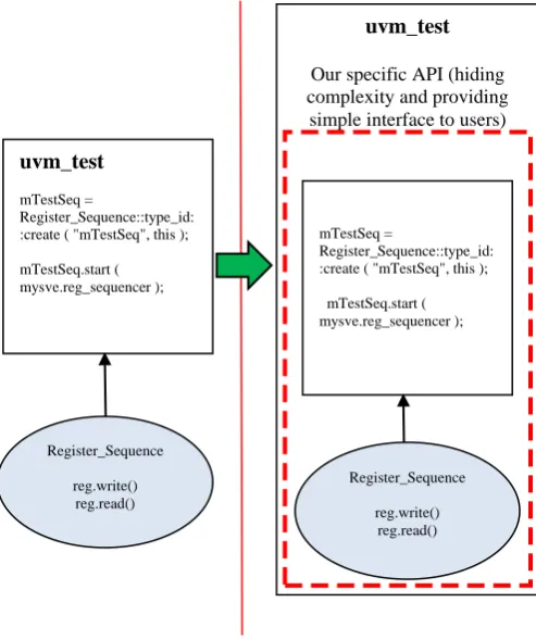
The uvm_reg package uses the well-known UVM sequence mechanism to randomize and drive register and memory sequences [1, 5]. In a sequence, we can randomly select a register object from the register model, randomize its value, set the access direction (read or write), and perform the operation. Register/memory operation sequences look much like any other UVM sequence. Using the sequence mechanism allows us to create reusable sequences to support different configuration modes. It can also use an existing sequence as a sub-sequence, traverse through all the register in the addresses range, and do much more [9, 10]. An API is provided to perform read and write operations. But read and write operations of the API can be used only in register sequence class and those operations cannot be directly used in the testcase class (derived from uvm_test class). Thus, users first need to create the register sequence classes (and sometimes virtual sequence classes also) and start them in the testcase class (derived from uvm_test class) to perform register/memory read write operations. This is complex.
Suppose now, in the testcase, a user needs to write directed values in few registers only. Creating register sequences and starting them in testcase class is a complex mechanism for users who are not expert in SystemVerilog and UVM. Thus, to avoid this complexity for users, we have developed our specific API to perform register/memory read
// --- // user_mem_walk_boundaries_seq_test
// ---
class user_mem_walk_boundaries_seq_test extends register_test; `uvm_component_utils(user_mem_walk_boundaries_seq_test) uvm_user_mem_walk_boundaries_seq mTestSeq;
function new(string name = "user_mem_walk_boundaries_seq_test", uvm_component parent);
super.new(name,parent);
set_config_string ("*.reg_sequencer","default_sequence", "uvm_user_mem_walk_boundaries_seq" );
endfunction // new
function automatic void build_phase(uvm_phase phase); super.build_phase(phase);
endfunction // automatic
extern task run_phase (uvm_phase phase); endclass: user_mem_walk_boundaries_seq_test
task user_mem_walk_boundaries_seq_test::run_phase ( uvm_phase phase ); super.run_phase ( phase );
mTestSeq = uvm_user_mem_walk_boundaries_seq::type_id::create ( "mTestSeq", this );
mTestSeq.model = mysve.regmodel;
mTestSeq.mem_range_top = 10; // Memory Top Range mTestSeq.mem_range_bottom = 10; // Memory Bottom Range mTestSeq.number_mem_access = 30; // Memory Locations to be Read
phase.raise_objection ( this ); `uvm_info (“TEST", "start reg sequence
uvm_user_mem_walk_boundaries_seq...", UVM_LOW );
mTestSeq.start ( mysve.reg_sequencer );
`uvm_info ( "TEST", "reg sequence done
uvm_user_mem_walk_boundaries_seq..", UVM_LOW ); phase.drop_objection(this);
write operations directly in the testcase class and users don’t need to write register sequences to perform register/memory read/write operations. All the complexity (like creating sequences and starting them in testcases) is part of wrapper API and users only need to call simple API directly in the testcase. Fig. 4 shows the flow to develop user specific register/memory API.
Figure 4. Our Specific Register/Memory API
In this section, we are describing how we access processor programmable registers and memories through a standard API used in test development. This API is aimed at writing simpler directed tests which require barely SystemVerilog/UVM understanding. This API can be used to facilitate dumping register access for reuse from IP to SoC, or format outputs for use in ATE test vectors development etc. In this API, basic to more complex OS based capability is provided. Our specific register APIs are described in the Table III:
Table III. Specific Register APIs
Register API Description
read_field_by_name Read register field value from
DUT by first searching register name in the register block and then, searching register field name inside the register.
rmw_field_by_name Read the register field by first
searching register name in the register block and then, searching register field name inside the register, modify it with the value and then write it in DUT.
read_reg_by_name Searching of the register name in
the register block and then, reading
its value from DUT. read_reg_by_name_a
nd_comp
Searching of the register name in the register block and then reading its value from DUT and comparing it with the expected value.
read_reg_by_address Searching of the register by its
address in the register block and then, reading its value from DUT. read_reg_by_address
_and_comp
Searching of the register by its address in the register block and then reading its value from DUT and comparing it with the expected value.
write_reg_by_name Searching of the register name in
the register block and then, writing its value in DUT.
write_reg_by_addres s
Searching of the register by its address in the register block and then, writing its value in DUT.
write_regs_using_file This API reads register names and
their values from a file. Register names and their values should be in a specific format. After reading the values from file, this API performs write operation into all the registers in DUT.
read_field_by_name_ and_comp
Searching of the register name in the register block and then, searching of register field within selected register and then reading its value from DUT and comparing it with the expected value.
read_mem_line_by_n ame
Searching of the memory name in the list of register blocks and then, reading memory line value given a memory offset from DUT.
write_mem_line_by_ name
Searching of the memory name in the list of register blocks and then, writing memory line value given a memory offset in DUT.
read_uvm_reg_by_na me
Searching of the register name in the register block and then, reading its value from uvm_reg register model (not from DUT).
write_uvm_reg_by_n ame
Searching of the register name in the register block and then, writing its value in uvm_reg register model (not in DUT).
read_uvm_mem_line _by_name
Searching of the memory name in the list of register blocks and then, reading memory line value given a memory offset from uvm_reg register model (not from DUT). write_uvm_mem_lin
e_by_name
Searching of the memory name in the list of register blocks and then, writing memory line value given a memory offset in uvm_reg register model (not in DUT).
Fig. 5 shows the usage of user API in a sample testcase example.
uvm_test
Our specific API (hiding complexity and providing
simple interface to users)
mTestSeq =
Register_Sequence::type_id: :create ( "mTestSeq", this );
mTestSeq.start ( mysve.reg_sequencer );
Register_Sequence
reg.write() reg.read()
uvm_test
mTestSeq =
Register_Sequence::type_id: :create ( "mTestSeq", this );
mTestSeq.start ( mysve.reg_sequencer );
Register_Sequence
Figure 5. Usage of User API in a Sample Testcase Example
V. ENHANCEMENTS IN THE UVM_REG REGISTER MODEL
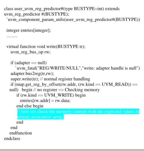
Unlike registers, memories are not mirrored because of the potentially large data space. uvm_mem doesn’t store data entries in the model. Thus, uvm_reg_predictor class is extended to check automatically memory content. Fig. 6 shows simple example of extension of uvm_reg_predictor class to support automatically checking of memory content.
Figure 6. Extension of uvm_reg_predictor class to Support Automatically Checking of Memory Content
Memory enhancement work will be continued to support huge size memories to reduce simulator memory consumption.
The current SystemVerilog implementation of the map do_bus_write() (and similarly do_bus_read()) method in the UVM register library is as described in Fig. 7.
As shown in the Fig. 7, the do_bus_write() will loop over value elements. Then in each iteration, it loops over each item address. In each inner iteration, the method creates a register transaction to be converted to bus transaction via the adapter's reg2bus() method. This technique may be suitable for low performance buses; however, it is inefficient for high performance buses as it is not utilizing bus powerful features lying underneath. Consider one scenario in our verification environment where one is operating on SPI bus and wants to do auto-increment write operation where the slave auto increments the index after each data byte. The sequential write operation is terminated with SPI_SS deassertion from the master. If user writes to a 1KB memory block; the current implementation will send 1K different bursts on an SPI bus, this looks like an inefficient way to operate on an SPI. Instead, 10 bursts (100 bytes each) could be sent, or even a single burst of 1K byte if system permits extended burst length. Each time we perform an extra operation on SPI bus, we lose at least three cycles in the case of a write operation and four cycles in the case of a read operation.
task stdAPI_test::run_phase ( uvm_phase phase ); bit [63:0] value_read, expected_val;
super.run_phase ( phase ); …….
write_reg_by_address (32'h12,32'h12345678); read_reg_by_address (32'h12,value_read); …….
expected_val = 1;
read_field_by_name_and_comp ("cropper_7bitfield", expected_val); …….
// Read Modify Write
rmw_field_by_name ("cropper_7bitfield", 7'h12); expected_val = 7'h12;
read_field_by_name_and_comp ("cropper_7bitfield", expected_val); …….
expected_val = {7'h12, 1'b0, 11'h40};
read_reg_by_name_and_comp ("cropper_enable", expected_val); …….
write_reg_by_name ("cropper_enable", 15'h1234); expected_val = 15’h1234;
read_reg_by_name_and_comp ("cropper_enable", expected_val); …….
// memories accesses
// RAM declared as 8 bit wide word, start address 'h1000, 100 words.
read_mem_line_by_name ("RAM_model", 'h90 /* offset */, value_read);
write_mem_line_by_name ("RAM_model", 'h90, 'hBEEF); // RAM is 8 bits wide - only LSB's are written
…….
// write/read of backdoor values
write_uvm_reg_by_name ("R5_4BYTES",'hFEDCBA98); read_uvm_reg_by_name ("R5_4BYTES",value);
// Write operation into all the registers in DUT using file write_regs_using_file ("RegWrites.txt");
…….
endtask: run_phase …….
Format of RegWrites.txt is described below:
### comment 1
R5_4BYTES 'hFEDCBA98 R5_2BYTES 'hBA98 REG1_LOWERPART 'hEEFF REG2_UPPERPART 'h7ABC
class user_uvm_reg_predictor#(type BUSTYPE=int) extends uvm_reg_predictor #(BUSTYPE);
`uvm_component_param_utils(user_uvm_reg_predictor#(BUSTYPE))
integer entries[integer]; …….
virtual function void write(BUSTYPE tr); uvm_reg_bus_op rw;
if (adapter == null)
`uvm_fatal("REG/WRITE/NULL","write: adapter handle is null") adapter.bus2reg(tr,rw);
super.write(tr); // normal register handling
if (map.get_reg_by_offset(rw.addr, (rw.kind == UVM_READ)) == null) begin // no register => Checking memory
if (rw.kind == UVM_WRITE) begin entries[rw.addr] = rw.data; end else begin
// here we check the memory content with the expected values in entries associative array.
Figure 7. Current SystemVerilog implementation of the map do_bus_write()
Maximizing the number of bursts may have severe consequences on simulation performance imagining a test performing hundreds of these operations. Moreover having the burst mode operation integrated in the UVM sequence API reflects more precisely the real usage of the serial bus protocol, leading to a more accurate verification of the DUT. As automatic burst handling in uvm_reg is looping through the write values, so in our verification environment, we have hacked the do_bus functions to avoid this loop.
Figure 8. Modified SystemVerilog implementation of the map do_bus_write()
As shown in the above Fig. 8, in modified SystemVerilog implementation of the map do_bus_write() method, it is not looping over data values array for UVM_BURST_WRITE kind. Burst data values are assigned to the packet of control bus UVC in the adapter.
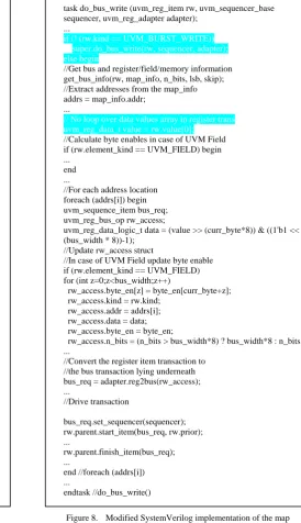
In adapter's reg2bus() method as shown in Fig. 9, uvm_reg_item is extracted and burst length is calculated using size of the data value array of uvm_reg item. Values of data value array of uvm_reg_item are assigned to the transmitter data array of master packet of SPI UVC for bus transactions.
task uvm_reg_map::do_bus_write (uvm_reg_item rw, uvm_sequencer_base sequencer, uvm_reg_adapter adapter); ...
//Get bus and register/field/memory information get_bus_info(rw, map_info, n_bits, lsb, skip); //Extract addresses from the map_info addrs = map_info.addr;
...
//Loop over data values array in register trans foreach (rw.value[val_idx]) begin
//Calculate byte enables in case of UVM Field if (rw.element_kind == UVM_FIELD) begin ...
end ...
//For each address location foreach (addrs[i]) begin uvm_sequence_item bus_req; uvm_reg_bus_op rw_access;
uvm_reg_data_logic_t data = (value >> (curr_byte*8)) & ((1'b1 << (bus_width * 8))-1);
//Update rw_access struct
//In case of UVM Field update byte enable if (rw.element_kind == UVM_FIELD) for (int z=0;z<bus_width;z++)
rw_access.byte_en[z] = byte_en[curr_byte+z]; rw_access.kind = rw.kind;
rw_access.addr = addrs[i]; rw_access.data = data; rw_access.byte_en = byte_en;
rw_access.n_bits = (n_bits > bus_width*8) ? bus_width*8 : n_bits; …
//Convert the register item transaction to //the bus transaction lying underneath bus_req = adapter.reg2bus(rw_access); ...
//Drive transaction
bus_req.set_sequencer(sequencer);
rw.parent.start_item(bus_req, rw.prior); ...
rw.parent.finish_item(bus_req); ...
end //foreach (addrs[i]) ...
end //foreach (rw.value[val_idx]) ...
endtask //do_bus_write()
task do_bus_write (uvm_reg_item rw, uvm_sequencer_base sequencer, uvm_reg_adapter adapter);
...
if (! (rw.kind == UVM_BURST_WRITE)) super.do_bus_write(rw, sequencer, adapter); else begin
//Get bus and register/field/memory information get_bus_info(rw, map_info, n_bits, lsb, skip); //Extract addresses from the map_info addrs = map_info.addr;
...
// No loop over data values array in register trans uvm_reg_data_t value = rw.value[0];
//Calculate byte enables in case of UVM Field if (rw.element_kind == UVM_FIELD) begin ...
end ...
//For each address location foreach (addrs[i]) begin uvm_sequence_item bus_req; uvm_reg_bus_op rw_access;
uvm_reg_data_logic_t data = (value >> (curr_byte*8)) & ((1'b1 << (bus_width * 8))-1);
//Update rw_access struct
//In case of UVM Field update byte enable if (rw.element_kind == UVM_FIELD) for (int z=0;z<bus_width;z++)
rw_access.byte_en[z] = byte_en[curr_byte+z]; rw_access.kind = rw.kind;
rw_access.addr = addrs[i]; rw_access.data = data; rw_access.byte_en = byte_en;
rw_access.n_bits = (n_bits > bus_width*8) ? bus_width*8 : n_bits; ...
//Convert the register item transaction to //the bus transaction lying underneath bus_req = adapter.reg2bus(rw_access); ...
//Drive transaction
bus_req.set_sequencer(sequencer); rw.parent.start_item(bus_req, rw.prior); ...
rw.parent.finish_item(bus_req); ...
end //foreach (addrs[i]) ...
Figure 9. Implementation of the adapter's reg2bus() method
Fig. 10 shows modified SystemVerilog implementation of the map do_bus_read() method. Similar to do_bus_write() method, it is not looping over data values array for UVM_BURST_READ kind. uvm_reg_item data values are extracted using get_cur_read_data function of adapter which is getting the bus value of read data from the receiver data array of master packet of SPI UVC.
Figure 10. Modified SystemVerilog implementation of the map do_bus_read()
Although some part of modified do_bus functions are specific to SPI UVC but same concept can be easily used for any other control bus UVC.
VI. AUTOMATION OF VERIFICATION ENVIRONMENT USING
IP-XACTFLOW
Even if verification engineers are familiar to write the UVM based verification environment files for verification of the IP and SoC, writing thousands of lines of verification environment code is tedious task for them. IP-XACT flow based proposed method facilitates automatic generation of UVM based verification environment files.
Accellera IP-XACT standard is used for capturing register specifications of IP and SoC [11, 13]. The code generator based on the IP-XACT accellera standard is used for generation of the SystemVerilog UVM code for the verification environment at IP level as well as for SoC level verification. Almost all devices have thousands registers
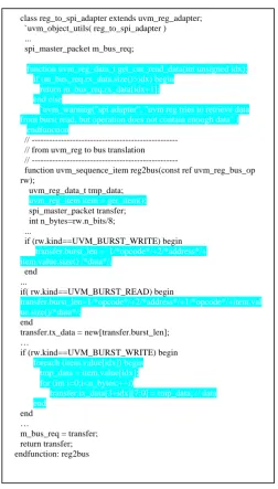
class reg_to_spi_adapter extends uvm_reg_adapter; `uvm_object_utils( reg_to_spi_adapter ) ...
spi_master_packet m_bus_req;
function uvm_reg_data_t get_cur_read_data(int unsigned idx); if (m_bus_req.rx_data.size()>idx) begin
return m_bus_req.rx_data[idx+1]; end else
`uvm_warning("spi adapter", "uvm reg tries to retrieve data from burst read, but operation does not contain enough data" ) endfunction
// --- // from uvm_reg to bus translation // ---
function uvm_sequence_item reg2bus(const ref uvm_reg_bus_op rw);
uvm_reg_data_t tmp_data; uvm_reg_item item = get_item(); spi_master_packet transfer; int n_bytes=rw.n_bits/8; ...
if (rw.kind==UVM_BURST_WRITE) begin transfer.burst_len = 1/*opcode*/+2/*address*/+ item.value.size() /*data*/;
end ...
if( rw.kind==UVM_BURST_READ) begin
transfer.burst_len=1/*opcode*/+2/*address*/+1/*opcode*/+item.val ue.size()/*data*/;
end
transfer.tx_data = new[transfer.burst_len]; …
if (rw.kind==UVM_BURST_WRITE) begin foreach (item.value[idx]) begin tmp_data = item.value[idx]; for (int i=0;i<n_bytes;++i)
transfer.tx_data[3+idx][7:0] = tmp_data; // data end
end …
m_bus_req = transfer; return transfer; endfunction: reg2bus
task do_bus_read (uvm_reg_item rw, uvm_sequencer_base sequencer, uvm_reg_adapter adapter);
…
if (! (rw.kind == UVM_BURST_READ)) super.do_bus_read(rw, sequencer, adapter); else begin
reg_to_spi_adapter spi_adapter;
//Get bus and register/field/memory information get_bus_info (rw, map_info, n_bits, lsb, skip); //Extract addresses from the map_info addrs=map_info.addr;
…
// No loop over data values array in register trans //Calculate byte enables in case of UVM Field if (rw.element_kind == UVM_FIELD) begin ...
end ...
foreach (addrs[i]) begin uvm_sequence_item bus_req; uvm_reg_bus_op rw_access; uvm_reg_data_logic_t data;
if (rw.element_kind == UVM_FIELD) for (int z=0;z<bus_width;z++)
rw_access.byte_en[z] = byte_en[curr_byte+z]; rw_access.kind = rw.kind;
rw_access.addr = addrs[i]; rw_access.data = 'h0; rw_access.byte_en = byte_en;
rw_access.n_bits = (n_bits > bus_width*8) ? bus_width*8 : n_bits;
if ($cast(spi_adapter, adapter)) begin foreach (rw.value[val_idx]) begin
rw.value[val_idx] = spi_adapter.get_cur_read_data(val_ idx); end
end …
foreach (addrs[i])
addrs[i] = addrs[i] + map_info.mem_range.stride; …
// Removal of lines where assignment to rw.value[0] was happening // when element_kind was UVM_FIELD
…
end // if (! (rw.kind == UVM_BURST_READ))
with few memories, which also need to be verified. Building register and memory model for such device is very tedious and time consuming task, building these large amounts of registers for a given model may lead to many human errors, and hence results to be inefficient.
Figure 11. IP-XACT Flow
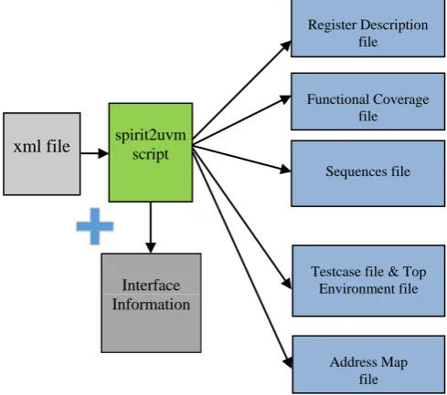
Instead we generate these register model from a specification given in .docx/.mif format which is converted to an IP-XACT standard XML format (with help of spec2spirit internal tool) as shown in Fig. 11. Various IPs are connected together to build a subsystem and various subsystems are integrated together to build a SoC. Thus, at SoC level, there is large number of IPs connected together. For each IP, register specification file in .docx/.mif format is written. Specification files of all IPs are merged together using spec2spec (Specification to Specification) script to generate XML description of the SoC level register/memory specification.
Figure 12. spirit2uvm script
This XML is then used as an input to spirit2uvm internal tool. spirit2uvm generates the SystemVerilog UVM files to build the register model [13, 16]. It also generates standard sequences such as register read-write sequence, register read sequence and register write sequence. The work of the verification engineer is simplified and bullet proof with a guarantee of 100% correctness of register model compared to the specification.
Figure 13. XML to REG_DEF File Conversion
As the specifications are also coming in a standard format, it leads to less ambiguities on writing specification of design, and hence provides higher levels of automation. spirit2uvm tool is used not only for register model and standard sequences but also for other SystemVerilog UVM files (such as test-case file, top-environment file, virtual sequence file, virtual sequencer file and address map file) used in verification of the design as shown in the Fig. 12. The Fig. 13 shows sample example of input XML file and generated output register definition (reg_def) file.
The xml file provides all the basic information
related to the IP such as IP’s base address
(<spirit:baseAddress>0x000</spirit:baseAddress>), register name (<spirit:name>MUX<spirit:name>), register field bit width (<spirit:bitWidth>4</ spirit:bitWidth>), register field bit offset (<spirit:bitOffset >0</spirit:bitOffset>), register field accessibility (<spirit:access>read-only< /spirit:access>) etc. From the given information in input XML file, corresponding register definition (reg_def) file is generated using spirit2uvm tool.
Register Description file
Sequences file
Testcase file & Top Environment file
Address Map file Functional Coverage
file
xml file
Interface Information
spirit2uvm
script
spirit2uvm spirit2uvm
spec2spec IP
Specification/ Datasheet IP
Specification/ Datasheet
IP XML Description
TOP XML Description
IP Level SystemVerilog
UVM based Verification Environment
Files
SoC Level SystemVerilog
UVM based Verification Environment
Files
spec2spirit
………
<spirit:version>0.0</spirit:version> <spirit:memoryMap>
<spirit:name>mux_address_block</spirit:name> <spirit:addressBlock>
<spirit:baseAddress>0x000</spirit:baseAddress> <spirit:width>32</spirit:width>
<spirit:register>
<spirit:name>MUX< spirit:name> <spirit:field>
<spirit:name>soft_reset</spirit:name>
<spirit:description>Soft reset of the IP</spirit:description> <spirit:bitOffset>0</spirit:bitOffset>
<spirit:bitWidth>4</spirit:bitWidth> <spirit:access>read-only</spirit:access> </spirit:field>
………
class MUX_type extends uvm_reg;
rand uvm_reg_field major_version; rand uvm_reg_field minor_version; rand uvm_reg_field patch_version; rand uvm_reg_field enable; rand uvm_reg_field soft_reset;
`uvm_object_utils(MUX_type)
virtual function void build_configuration(); soft_reset = uvm_reg_field::type_id::create( "soft_reset");
soft_reset.configure(this, 4, 0, "RO", 0, 0, 1, 1, 0); ………
VII. RESULTS AND DISCUSSION
Certain experiments are performed on IP and SoC level functional verification environment of various devices in order to assess the effectiveness of the proposed enhancements in the UVM_REG register model (user specific registers/ memories sequences, register APIs, development of IP-XACT based tools, automatically checking of memory content and improving burst handling in UVM_REG model) in terms of coverage, verification environment development time and simulation runtime.
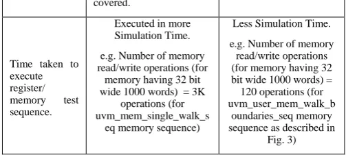
Development of user specific registers/memories sequences added more features to cover the register/memory verification corner conditions like testing the memory boundaries space, accessing both valid and invalid address ranges etc. These sequences are executed in less simulation time as compared to standard built in sequences e.g. suppose we want to perform read/write operations on SoC memory having 32 bit wide 1000 words. Using uvm_reg register
model built-in memory sequence
(uvm_mem_single_walk_seq), ~3K memory read/write operations will be performed covering full range of valid memory locations, whereas user specific memory sequence (uvm_user_mem_walk_boundaries_seq) with configuration setup of performing read/write operations in 10 upper and lower boundary locations of memory and then performing 30 random memory access operations in remaining memory locations will perform only necessary 120 memory read/write operations as covering all locations of memory is not required at SoC level.
Development of register APIs provided simple interfaces to less UVM experts. These register APIs can be directly called in uvm_test class. Enhancements in the UVM_REG register model helped to automatically check memory contents and to improve burst handling in UVM_REG model. Simultaneously, development of IP-XACT based tools helped to generate thousands of lines of code of verification environment in very short time. This resulted in significant improvement in verification quality and reduction in product verification time.
Comparison between register and memory built in sequences and our specific sequences is described in the following Table IV:
Table IV. Built in Sequences and Our Specific Sequences Comparison Table
Comparison Features
Register and Memory Built in Sequences
Our Specific Register and Memory
Sequences
Coverage of both valid as well as invalid registers and memories add- ress locations.
No specific sequence is available to cover invalid registers and memories address locations.
Users need to add dummy registers/memories models in invalid address locations in the register block to test invalid registers and memories address locations.
Corner conditions are not
Mixed register/memory sequences are covering both valid as well as invalid registers and memories locations.
All corner conditions are covered.
Executed in more Simulation Time.
e.g. Number of memory read/write operations (for
memory having 32 bit wide 1000 words) = 3K
operations (for uvm_mem_single_walk_s
eq memory sequence)
Less Simulation Time.
e.g. Number of memory read/write operations (for memory having 32 bit wide 1000 words) = 120 operations (for uvm_user_mem_walk_b
oundaries_seq memory sequence as described in
Fig. 3)
VIII. CONCLUSION
Methodology related to standard UVM register package has been studied as in [1, 15]. Register and Memory built in sequences has been studied in [3, 14]. These sequences take very long time to run at SoC level verification and don’t cover both valid as well as invalid registers and memories address locations.
This paper presented the work done in automation of register and memory models used in IP and SoC level verification, the flow, and the set of tests and APIs aimed at ensuring correctness at the 1st time on the register model, provide simple interfaces to less UVM experts or even beginners on register and memory tests development, including supporting the functional test development. Verification Environments with UVM_REG register model integrated are used to verify a variety of devices covering various protocols, applications and domains like the Internet of Things (IoT).
IX. ACKNOWLEDGMENT
The authors would like to thank Giuseppe Bonanno (Manager, STMicroelectronics), Dr. Vineet Khandelwal (JIIT, Noida) and Prof. Alka Tripathi (JIIT, Noida) for their guidance and support. We would also like to thank management and team members of Imaging Division, STMicroelectronics; Faculty members and peer scholars of
ECE Department, Jaypee Institute of Information
Technology for their support and guidance.
X. REFERENCES
[1] S. Rosenberg, and K. Meade, A Practical Guide to Adopting the Universal Verification Methodology (UVM), 2nd ed., San Jose, Cadence Design Systems, 2010.
[2] A. Jain, G. Bonanno, H. Gupta, and A. Goyal, “Generic System Verilog Universal Verification Methodology Based Reusable Verification Environment for Efficient Verification of Image Signal Processing IPs/SOCs,” International Journal of VLSI Design & Communication Systems, vol. 3, no. 6, 2012, pp. 13-25.
[3] A. Jain, and R. Gupta, “Scaling the uvm_reg model towards automation and simplicity of use,” in Proc. VLSID, Bangalore, 2015, pp. 164-169.
[4] T. Timisescu, and U. Simm, “Leveraging the UVM Register
[5] M. Litterick, and M. Harnisch, “Advanced UVM Register Modeling,” Proc. Design and Verification Conference & Exhibition Europe (DVCon Europe) 2014, Munich, Germany, 2014.
[6] S. Holloway, “The UVM Register Layer – Introduction,
Experiences and Recipes,” DVClub, 2012.
[7] A. Jain, P. K. Gupta, H. Gupta, and S. Dhar, “Accelerating System Verilog UVM Based VIP to Improve Methodology for Verification of Image Signal Processing Designs Using HW Emulator,” International Journal of VLSI Design & Communication Systems, vol. 4, no. 6, 2013, pp. 13-25.
[8] S. Iman, Step-by-Step Functional Verification with
SystemVerilog and OVM, 1st ed., San Francisco, Hansen Brown Publishing, 2008.
[9] A. Jain, H. Gupta, S. Jana, and K. Kumar, “Early
Development of UVM based Verification Environment of Image Signal Processing Designs using TLM Reference Model of RTL,” International Journal of Advanced Computer Science and Applications, vol. 5, no. 2, 2014, pp. 77-82.
[10] S. Rosenberg, “Register This! Experiences Applying UVM
Registers,” in Proc. DVCon, San Jose, 2012, pp. 1–9.
[11] A. Jain, and R. Gupta, “Unified and Modular Modeling and Functional Verification Framework of Real-Time Image Signal Processors,” VLSI Design, vol. 2016, pp. 1-14.
[12] Mentor Graphics. (2017, Jan.). UVM/OVM Cookbook.
[Online]. Available: https://verificationacademy.com/
cookbook
[13] Accellera. (2017, Jan.). Standard Universal Verification
Methodology Class Reference, Release 1.2. [Online]. Available
[14] Universal Verification Methodology, UVM 1.0, 2011.
[15] IEEE Standard for SystemVerilog-Unified Hardware Design,
Specification, and Verification Language, IEEE 1800-2009, 2009.
[16] Accellera. (2017, Jan.). Spirit information. [Online].
Available: http://accellera.org/xmlschema/spirit
Abhishek Jain received the M.Sc. degree in electronics from Delhi University, Delhi, India, in 2002 and the M.Tech. degree in computer science from IETE, Delhi, India, in 2006. He is currently pursuing the Ph.D. degree in electronics & communication engineering at JIIT, Noida, India.
He has more than 14 years of experience in industry and currently working as Senior Staff Manager at Qualcomm. He is driving key activities on functional verification flow. His current research interests include Digital Image Processing, Advanced Functional Verification Methods and System Design and Verification especially UVM based Verification, Emulation/Acceleration and Virtual System Platform. He is a member of IETE (MIETE).
Dr. Richa Gupta is a post graduate in Information Systems from Indian Institute of Technology, Kanpur and has subsequently earned her Ph.D. degree in the area of Information Theory and Coding.