University of Windsor University of Windsor
Scholarship at UWindsor
Scholarship at UWindsor
Electronic Theses and Dissertations Theses, Dissertations, and Major Papers
2011
Built-In Self-Test Solution for CMOS MEMS Sensors
Built-In Self-Test Solution for CMOS MEMS Sensors
Iftekhar Basith University of Windsor
Follow this and additional works at: https://scholar.uwindsor.ca/etd
Recommended Citation Recommended Citation
Basith, Iftekhar, "Built-In Self-Test Solution for CMOS MEMS Sensors" (2011). Electronic Theses and Dissertations. 114.
https://scholar.uwindsor.ca/etd/114
This online database contains the full-text of PhD dissertations and Masters’ theses of University of Windsor students from 1954 forward. These documents are made available for personal study and research purposes only, in accordance with the Canadian Copyright Act and the Creative Commons license—CC BY-NC-ND (Attribution, Non-Commercial, No Derivative Works). Under this license, works must always be attributed to the copyright holder (original author), cannot be used for any commercial purposes, and may not be altered. Any other use would require the permission of the copyright holder. Students may inquire about withdrawing their dissertation and/or thesis from this database. For additional inquiries, please contact the repository administrator via email
Built-in Self-Test Solution for CMOS MEMS Sensors
by
Iftekhar Ibne Basith
A Thesis
Submitted to the Faculty of Graduate Studies
through the Department of Electrical and Computer Engineering in Partial Fulfillment of the Requirements for
the Degree of Master of Applied Science at the University of Windsor
Windsor, Ontario, Canada
2011
ii
Built-in Self-Test Solution for CMOS MEMS Sensors
by
Iftekhar Ibne Basith
APPROVED BY:
______________________________________________ Dr. Nader Zamani, External Reader
Department of Mechanical, Automotive, and Materials Engineering
______________________________________________ Dr. Mitra Mirhassani, Departmental Reader Department of Electrical and Computer Engineering
______________________________________________ Dr. Rashid Rashidzadeh, Co-Advisor
Department of Electrical and Computer Engineering
______________________________________________ Dr. Majid Ahmadi, Co-Advisor
Department of Electrical and Computer Engineering
______________________________________________ Dr. H. Wu, Chair of Defense
Department of Electrical and Computer Engineering
DECLARATION OF ORIGINALITY
I certify that, to the best of my knowledge, my thesis does not infringe upon
anyone’s copyright nor violate any proprietary rights and that any ideas, techniques,
quotations, or any other material from the work of other people included in my thesis,
published or otherwise, are fully acknowledged in accordance with the standard
referencing practices. Furthermore, to the extent that I have included copyrighted
material that surpasses the bounds of fair dealing within the meaning of the Canada
Copyright Act, I certify that I have obtained a written permission from the copyright
owner(s) to include such material(s) in my thesis and have included copies of such
copyright clearances to my appendix.
I declare that this is a true copy of my thesis, including any final revisions, as
approved by my thesis committee and the Graduate Studies office, and that this thesis has
iv ABSTRACT
A new readout circuit with integrated Built-in Self-Test (BIST) method for
capacitive Micro-Electrical-Mechanical System (MEMS) devices using charge-control
method has been proposed, developed and fabricated in which the input stimuli for the
Device Under Test (DUT) is current source. A precision Time-to-Digital Converter
(TDC) is used to measure the converted time domain signals from the output of the DUT.
The proposed scheme is self-calibrated to reduce the need for external equipments and
performs well under process, supply and temperature variations. A comb drive was
designed for the simulation purpose and results indicate that the proposed method can
successfully measure and detect minor structural defects altering the MEMS nominal
capacitance. Post layout simulation was performed with the extracted view in Cadence
environment and the results were in accordance with the expectation. The proposed
design has been developed using tsmc65nm technology. The fabricated chip has been
DEDICATION
Dedicated to my respected parents whose prayers are always with me to guide,
my loving wife Israt Jahan who inspires and encourages me in every steps of my life and
my loving daughters Faiza and Fareeha whose smiles and hugs always boosts me
vi
ACKNOWLEDGEMENTS
First I want to thank the Almighty Allah for passing me through the research work
easily and allowing me to fulfil the requirements without difficulty.
Secondly, I want to thank my honourable and knowledgeable advisors, Dr. Rashid
Rashidzadeh and Dr. Majid Ahmadi for their constant support, constructive feedback and
strict guidance. Without their experience in IC design, and knowledge on SoC (System
on Chip) this project would not have been a success with the tight deadline provided by
the CMC for fabrication of the chip. I am deeply grateful to Dr. Rashid for the amount of
time he dedicated for me and this project including weekends and even the evenings and
nights of regular work week.
Thirdly, I want to thank my honourable committee members for their thoughtful
modifications and inputs regarding the thesis work during my first and second seminars.
I want to thank the CMC fabrication team for their steady and ongoing service
during the fabrication phase. Their prompt response to some of the problems I faced
while designing the chip, allowed me to proceed without any major problem.
I want to thank my colleagues and co-workers in the RCIM lab, especially
Nabeeh Kandalaft and Tareq Muhammad Supon for their valuable criticism, helpful
attitude, and strong support towards my work.
I want to mention the amount of support I received from the departmental stuffs
Andria Ballo and Shelby Marchand regarding the administrative and bureaucratic ideas.
Finally I want to thank my parents, my wife and my daughters for their
everlasting and wonderful love by supporting me in each stage of my work and cheering
TABLE OF CONTENTS
DECLARATION OF ORIGINALITY ... iiii
ABSTRACT ... iv
DEDICATION ...v
ACKNOWLEDGEMENTS ... vi
LIST OF TABLES ... ix
LIST OF FIGURES ...x
CHAPTER I. INTRODUCTION 1.1 Capacitive MEMS ...1
1.2 Built-In Self-Test for MEMS sensors ...2
1.3 My Work ...3
II. REVIEW OF LITERATURE 2.1 Built-In Self-Test ...5
2.1.1 Basic Capacitive MEMS Devices and Sensitivity BIST Method ...7
2.1.2 Symmetry BIST Method ...9
2.1.3 The Dual-Mode BIST Method ...11
2.2 Readout Circuit ...12
2.2.1 AC-bridge with voltage amplifier ...13
2.2.2 Transimpedance amplifier ...14
2.2.3 Switched capacitor circuit ...15
2.2.4 Comparison of the readout circuits ...16
III. BIST SOLUTION BASED ON CHARGE CONTROL TECHNIQUE 3.1 Proposed Block Diagram of Charge Control Method ...17
3.1.1 Charge Pump Block ...19
3.1.2 Time-to-Digital Converter (TDC) ...20
3.2 Measurement Principle and Mathematical Model ...22
3.3 Self-calibration of the BIST Scheme ...28
viii
4.2 Test circuitry and TDC schematic ...35
4.3 Schematic level simulation results ...37
4.4 Layout and fabrication of the proposed chip and post layout simulation ...40
4.5 Fabricated chip and measurement results ...48
V. CONCLUSIONS AND FUTURE WORKS 5.1 Contribution of this work...54
5.2 Future Works ...54
5.2.1 Extension of BISR to other MEMS devices ...55
5.2.2 An effective BISR technique ...56
APPENDICES “Fabrication Steps in tsmc65nm Technology” ...57
REFERENCES ...80
LIST OF TABLES
4.1 Effect of etch variations in different dimensions on measured capacitance 35
x
LIST OF FIGURES
1.1 Photo of ADXL250 accelerometer by Analog Devices Inc. 2
2.1 Basic schematic of a capacitive MEMS structure 7
2.2 MEMS structure for Symmetry test scheme 10
2.3 Fixed-plate partition for dual-mode BIST operation 11
2.4 Voltage biasing for dual-mode BIST scheme (a) Sensitivity (b) Symmetry 12
2.5 AC-bridge configuration for read out circuits 13
2.6 Transimpedance amplifier 14
2.7 Switched capacitor configuration for readout circuits 16
3.1 Simplified Block Diagram of the BIST Architecture 18
3.2 Schematic Diagram of the BIST circuitry 19
3.3 Basic time-to-digital converter using delay line 20
3.4 Timing error introduced due to noise 24
3.5 Spring-suspended model of capacitive MEMS devices 26
3.6 Electrostatic Force versus the Gap in Voltage-Control and Charge-Control
Methods 27
3.7 Delay lines configured as ring oscillators to generate time events for the TDC
calibration 30
4.1 Designed comb drive used as a DUT 31
4.2 Characteristic curve of the MEMS structure used as a DUT 32
4.3 Common fabrication faults injected in the DUT 33
4.4 The effect of one broken finger on the characteristic curve 34
4.5 Schematic view of charge pump block consisting of MEMS and reference
4.6 Employed TDC where delay lines configured as ring oscillators to generate time
events for the self-calibration 37
4.7 The schematic of each delay block 38
4.8 Relationship between capacitance variation and converted time variation 38
4.9 Successful generation of START and STOP signals in schematic level 39
4.10 Transition between flip flop 24 and 25 in TDC Vernier delay line for schematic level simulation while delay between start and stop is = 750 ps 40
4.11 Transition between flip flop 29 and 30 in TDC Vernier delay line for schematic level simulation while delay between start and stop is = 900 ps 41
4.12 Layout view of TDC single cell consisting of a MUX and one D-Flip-Flop 42
4.13 Final layout view of TDC block consisting of 32 TDC single cells 43
4.14: Complete layout view of MEMS capacitance block. START and STOP pins are
input/output pins 44
4.15 Layout view of the complete chip 45
4.16 Successful generation of START and STOP signals in MEMS capacitance block
when an external current source is supplied 46
4.17 Transition between flip flop 13 and 14 in TDC vernier delay line for post layout caliber view simulation while delay between START and STOP is = 750 ps 47
4.18 Transition between flip flop 16 and 17 in TDC vernier delay line for post layout caliber view simulation while delay between START and STOP is = 900 ps 48
4.19 Microscopic view of the fabricated chip 49
4.20 Test setup for the fabricated IC 50
4.21 Measured START and STOP signal 50
4.22 HIGH at DOUT pin and Q1 pin when START signal is HIGH 51
4.23 The measured relative delay between START and STOP signal, captured using
TDS 8000 Digital Sampling Oscilloscope 52
1 CHAPTER I
INTRODUCTION
By developing a micromachined electrostatic motor in 1987 [1], Berkley Sensor and
Actuator Center, University of California triggered a new era of Micro Electro
Mechanical System (MEMS) design. Since then, the CMOS-MEMS integration [2] has
emerged as a better mean for performance improvement of Microsystems significantly
while reducing the fabrication cost. Hence, electro-mechanical systems with analog and
digital modules are now being integrated on a single chip to produce high performance.
1.1 Capacitive MEMS
Capacitive MEMS structures have relatively simple architectures with some
added advantage over the traditional counterparts.
• MEMS devices provides high function density within a tiny space, weight
generally falls into nano-gram range.
• Due to very small sensing structure MEMS devices can achieve high resolution.
• Energy consumption is usually one tenth of the conventional devices while the
speed is ten times more.
• Signal delay can be minimized for better compatibility of its mechanical and
electrical interface.
• The fabrications cost is much lower than the conventional devices, as they can be
fabricated in batches and on the same chip with VLSI circuits.
Capacitive MEMS sensors mainly operate based on the principle of capacitance
are first converted to electrical signals by a MEMS structure and then the generated
signals are measured by a readout circuit.
1.2 Built-In Self-Test for MEMS sensors
Built-in self-test (BIST) is the technique of designing additional hardware features
into integrated circuits to allow them to perform self-testing. There are two main
techniques to conduct test on MEMS sensors: (a) voltage control and (b) charge control.
3
proposed in [4], where the central mass (movable capacitance plate) of the MEMS
structure is partitioned into two symmetrical portions. The responses of these symmetric
parts to identical stimulus inputs are captured and compared to each other. If the
difference between the responses exceeds a certain tolerance level a physical defect is
reported. This method does not require test stimulus calibration and it can detect most of
the structural defects. However, a perfect structural symmetry requirement limits the
application of this method. This method also cannot be applied to detect some global
defects affecting both sides of the symmetrical structure concurrently.
Sensitivity test method can also be used to perform test on MEMS structures [5] -
[7]. In this method, the Device Under Test (DUT) is activated to its full working range
through appropriate external test input stimuli and then the response of the DUT is
captured and compared against the signature of a fault free device. This test method can
be applied to any MEMS structure to detect possible parametric and catastrophic faults. It
is evident that precise input stimuli generator and response evaluator are required to
successfully detect DUT faults in this method, thus limiting its application for in-field
tests. In [7], the symmetry and sensitivity BIST methods are integrated in one circuit
where the fixed capacitance plate is partitioned into symmetric structure.
1.3 Proposed Work
In this thesis a new readout and built-in self-test solution for MEMS sensors is
proposed and developed which has the capability of self-calibration. In the proposed
scheme, instead of commonly used voltage controlled stimuli, charge controlled stimuli
have been employed to cover a wide range of MEMS structural defects. The proposed
hard-to-detect faults can be covered without risking the structural collapse due to
excessive electrostatic force; (b) external costly equipments are not needed for calibration
due to an employed self-calibration technique.
In the proposed test method, the Device Under Test (DUT) is charged and
discharged by current sources. This mechanism varies the electrostatic force between the
DUT plates changing the associated capacitance of the DUT. The variation in the
capacitance is captured and converted to time intervals and then digitized by a
Time-to-Digital Converter (TDC).
The rest of the thesis is organized as follows: background study and review of
literature is presented in chapter II. The block diagram of the proposed BIST circuitry
along with the functions of the building block is discussed in chapter III. Chapter III also
elaborates the principle of the proposed measurement method with mathematical
justification and the adopted self-calibration technique. Chapter IV describes the
fabrication of the DUT and test circuitry along with the schematic, post layout simulation
results and experimental measurement results. Chapter V finally concludes the thesis with
5 CHAPTER II
REVIEW OF LITERATURE
With the three-dimensional integrated circuits on the horizon, the prospect of successful
CMOS and MEMS integration has come closer to the reality. CMOS-MEMS integration
[2] improves the performance of Microsystems significantly while reducing the
fabrication cost. However, due to the multi dimensional nature [9] of such systems,
robust and advanced test methodologies are needed to address the potential challenges
ahead. MEMS sensors operate mainly based on the principal of capacitance variations
where the parameters of interest such as acceleration, ultrasonic waves and pressure are
converted to electrical signals by a variable capacitor formed by MEMS structure. The
signals generated by MEMS structure are then measured by a readout circuit. Hence, the
accuracy and resolution of readout circuits also play an important role on the overall
performance of MEMS sensors.
2.1 Built-In Self-Test
BIST circuits allow the DUT to evaluate its own quality without elaborate
automated test equipment (ATE). A BIST circuit may require little more than a power
supply and a master clock from the tester. Since the DUT testes itself using BIST, a much
less expensive ATE tester can be used. BIST have several advantages to offer:
1) It lowers the cost for testing by avoiding the need for advanced external ATE.
2) Since special test structures can be incorporated into the chips, BIST provides
3) Test times can be shortened by designing and implementing BIST techniques.
4) The consumers themselves can test chips during in-field usage.
MEMS devices are now fabricated on the same chip (SoC) with digital, analog,
memory, and FPGA circuit technologies. Hence, a thorough and effective testing solution
for MEMS devices is needed to ensure fault free functioning. However, due to the great
diversity of MEMS structures and their working principles, various defect sources and
multiple field coupling MEMS testing is very challenging [9]. Built-in self-test is
believed to be the promising solution for MEMS testing. A variety of BIST methods have
been proposed in the literature for capacitive MEMS devices.
A symmetrical test method for MEMS sensors is proposed in [4] where the
MEMS structure is partitioned into two symmetrical portions. The responses of these
symmetrical parts to identical stimulus inputs are captured and compared with each other.
When the difference between the responses exceeds a certain tolerance level a physical
defect is reported. This method does not require test stimulus calibration and can detect
most of the structural defects. However, this approach requires a perfect symmetrical
structure limiting its application and it fails to detect faults when identical global defects
exist at both sides of the symmetrical segments.
In [5] - [7] a test solution called sensitivity test is proposed. In this method, the
MEMS structure is activated to its full working range through appropriate external test
input signal. The response of the Device Under Test (DUT) is captured and compared
against the signature of a fault free device. This test method, which is similar to the
functional test of analog circuits, can be applied to any MEMS structure to detect
7
generator and response evaluator are required to successfully detect the DUT faults in
this method. Both the symmetry and sensitivity BIST methods are integrated by
partitioning the fixed capacitance into symmetric structure in [7]. However, the stimulus
input still is voltage and risk the structural collapse of the DUT.
2.1.1 Basic Capacitive MEMS Devices and Sensitivity BIST Method
A typical MEMS differential capacitance structure is shown in Figure 2.1.
Movable plate is denoted by M, fixed plates are denoted by F1 and F2, while B1 and B2
are both beams of the MEMS device. As shown in Figure 2.1, the movable plate M
constitutes differential capacitances C1 and C2 with the top and bottom fixed plates
respectively. At rest, movable capacitance is at the centre and both C1 and C2 have the
same value:
0 0
C2 C1
d A ε =
= (2.1.1)
F1
d0
C1
C2
F2 d0
B1 B2
M
Where, ε0 is the dielectric constant of air, A is the overlap area between movable and
fixed plates, and d represents the static capacitance gap between them. A vertical 0
stimulus will activate the MEMS structure and a certain displacement of movable plate M
will occur along the vertical direction. Assuming the central movable mass moves
upward with a displacement ofx, the associated capacitances C1 and C2 under the test
stimuli can be derived by
(
d x)
A − =
0 0
C1 ε (2.1.2)
(
d x)
A + =
0 0
C2 ε (2.1.3)
If V represents voltage amplitude, 0 ωdenotes the frequency and t denotes the
time then the positive modulation voltage Vmp =V0sqr(ωt) and negative modulation
voltageVmn =−V0sqr(ωt). They are applied to the fixed plates F1 and F2 respectively.
But according to the charge conservation law, charges in C1 must be equal to C2.
(
Vmp−VM)
=C2(
VM−Vmn)
C1 (2.1.4)
Solving the above equations for sensing voltage at movable plate, V we have the M
following relation:
(
x d)
V sqr( )
wtVM = 0 0 (2.1.5)
From equation (2.1.5), it is evident that the central movable plate M acts just as a
voltage divider between F1 and F2. By measuringV , we can find the displacement x of M
9
we can derive the value of the applied physical stimuli. In the sensitivity BIST mode,
driving voltage V is applied to the driving plate to mimic the action of the physical d
stimulus with electrostatic force. Then the central movable mass will experience an
electrostatic attractive force F which is expressed as: e
2 2 0 e
2 F
d AVd ε
= (2.1.6)
The response of the device to this electrostatic force is captured in the BIST mode,
measured and compared with the good device response to check whether the device is
faulty. This is the basic idea for the sensitivity test mode of a capacitive MEMS device.
However, for vertical electrostatic driving, the driving voltage cannot exceed a threshold
value called the collapse voltage by which the deflection exceeds 1/3 of the initial
capacitance gapd . Otherwise, the movable plate will collapse causing a permanent 0
damage to the structure. This is in fact the disadvantage of using voltage inputs as test
stimuli for MEMS sensors.
2.1.2 Symmetry BIST Method
For symmetry test scheme, the fixed capacitance plates are divided into
symmetrical portions. S1-S4 is fixed plates as shown in Figure 2.2. The basic idea behind
symmetry test scheme is to check whether the two symmetric capacitances that is, C1and
C2 in Figure 2.2 on the same side of the movable microstructure remain equal all the
time, after the MEMS structure is excited by input voltage stimulus. Fixed plates S1 and
S2 lie at the same side of the movable plate M. The capacitance between M and S1 is
modulated Vmp and negatively modulated V are applied to S1 and S2 separately. For mn
fault-free devices, regardless whether the movable plate is in steady state or excited, C1
and C2 remain equal. If the voltage level on M isV , the charge conservation law states M
that charge Q1 on C1 and Q2 on C2 must also be equal.
(
Vmp−VM)
=C2(
VM−Vmn)
C1 (2.1.7)
Replacing Vmp =−Vmn in equation (2.1.7), the final expression for sensing voltage is:
(
)
(
1 2)
2 1C C
C C V VM mp
+ −
= (2.1.8)
From equation 2.1.8 it is evident that when C1 equals C2, we haveVM =0. This
means if the symmetry is preserved, sensing voltage on the central movable plate is
always zero for good devices. However, if the symmetry of the device is altered due to
11
output voltage V will not be zero anymore. So, the value of output voltage on movable M
plate can easily be used as an indication of the device test result. In addition the polarity
of V can also define which side of the two symmetric structures has the fault. For M
example, a stiction defect in the right side of the mass would cause C2 to be smaller than
C1 and V will have the same phase polarity as M Vmp, and vice versa. Similar verification
can be done for both bottom capacitances C3 and C4 in figure 2.2.
2.1.3 Dual-Mode BIST Method
In the Dual-Mode BIST technique [6] for capacitive MEMS devices, the fixed
capacitance plate(s) at each side of the movable microstructure are divided into three
portions: one for electrostatic activation and the other two equal portions for capacitance
sensing. As shown in Figure 2.3, M is the movable plate, D1 and D2 are the fixed driving
plates, while {S1, S2, S3, S4} are the fixed sensing plates.
In sensitivity BIST mode, the test drive voltage V is applied to activate the DUT. d
Both the positive Vmp and negative V modulation voltages are applied to the partitioned mn
fixed plates {S1, S2} and {S3, S4} respectively (Fig. 2.4 a). The output voltage Vout of
the DUT is measured for sensitivity analysis, and then compared with pre-calculated
value within a tolerance level to determine whether the device is fault free or defective.
For the symmetry BIST mode, Vmp is applied to S1 and V is applied to S2 (Fig. mn
2.4 b). In the same manner, Vout of the movable plate is measured. A nonzero response
indicates a local defect causing the asymmetry of the DUT. An approximation can also be
made about the location of the defect based on the value and polarity of the output.
2.2 Readout Circuit
Readout circuits have been studied extensively for a long time. The principle of
capacitance-to-voltage (C-V) conversion is the dominant method to design readout
S1 D1 S2
S3 S4
Vout
D2 Vd Vmp
Vnom
Vmn
(a) (b)
13
integrated circuits (ROIC) based on the conventional Analog-to-Digital Conversion
(ADC). These circuit structures have the advantage of high Signal-to-Noise Ratio (SNR),
and high sensitivity [9] - [11]. As the supply voltage scales down, the conventional ADC
method presents some drawbacks such as high power consumption and circuit
complexity [10] - [12]. To increase the resolution, new approaches have been presented
based on the conventional Time-to-Digital Conversion (TDC).
2.2.1 AC-bridge with voltage amplifier
AC-bridge with voltage amplifier configurations [13] - [16] have a half-bridge
formed with a MEMS (CMEMS) and a reference (Cref ) capacitor, as shown in Fig. 2.5, and
is driven by two AC signals with 180 degree phase difference. The output voltage is [12]:
v p MEMS
p A
C C
C
V ×
+ ∆ =
0 , out
2
V (2.2.1)
Where, A is the amplifier gain, v V is the drive voltage amplitude,p C is the p
However, the minimum detectable capacitance is determined by the thermal noise floor
of the circuit and is still a function of parasitic capacitance [12]:
BW V
V C C
C nrms
p p MEMS
× ×
+ =
∆ ,0 ,
min
2
(2.2.2)
Where, Vn,rms is the input-referred thermal noise of the amplifier and BW is the
capacitance detection bandwidth.
2.2.2 Transimpedance amplifier
The second group of readout schemes [17] has similar configuration as ac-bridge
ones (see Fig. 2.6), except for the fact that, one resistive feedback (Rf ) is introduced, and
the drive signals need to be sinusoidal to avoid distortion. The output voltage is:
C R V fdrive m f∆
=2π
Vout (2.2.3)
15
Where, fdrive is the drive voltage frequency, ∆C =CMEMS −Cref and V is the m
drive signal amplitude. However, the poles associated withRf limits the bandwidth and
the amplifier dominant pole creates an inductive effect. The thermal noise of the feedback
resistor dominates the noise performance instead of the amplifier and the minimum
detectable capacitance is derived as follows [12]:
(
)
m amp p MEMS B V BW GBW C C T kC = + ×
∆ π 0 , min 2 2 (2.2.4)
Where, GBWamp is the amplifier gain bandwidth and kB =1.38066×10⁻²³J/K is
the Boltzmann constant.
2.2.3 Switched capacitor circuit
In the third group [12], [18] - [22] of readout circuits, an input capacitive
feedback (C ) is introduced (see Fig 2.7), which contains a packet of charge int
proportional to∆C. The minimum detectable capacitance is expressed as below [12]:
(
)
+ × = ∆ out p MEMS B s C C C C T K fCmin 1 16 2 ,0 int ×
(
BW)
(2.2.5)2.2.4 Comparison of the readout circuits
The performance of the above mentioned capacitive readout circuits were
compared using the mentioned equations. It can be said, when the parasitic capacitance is
very low then the ac-bridge circuit is able to detect very low capacitance change, whereas
if the parasitic capacitance is high, the switched capacitor and trans-impedance amplifier
circuits have better performance. Readout circuits in general should provide fine
measurement resolution. However, PVT (Process, Voltage and Temperature) variations
can affect the performance considerably.
17 CHAPTER III
BIST SOLUTION BASED ON CHARGE CONTROL TECHNIQUE
In this section, the block diagram and working principle of the proposed method will be
investigated. In the proposed test method, the Device Under Test (DUT) is charged and
discharged by current sources. This mechanism varies the electrostatic force between the
DUT plates changing the associated capacitance of the DUT. The variation in the
capacitance is captured and converted to time intervals and then digitized by a
Time-to-Digital Converter (TDC) for evaluation. The chip has been fabricated using TSMC
CMOS 65nm technology.
3.1 Proposed Block Diagram of Charge Control Method
The simplified block diagram of the proposed BIST architecture is shown in Fig.
3.1. It includes “Charge Pump” block to serve as stimulus generator and “TDC” block to
serve as response evaluator. To test a capacitive MEMS device, the MEMS structure is
stimulated by DC current sources to its full operating range and then the associated DUT
capacitor is measured to evaluate the response to the applied stimulus. The Charge Pump
block comprises two external reference current sources that forms a charge pump and
allows the scheme to perform charge-control tests on capacitive MEMS. The TDC block
includes a comparator and a Time-to-Digital Converter. The test is performed in two
phases to suppress the nonlinearity effects of the measurement circuitry. In the charging
phase, the current source I charge up the MEMS DUT capacitor until it exceeds a 1
reference voltage, where the stop signal is generated. The time interval between the start
phase, the capacitor is discharged byI , and similarly the required time is measured by 2
the TDC. This method is similar to the dual-slope measurement method widely used in
industry standard products. For I1 =I2 in an ideal case the charge and discharge time
intervals are equal however in practice due to noise and nonlinearities there is a
difference between them.
The employed dual-slope measurement technique cancels out the effects of
nonlinearities to the first degree increasing the measurement accuracy; this level of
accuracy cannot be achieved by a single phase measurement system. Moreover, as shown
in Figure 3.2, a reference capacitor is added to the proposed readout and BIST circuitry.
The addition of a reference capacitor minimizes the noise effect and the nonlinearities
associated within the readout circuit. It also minimizes the undesired effect of the
parasitic capacitance.
19 3.1.1 Charge Pump Block
The schematic diagram of the proposed circuit is shown in Figure 3.2. A reference
capacitor which is equal to the MEMS capacitor in the free standing state is included in
the circuit. The BIST scheme operates as follows. Initially, all the switchesSW ,1 SW ,2
3
SW and SW are open. First 4 SW turns on and the reference current 1 I flows in the 1
circuit. The time t required to charge the parasitic capacitance0 Cp is measured. Next
4
SW is turned on connecting Cref to the circuit. The required time t to charge up 1
Figure 3.2: Schematic Diagram of the BIST circuitry
MEMS Device
Under Test
(DUT)
1
τ
τ
1τ
12
τ
τ
2τ
21
Q
Q
2Q
nref
V
pC
refC
1I
2I
1sw
2sw
3sw
sw
4Start
p ref C
C + is measured. The required time t to charge 2 CMEMS is determined, where SW 3
is closed and SW is disconnected. 4
3.1.2 Time-to-Digital Converter (TDC)
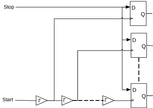
Figure 3.3 shows the basic circuit model for the Time-to-Digital converter (TDC)
designed with a single delay line including identical delay cells. The delay between the
rising edges of the start and stop signal are measured by the input of the controlled
delayed flip-flops.
The flip-flops are triggered through multi-phase clock provided to the delay line
by the applied start pulse and the number of toggled flip-flops determines the input time
interval. The delay time of one single cell limits the measurement resolution in this
scheme. However, we can design a Vernier Delay Line (VDL) using two delay lines for
higher measurement resolution. The architecture of VDL is designed in such a way, that
the delay lines produce multi-phase input signals and the flip-flops in the design act as an Figure 3.3: Basic time-to-digital converter using delay line
D
Start
Q
D Q D
Q
τ τ τ
21
arbiter to judge and compare the input signal phases and quantize the time intervals. The
delay time of a delay cell in the upper delay line (τ1) is slightly greater than that of the
lower delay line (τ2). With the START and STOP signals propagating in their respective
delay lines, the time difference between the START and the STOP pulse is decreased in
each Vernier stage byτd =τ1 −τ2, which determines the achieved resolution. The STOP
signal catches up with the START signal at position d in the delay line and gives x
information about the measured timet x
(
x)
dx d
x
t
d
d
∗
τ
<
<
+
1
∗
τ
(3.1.1)Since the delay difference between two delay elements determines the resolution,
this difference can be made much shorter than the propagation delay of a single delay
cell. In ideal case, the characteristic curve of TDC should have an identical quantization
step size over the entire measurement range. But due to noise, mismatch and random
variations of delay between delay cells or the physical length of the delay lines, in
practice the quantization step varies over the input dynamic range. Thus the characteristic
curve representing an actual TDC suffers from a non-uniform quantization step.
Deviation of step size contributes to both Differential Nonlinearity (DNL) and Integral
Nonlinearity (INL) errors. We need a proper calibration of the TDC to suppress the effect
3.2 Measurement Principle and Mathematical Model
The sensitivity of fault detection for capacitive MEMS lies in sub-fF range. To
measure such slight variations with high resolution and accuracy, noise, nonlinearities
and other source of measurement uncertainty have to be minimized. Using the
self-calibration technique for TDC, as described in [23], the undesired effects can be reduced
to a great extent by self-calibration and the measurement process justification is described
below.
When SW in Fig. 3.2 is closed, the reference current 1 I charges the parasitic 1
capacitanceCp. If the time required to charge Cp is t we can write: 0
ref p V
C t
I1∗ 0 = ∗ (3.2.1)
When SW and 1 SW in Fig. 3.2 are closed and 4 SW is open, the reference current 3
1
I charges the reference capacitanceCref +Cp. If the time required to charge Cref +Cp
is t we can write: 1
(
Cref Cp)
Vreft
I1∗ 1 = + ∗ (3.2.2)
Where, I is the constant current source and 1 Vref is the reference voltage. When
3
SW is closed and SW is open the MEMS capacitor becomes connected to the circuit 4
and charged. If the time required to charge CMEMS +Cp is t we can write: 2
(
CMEMS Cp)
Vreft
23 From (3.2.1), (3.2.2), and (3.2.3) we can write
1
1 0
1 = = +
p ref C C K t t (3.2.4) 1 2 0
2 = = +
p MEMS C C K t t (3.2.5)
Solving (3.2.4) and (3.2.5) for parasitic capacitanceCp yields to:
1 1 1 2 − = − K C K
CMEMS ref
(3.2.6)
When a MEMS sensor is activated, its capacitance deviates from the reference
value in the free standing stateCref . Assuming the change is∆C, that is
C C
CMEMS = ref +∆ and from (3.2.6) we can obtain:
ref C K K K C ∗ − − = ∆ 1 1 1
2 (3.2.7)
It can be seen that the variation of capacitance ∆C is not a function of Iref and
ref
V , hence the measurement uncertainty due to variations of these factors is significantly
reduced. Consequently, the undesired effects of process, supply voltage and temperature
variations on the measurement results are minimized. Moreover, the results obtained by
discharging the capacitors through the bottom current source I can also be used to 2
reduce the nonlinearity effects of the BIST scheme on the measurement results.
In the measurement analysis the non-ideality effects have not been taken into
consideration. In practice the accuracy and the resolution of the measurement results are
clock feedthrough and noise are among the main factors contributing to the measurement
uncertainty. Although it is possible to reduce the undesired effects of these factors by
proper circuit design techniques, in practice the minimum detectable MEMS capacitance
variation ∆Cmin is limited by noise level. To estimate∆Cmin, it is assume that the
non-ideality effects is dominated by the rms noise voltage Vn,rms of active components across
the MEMS capacitance. The total integrated noise power at the output node in figure 3.4
is given by:
2 ,
, nrms
p MEMS out
n V
C C
kT
P =
+
= (3.2.8)
Where k is the Boltzmann constant 1.38×10⁻²³J /K and T is the absolute
temperature in Kelvin.
25
The timing error due to noise, as indicated in Figure 3.4, depends on the slope of
transition and the rms noise voltage at the output. Assuming current source of I, the
output slope is given by tanα =I CMEMS +Cp and thus the timing error ∆trmscan be
determined from: rms rms n p MEMS t V C C I ∆ = + = ,
tanα (3.2.9)
From (3.2.8) and (3.2.9) the minimum timing error ∆terror can be determined as
(
C C)
IkT
terror = MEMS + p
∆ . The relation between variations of MEM capacitance
MEMS
C
∆ and time variation ∆tcan be expressed asI×∆t =Vref ×∆C. Since ∆t has to be
greater than or equal to∆terror, the minimum detectable MEMS capacitance variation can
be found from I×∆terror =Vref ×∆Cmin and can be written as:
(
)
ref p MEMS V C C kTC = +
∆ min (3.2.10)
Equation (3.2.10) indicates that the reference voltage has to be set to the highest
value to ensure maximum measurement resolution. During the test phase, when a
capacitive MEMS device is stimulated via electrical inputs, energy stored on the
capacitor must be controlled to apply electrostatic force between the capacitor plates.
This is established by one of following methods of (a) voltage-control and (b) charge
control. Due to the ease of its implementation, the voltage control method is widely
Figure 3.5 shows a parallel plate spring-suspended MEMS capacitorCMEMS. For
voltage-control methods, if the distance between the plates isd , the electrostatic force F e
between the plates can be written as,
2 2 2
2 2
1
d AV v
d C
Fe = =ε (3.2.11)
The main disadvantage of the voltage-control methods is a strong dependency
between the electrostatic force and the gap between the capacitor plates. This may lead to
permanent damage due to the collapsing of the MEMS structure. In the proposed method
using the charge-control, this dependency does not exist reducing the possibility of
structural collapse in the test phase. If the total charge stored on the capacitor is Q and
the distance between the capacitor plates isd , the stored energy W is equal to:
A d q W
ε 2
2
= (3.2.12)
Where, ε is the permittivity and
the electrostatic force
expressed as:
(
)
d d Q WFe , =
∂ ∂ =
As observed from (3.2.13), the electrostatic force
between the plates any longer, minimizing
the test phase. Figure 3.6 shows the relation between the electrostatic force in voltage and
charge control techniques.
For the spring-suspen
also be written as,
kx Fe =
Figure 3.6: Electrostatic Force versus the Gap in Voltage
27
is the permittivity and A is the plate area. The relationship between
e
F and the stored energy in charge-control method can be
A Q
ε 2
2
As observed from (3.2.13), the electrostatic force F does not depend on the gap e
between the plates any longer, minimizing the risk of MEMS structural collapse during
. Figure 3.6 shows the relation between the electrostatic force in voltage and
charge control techniques.
suspended capacitor shown in Figure 3.4 the electrostatic force can
Figure 3.6: Electrostatic Force versus the Gap in Voltage-Control and Charge Methods
The relationship between
control method can be
(3.2.13)
does not depend on the gap
the risk of MEMS structural collapse during
. Figure 3.6 shows the relation between the electrostatic force in voltage and
ded capacitor shown in Figure 3.4 the electrostatic force can
(3.2.14)
Where k is the spring constant and x is the movement of the plate in either
direction from the free standing state. Assuming the distance between the plates, d is
changed from d to 0 d0 −x due to an applied electrostatic force where d the free 0
standing distance, we can find the following expression ford :
Ak Q d k F d x d d e ε 2 2 0 0
0 − = − = −
= (3.2.15)
Using (3.2.15) and basic equation of chargeQ=CV, we can obtain the
expression for voltage across the plates:
− = − = = k A Q A d Q Ak Q d A Q C Q
V 2 2
2 0
2
0
2
2ε ε ε
ε (3.2.16)
So, equation (3.2.16) indicates that, as the gap between the plates decreases, the
capacitor voltage also decreases. This is contradictory with the voltage-controlled
methods where increase in voltage decreases the gap and eventually increasing the
electrostatic force to collapse the MEMS structure.
3.3 Self-calibration of the BIST Scheme
Proper calibration is required for the proposed BIST circuitry to minimize the
nonlinearity effects and to improve the measurement accuracy. It is shown
mathematically in equation (3.2.7) that, the change in the components of the stimulus
circuit has no impact on the measurement result and is mostly determined by the accuracy
of TDC module in the TDC block. Hence, by calibrating the TDC properly, the
measurement uncertainty can be greatly reduced. The calibration is done by constructing
29
a series of known time intervals to quantify the quantization steps representing the curve.
The TDC measurement error is approximated from the characteristic curve and
compensated.
Different TDC calibration methods described in literature [11], [23] can be
adopted, but the majority of them require precise and expensive external instruments to
perform the calibration. However, when the TDC consist of Vernier delay lines, the
calibration can be carried out through statistical methods without requiring the need for
costly external equipment [24]. For the calibration of the proposed BIST circuitry, to the
technique presented in [23] was employed. As shown in Figure 3.7, by configuring the
delay lines in the proposed TDC as ring oscillators, a set of time intervals are generated
with identical probabilities of events. These time events are then applied as input stimuli
to determine the TDC characteristic curve from the responses of these time events. To
produce proper time events for the TDC calibration and to reduce the overall delay
difference between the two delay lines additional delay cells to the feedback path of the
faster delay line are added. Upon activation of the feedback paths, the ring oscillators
start operating at close frequencies and generate evenly spread time events. If T and 1 T 2
are the periods, n is the number of delay cells in each delay line and τ1 and τ1 represent
one-cell delay in the delay lines respectively in Figure 3.6, the frequencies can be
obtained as: 1 1 1 2 1 1 τ × × = = n T f (3.3.1) 2 2 2 2 1 1 τ × × = = n T
2
τ τ2 τ2
1 τ 1
τ τ1
DUT FABRICATION AND
To evaluate the performance of the proposed BIST and readout circuitry, a MEMS comb
drive actuator was designed as a Device Under
tools. The BIST circuitry was implemented using Cadence design tools. Common
fabrication faults were then injected into the DUT and the variation in capacitance is
measured through a readout circuit.
4.1 MEMS Comb Drive (DUT)
The designed comb drive had eight fingers with a structural layer made of poly
silicon. The structure has 4 movable fingers connected to a movable arm, and 4 fixed
fingers attached to the substrate by anchors. This layout is similar to the ADXL series
accelerometers concept developed by Analog Devices Inc. [
Figure 4.1: Designed comb drive used as a DUT
31 CHAPTER IV
DUT FABRICATION AND ANALYSIS OF SIMULATION RESULTS
To evaluate the performance of the proposed BIST and readout circuitry, a MEMS comb
drive actuator was designed as a Device Under Test (DUT) using the Intellisuite CAD
tools. The BIST circuitry was implemented using Cadence design tools. Common
fabrication faults were then injected into the DUT and the variation in capacitance is
measured through a readout circuit.
ve (DUT)
The designed comb drive had eight fingers with a structural layer made of poly
silicon. The structure has 4 movable fingers connected to a movable arm, and 4 fixed
substrate by anchors. This layout is similar to the ADXL series
accelerometers concept developed by Analog Devices Inc. [3], [27]. Figure 4.1 shows the
Figure 4.1: Designed comb drive used as a DUT
ON RESULTS
To evaluate the performance of the proposed BIST and readout circuitry, a MEMS comb
Test (DUT) using the Intellisuite CAD
tools. The BIST circuitry was implemented using Cadence design tools. Common
fabrication faults were then injected into the DUT and the variation in capacitance is
The designed comb drive had eight fingers with a structural layer made of
poly-silicon. The structure has 4 movable fingers connected to a movable arm, and 4 fixed
substrate by anchors. This layout is similar to the ADXL series
designed fault-free comb drive in steady state where no electrical or mechanical forces
are applied to the structure. However, the comb drive capacitance is gradually charged up
during the test phase due to the input current stimulus. As a result, an electrostatic force is
formed between the fingers and subsequently displaces the movable arm. The entire
process changes the overall capacitance and figure 4.2 shows the characteristic curve for
such DUT. It can be seen that the capacitance varies from a minimum of 65.36 fF at the
free standing state to a maximum of 230.4 fF at the full dynamic range. The nonlinearity
between the variation of the capacitance and the distance can be attributed to the effects
of side walls and fringing capacitances.
Then some common catastrophic and parametric fabrication faults were injected
into the designed DUT to see the capacitance variation. The faults are: a) missing finger,
b) finger height mismatch, and c) etch variation as shown in Figure 4.3. Table I shows the Figure 4.2: Characteristic curve of the MEMS structure used as a DUT
C a p a c it a n c e ( fF )
Distance between the fixed and movable fingers (µm) 0.00 50.00 100.00 150.00 200.00 250.00
the simulation result of the DUT with one missing finger and its effect on the overall
capacitance of the DUT. The minimum variation of capacitance from nominal value is
3.5 fF as shown in figure 4.4.
Figure 4.3: Common fabrication faults injected in the DUT
33
the simulation result of the DUT with one missing finger and its effect on the overall
capacitance of the DUT. The minimum variation of capacitance from nominal value is
3.5 fF as shown in figure 4.4.
Figure 4.3: Common fabrication faults injected in the DUT
the simulation result of the DUT with one missing finger and its effect on the overall
capacitance of the DUT. The minimum variation of capacitance from nominal value is
Fig. 4.4: The effect of a broken finger on the characteristic curve.
0.00
50.00
100.00
150.00
200.00
250.00
1 2 3 4 5 6 7 8 9 10
(a)
(b)
0.00
5.00
10.00
15.00
20.00
25.00
1
2
3
4
5
6
7
8
9
10
E rr o r (i n f F ) C a p a c it a n c e ( fF )
Distance between the fixed and movable fingers (µm)
35 4.2 Test circuitry and TDC schematic
The test circuitry was designed using CADENCE environment in tsmc65nm
technology. As shown in figure 4.5, a library capacitor named “moscap_rf” is used for
both the MEMS and reference variable capacitors. The CNT pin controls the operational
modes of the circuit. When CNT is high, the circuit operates in the normal mode and
START and STOP signals are generated. The STOP signal is generated by charging the
MEMS capacitor with a delay ∆T equals to the charging time of the capacitor. The STOP
and START signal are fed into the TDC circuit where the stop signal operates as the
clock signal for the D-flip-flops in the TDC circuit. Two buffers to sharpen the signal are TABLE I: EFFECT OF ETCH VARIATIONS IN DIFFERENT DIMENSIONS ON MEASURED
CAPACITANCE
Etch Variation (µm)
X - Direction Y - Direction Z - Direction
Depth (µm) Measured Capacitance (fF) Depth (µm) Measured Capacitance (fF) Depth (µm) Measured Capacitance (fF) Defect-Free
65.00 65.36 10.0 65.36 40 65.36
1% 64.35 65.11 9.9 65.55 39.6 64.89
2% 63.7 64.86 9.8 65.75 39.2 64.43
5% 61.75 64.09 9.5 66.35 38 63.03
inserted before the STOP and START signals. The current is controlled by an external
resistor through the REF pin. The CREF input selects between the outputs of MEMS and
reference capacitors through the bottom MUX. The ENABLE pin is used to introduce
self-test for TDC which controls the propagation of STOP and START signals to TDC.
When ENABLE is set low the outputs from generation circuitry are not propagated
through the tri-state buffer used and STOP and START pins become input pin to test the
TDC.
The TDC consists of 32 blocks as shown in figure 4.6. Each block consists of 32
single delay elements to provide higher dynamic range in terms of detecting the time
variation. Vernier delay line is formed using D-flip-flop’s and MUX’s. The resolution is
set by the response delay of the MUX as shown in figure 4.7. After each stage, the delay Figure 4.5: Schematic view of charge pump block consisting of MEMS and reference
capacitors MEMS
C
ref
37
difference between the stop and start signal decreases. When the delay is zero, a
transition in the D-flip-flops output is set indicating the charging time of the capacitor. In
the readout mode, CNT is set to low and the DIN pin is stimulated with clock pulses to
extract the transition states of the d-flip-flop. However the DIN pin also controls the
variable MEMS capacitor by applying an external voltage and changing the capacitance
accordingly. Figure 4.8 shows the relationship between time variation ∆t in comparison
to capacitance variation ∆C. The relationship is almost linear as shown in figure 4.8.
4.3 Schematic level simulation results
Using Cadence design tool the test circuitry, charge pump block was implemented
in schematic level and simulations were performed to see the generation of START and
STOP signals as defined earlier. Please see figure 4.9. The delay is due to the charging
time of the MESMS capacitance.
Figure 4.6: Employed TDC where delay lines configured as ring oscillators to generate
Figure 4.8: Relationship between capacitance variation and converted time variation
0 20 40 60 80 100 120
0 100 200 300 400
Time (t in ns)
Time (t in ns)
39
The TDC block was also implemented in schematic level and simulated with two
deferent delays between START and STOP signals. Figure 4.10 and figure 4.11 shows
the detection of this delay in D-Flip-Flops output. First case the delay between START
and STOP signal was set to 750 ps, and second case the delay was 900 ps. From the
pre-layout simulations it is evident that the TDC is working fine in schematic level to detect
the transition for a given delay between START and STOP signals. The average delay
between the top and bottom delay lines can be approximated to 30 ps in each vernier
stage. With careful measurement it can be found that the MUX in top line adds about 26
ps delay and the D-flip flop has its own delay of around 4 ps to be added to the top delay
line. In each vernier stage the STOP signal overcomes 30 ps delay and eventually catches
4.4 Layout and fabrication of the proposed chip and post layout simulation
The proposed schematic is designed using tsmc65nm technology for fabrication.
A CADENCE design tool was used for this purpose. Appendix describes the fabrication
process elaborately. The tsmc65nm technology is a new technology adopted by Canadian
Microelectronic Corporation (CMC). Initially it seemed very hard to understand with the
limited number of resources supplied by CMC along with the kit. However, the CMC
fabrication team was very much supportive and provided with all the information needed
to complete the fabrication. This technology also provided the auto routing tool which
proved very helpful while designing the chip. At first the layout of Time-to-Digital Figure 4.10: Transition between flip flop 24 and 25 in TDC vernier delay line for
41
Converter (TDC) single cell was extracted, and tested for correct functioning. Figure 4.12
shows the layout view of TDC single cell that was the base for final TDC. However, our
TDC final block consisted of 32 such TDC single cells and the layout was also extracted
accordingly. Simulation results confirmed the TDC is working properly with given
START and STOP inputs. Figure 4.13 shows the final layout view of full TDC block. Figure 4.11: Transition between flip flop 29 and 30 in TDC vernier delay line for
Figure 4.12: Layout view of TDC single cell consisting of a MUX and one
43
Then the test circuitry for generation of START and STOP signal was extracted
for layout and simulated to see if the circuitry is functioning properly or not. Figure 4.14
shows the layout view of charge pump block with dimension 73.1 73.7 . Figure
4.15 shows the complete chip that was sent for fabrication. The total dimension for the
chip is 643.6 996 .
Figure 4.14: Complete layout view of charge pump block. START and STOP pins are
45
The full layout design for the proposed chip is then verified through Design Rule
Check (DRC) and Layout VS Schematic (LVS). Finally post layout view was extracted
and simulations were performed to compare with the schematic level results. MEMS
capacitance block was separately extracted in post layout view and figure 4.16 shows the
successful generation of START and STOP signal in calibre view. The TDC was also
extracted separately for simulation purpose and figure 4.17 and 4.18 shows the detection
of capacitance variation for two different delays as in schematic level. It is seen the
measurement delay in post layout view is higher than the schematic level and the
detection takes place in earlier stages of D-Flip-Flops.
As discussed previously, the delay between the START and STOP signals in
figure 4.16 is due to the charging time of the MEMS capacitor. This delay is then
47
Figure 4.16: Successful generation of START and STOP signals in MEMS capacitance
in the TDC block, the delay between the signals decreases. When the delay reaches zero,
a transition in the d-flip-flop is set indicating the time required to charge the MEMS DUT
as shown in figure 4.17 and figure 4.18. The difference in detecting the D-Flip-Flop
transition between the schematic and post layout design is because the resolution set by
the delay has been altered and the resolution of the TDC is set by the delay difference
between the top and the bottom lines. In schematic level it is measured to be 30 ps and
in post layout design 50 ps. This variation in vernier delay lines is due to the added
parasitic capacitance and resistance of the metal lines that are taken into consideration
when extracting the parameters for the layout simulation. Table II shows the relative
detection of capacitance variation in schematic and post layout simulation. The difference Figure 4.17: Transition between flip flop 13 and 14 in TDC vernier delay line for post
49 4.5 Fabricated chip and measurement results
The chip was designed via Canadian Microelectronic Corporation (CMC) and was
sent back to the lab by mid-July. Figure 4.19 shows the microscopic picture of the actual
fabricated chip. Some basic testing has been performed with available instruments which
showed promising results. Figure 4.20 shows the test setup with basic signal generator
and oscilloscope. According the working principle, when CNT is high, we should expect
it to be propagated to the START pin. At the same time, if reference current is supplied
the MEMS capacitor should charge to VDD and show up in the STOP pin, providing the
ENABLE pin is high. Figure 4.21 shows the measured START and STOP signal. Figure 4.18: Transition between flip flop 16 and 17 in TDC vernier delay line for post
Figure 4.19: Microscopic view of the fabricated chip TABLE4.2 FLIP
-Delay (ps) Detection in schematic Detection in Post layout
900 D29
750 D24
600 D19
450 D14
300 D09
Figure 4.19: Microscopic view of the fabricated chip
-FLOP TRANSITION IN SCHEMATIC AND POST LAYOUT SIMULATION
Detection in Post layout
Average delay in pico-seconds per stage at the schematic level
Average delay in pico-seconds per stage in post layout
D16 30 50
D13 30 50
D10 30 50
D07 30 50
D04 30 50
51
Figure 4.21: Measured START and STOP signal Figure 4.20: Test setup for the fabricated IC
![Fig 1.1 Photo of ADXL250 accelerometer by Analog Devices Inc. [3]](https://thumb-us.123doks.com/thumbv2/123dok_us/1441612.1176596/14.612.137.496.144.502/fig-photo-adxl-accelerometer-analog-devices.webp)
![Figure 2.1: Basic schematic of a capacitive MEMS structure [7]](https://thumb-us.123doks.com/thumbv2/123dok_us/1441612.1176596/19.612.181.474.410.619/figure-basic-schematic-capacitive-mems-structure.webp)
![Figure 2.2: MEMS structure for Symmetry test scheme [7]](https://thumb-us.123doks.com/thumbv2/123dok_us/1441612.1176596/22.612.163.471.76.298/figure-mems-structure-symmetry-test-scheme.webp)
![Figure 2.3: Fixed-plate partition for dual-mode BIST operation [7]](https://thumb-us.123doks.com/thumbv2/123dok_us/1441612.1176596/23.612.135.493.447.639/figure-fixed-plate-partition-dual-mode-bist-operation.webp)
![Figure 2.5: AC-bridge configuration for read out circuits [12]](https://thumb-us.123doks.com/thumbv2/123dok_us/1441612.1176596/25.612.117.534.241.411/figure-ac-bridge-configuration-read-circuits.webp)
![Figure 2.6: Transimpedance amplifier [12]](https://thumb-us.123doks.com/thumbv2/123dok_us/1441612.1176596/26.612.116.525.440.643/figure-transimpedance-amplifier.webp)
![Figure 2.7: Switched capacitor configuration for readout circuits [12]](https://thumb-us.123doks.com/thumbv2/123dok_us/1441612.1176596/28.612.118.515.76.262/figure-switched-capacitor-configuration-readout-circuits.webp)