Nanoglasss: Present Challenges and Future Promises
M. R. Sahar
a*and S. K. Ghoshal
bAdvanced Optical Materials Research Group, Department of Physics, Faculty of Science Universiti Teknologi Malaysia, 81310 UTM Skudai, Johor
mrahim057@gmail.coma*, Sibkrishna@utm.myb
Keywords: Nanoglass, nanophotonics, surface plasmon, plasmonics, fluorescence, up-conversion, SERS.
Abstract. This presentation provides a panoramic overview of the recent progress in nanoglass plasmonics, challenges, excitement, applied interests and the future promises. A glimpse of our gamut research activities with some significant results is highlighted and facilely analyzed. The term 'nanoglass' refers to the science and technology dealing with the manipulation of the physical properties of rare earth doped inorganic glasses by embedding metallic nanoparticles (NPs) or nanoclusters. On the other hand, the word 'plasmonics' refer to the coherent coupling of photons to free electron oscillations (called plasmon) at the interface between a conductor and a dielectric. Nanoglass plasmonis being an emerging concept in advanced optical material of nanophotonics has given photonics the ability to exploit the optical response at nanoscale and opened up a new avenue in metal-based glass optics. There is a vast array of nanoglass plasmonic concepts yet to be explored, with applications spanning solar cells, (bio) sensing, communications, lasers, solid-state lighting, waveguides, imaging, optical data transfer, display and even bio-medicine. Localized surface plasmon resonance (LSPR) can enhance the optical response of nanoglass by orders of magnitude as observed. The luminescence enhancement and surface enhanced Raman scattering (SERS) are new paradigm of research. A thumbnail sketch of the fundamental aspects of SPR, LSPR, SERS and photonic applications of various rare earth doped/co-doped binary glasses containing metallic NPs are presented. The recent development in nanoglass in the context of Malaysia at the outset of international scenario is projected.
Introduction
Research in nanoglass (glass containing metallic NPs) is highly fertile with several ramifications for future technologies. The term nanoglass and plasmonics go hand in hand. Plasmonics exploits the collective oscillations of conduction electrons in metallic nanostructures called plasmons, excited by the incident electromagnetic waves. Surface plasmons (SPs) are the light-induced excitations of electrons on metal surfaces or metal dielectric interfaces [1]. The excitation of SPs by light is at precisely matching frequency is known as ‘surface plasmon resonance’ (SPR) for planar surfaces or ‘localized surface plasmon resonance’ (LSPR) for nanometer-sized metallic structures [2-4]. This phenomenon is the basis of many standard tools for measuring adsorption of material onto planar metal (gold and silver) surfaces or onto the surface of metal nanoparticles (NPs). It is the fundamentals behind many color based biosensor applications and different lab-on-a-chip sensors [1-8]. Therefore, stimulating the surface plasmons of NPs inside the glassy matrix is the essence of nanoglass plasmonics.
Interestingly, enhancing the absorption and emission cross-section of rare earth doped inorganic glasses by means of embedding metallic NPs with controlled sizes is challenging [9-11]. The luminescence quenching in glasses is detrimental unless strategically inhibited via NPs embedment. The SPs can pick up more light and carry it along the metal surface for comparatively large distances. Using plasmons light can not only be focused into the tiniest of spots but can also be directed along complex circuits or manipulated it many different ways. It is possible to achieve all of this at the nanoscale that is several orders of magnitude smaller than the wavelength of light. This nanoscale is far below the resolution limits of conventional optics often called sub-diffraction limit.
Since the inception of surface plasmon optics there is a rapid transition from fundamental research to more applied oriented research and nanoglass is one of the emerging materials. These developments have led to the notion of plasmonics, the science and technology of metal-based optics and nanophotonics [3, 4]. It is well known fact that electronics is the aspect ratio and is limited in speed, whereas, photonics is the diffraction that is limited in size. Plasmonics can go beyond the sub-diffraction limit and is not limited my any means because the SP wavelengths can reach to nanoscale at optical frequencies [3]. Plasmonics will enable an improved synergy between electronic and photonic devices by naturally interfacing with similar size of electronic components and similar operating speed photonic network, and hence the new concept ‘plasmo-electronic chip’ is introduced [4]. Observation of birefringence, superparamagnetism, high field irreversibility, high saturation field and other nonlinear behaviors has added extra impetus in magnetic nanoglass research.
Rapid progresses in materials synthesis and nanofabrication techniques over the last decade have led to variety of applications of plasmon-assisted nanophotonics such as, high-resolution plasmon printing, laser shaping, solar concentrators, nanoscale waveguides, sensing, bio-detection at the single-molecule level and enhanced transmission through sub-wavelength apertures, to cite a few. However, in the miniaturization of photonic circuits, it is now being realized that the metallic structures can provide unique ways of manipulating light at length scales smaller than the wavelength. The optical manipulation of micron/submicron sized particles and bio-molecules are investigated through plasmonics. Some of the interesting phenomena in nanoglass plasmonics are:
• Generation of the surface plasma waves inside inorganic glasses and the dependence of plasmon resonance on metal particle size and topology and nature of RE ions,
• Enhancement of the electromagnetic field close to metal NPs, especially SERS and metal enhanced fluorescence (MEF),
• Effects of the metal nanoshells on plasmon resonance,
• Influence of metal surface on radiative and nonradiative decays of RE, and
• Fabrication of plasmonic solar cells using nanoglass.
The recurring theme of this presentation is to address some of the following relevant issues in nanoglass:
• What is nanoglass plasmonics?
• How to fabricate nanoglass materials for plamonics applications?
• Why research is necessary in nanoglass?
• What is the present status for commercialization?
• Why research in nanoglass so interesting?
• What are challenges and difficulties in nanoglass research?
• How promising are they for future technology?
This review is organized as follows. In Section 2, a birds’ eye view of the research background with recent development in nanoglass and its future prospects are presented. Few important results from our group are highlighted in Section 3. The recurring theme of Section 4 is the main challenges ahead. Section 5 describes the possibility of widespread exciting applications and the need of further research. Conclusions and further outlook are summarized in Section 6.
Background
origin of such colors of dispersion using Maxwell’s theory of classical electromagnetic radiation in which the phenomena was attributed to strong absorption and scattering of light by dispersion of metal NPs [6].
However, in the nanotechnology era there are renewed interests on metal nanostructures and metal-dielectric interfaces. During last two decades a series of noble-metal particles are fabricated using advanced nanotechnology route showed a strong absorption band in the visible region of electromagnetic spectrum, arising from a resonance between collective oscillations of conduction electrons with incident electromagnetic radiation. Consequently, scientists are interested to guide, manipulate and control such strong absorption band associated with plasmon and hence the genesis of plasmonics [3] and latterly nanoglass plasmonics. Gold and silver are well known for their unique plasmonic and electronic structure properties with wide optical tenability and bio-compatibility [8].
The theory of plasmonics mainly concerned with the origin and the tunability of the strong absorption band from metal nanostructures in the visible region as a function of shape and size of NPs. A change in the shape of NPs produces more profound effect on the SPR band and causes much larger shifts compare to the change in size of the NP. The extinction coefficient or the cross-section that depends on the combined effects of the absorption and the scattering cross-cross-sections is a useful parameter for SPR to occur in metal nanostructures [7]. It is this property that is exploited in nanoglass. The ratio of extinction cross-section to the effective cross-sectional area known as the extinction efficiency is a measure of the SPR. The SPR can be propagating or localized in nature with varying SPR bandwidth and peak position depending on the size, shape and geometry of nanostructures. The theory based on the electric-dipole approximation is too simple and therefore, unable to explain the detail nature of the SPR band as a function of NP size, and requires modification. A much rigorous and complex theory called discrete dipole approximation that is developed to get better understanding of the experimental observations [11]. The modified theory considers the NPs size dependent relative permittivity by assuming that the particle size is smaller than the mean free path of conduction electrons [10-13].
Nanotechnology has shown immense promise of synthesizing noble materials with remarkable optical and electronic correlation effects [14-17]. The density of the electronic states and dielectric confinement in materials containing noble metallic NPs make them venerable with unique optical, electronic, thermal, magnetic and chemical properties [17, 18]. Introduction of the metallic NPs in the bulk glass is gaining ever growing demand due to their industrial and technological applications. The glass nanocomposites containing metallic nanoparticles are among the splendid technological materials due to their potential solicitations as photochemical material, multi-dimensional objects in colorful industrial art-jobs, non-linear nanophotonics fabrics, memory devices and optical switches to cite a few [19-21].
Combining the gifted glass properties such as high transparency, simple methodologies for syntheses, large intake of RE ions and mechanical strength to the noble features of metal NPs, innovative composites and ceramics can be developed where the NPs are protected from air oxidation and other environmental effects. One of the fascinating areas in nanoglass plasmonics is surface-enhanced Raman spectroscopy. One can enhance the signal by several orders of magnitude larger and is strong enough to detect a single molecule. The surface-enhanced Raman spectroscopy is very useful in the biochemical and materials sciences for providing information on the chemical composition of molecules at very small concentrations and detail microstructures. Surface-enhanced Raman spectroscopy is a plasmonic effect in which silver/gold NPs act as nanontennas to gather the incoming laser light and, through their SPs, concentrate it.
the dielectric host is more effective in presence of non-spherical NPs such as elliptical, bipyramid, nanorods etc. Malta et al. [23] reported the large enhancement of the Eu3+ luminescence intensity in the borosilicate glass mediated by small silver particle. Som and Karmakar prepared core-shell (silver-gold) binary-NPs embedded antimony nanocomposites [24], where large luminescence enhancement of the Nd3+ ion is explained in terms of LSPR on the fluorescence of RE. The enhancement of the Eu3+ ion luminescence intensity in the presence of gold NPs in tellurite glass is observed by Almeida et al. and Rivera et al. [25, 26]. We examined the effect of silver and gold NPs on the up-conversion emission of the Er3+-doped zinc-tellurite, magnesium-tellurite, sodium-tellurite and phosphate glasses [27-29].
The term nanoglass plasmonics is coined due to the distinctive characteristics of resonant absorption displayed by different glasses when nano-sized structures (usually metals or semiconductors) are incorporated [30-32]. It is well known that emission and absorption cross-sections for RE ions are small that needs to be enhanced for widespread applications. One strategy is to co-dope with another rare-earth (RE) like Er3+ [33], the other is to embed with semiconductor nanostructures like Si [31] and more lately embedding metallic NPs like Ag or Au [34-37]. These metallic NPs so called plasmonic nanostructures when located within the vicinity of the RE ion can enhance the luminescence yield by several order of magnitude due to the local field effect (LFE) induced by SPR [38, 39]. This mechanism is known as metal enhanced luminescence (MEL) which is a powerful tool not only in biotechnology [38, 39] but also in the novel field of nanophotonics [40]. Despite few studies, the influence of metallic NPs on the spectroscopic properties and the mechanism of improved optical response are far from being understood.
The radiation emitted by fluorophores into free space can be modified via the existence of small metallic NPs that causes remarkable optical alteration. Surprisingly, there may be increase or decrease in the radiative decay rates of fluorophores due to metal surfaces which can enhance the rate of resonance energy transfer [41, 42]. SP interacting with excited fluorophores can induce transforming effect on them. The interaction between fluorophores and metal is referred as metal-enhanced fluorescence (MEF) in the field of biotechnology. In telecommunications, the optical signal used for data transfer through optical fibers often gets attenuated due to scattering, absorption, dispersion and impurities. To overcome these problems erbium doped fiber amplifiers were developed and Raman amplifier utilizing stimulated Raman scattering is employed [43-44]. Our domain of interest in nanoglass is to investigate the effect of SPR of metallic NPs on the optical properties such as absorbance, photoluminescence and Raman in RE doped/co-doped glasses.
Rare earth (RE) doped tellurite glasses are known as promising materials for transmission windows, optical fibres and solid state lasers, to cite a few [45-48]. By changing the structure and the neighboring states of doping ions, the emission characteristics of lasing glass might be achieved [47]. The incorporation of metallic NPs in glass matrix has generated great interest due to the potency to enhance their structural and optical behaviors [48-59]. Interestingly, glass is an excellent medium for growing metallic NPs [50]. Metallic NPs exhibit unique optical, electronic, magnetic, chemical and thermal properties due to their modified electronic density of states, the effect of quantum as well as dielectric confinement [51]. The strong dependence of electronic properties of the glass materials on the size and shape of NPs are reported [52, 58]. The interaction and contribution of metallic NPs in glass matrix in enhancing the optical properties are investigated by Som et al. [59]. It is believed that controlling the size of NPs in glass matrix by the process of heat treatment (annealing) and optimizing the RE ions concentration collectively an excellent optical performances of tellurite glasses can be achieved in a tunable manner.
will perhaps overcome this problem. Nevertheless, continual research in nanoglass is breeding more research.
Significant Results
The enhancement of the up-conversion luminescence efficiency of several orders of magnitudes is exploited by introducing metallic NPs in REI doped glasses. The enhancement is subjected to the condition that the wavelength of the excitation beam or the luminescence is near to the SPR wavelength. Enhancement of the luminescence of REI such as, Eu3+, Er3+, Tb3+, Yb3+ and Sm3+ is observed in varieties of glasses containing silver, gold and other NPs. This enhancement is attributed to the strong local field or energy transfer effects on the ions located in the proximity of the NPs that change the luminescence of REI doped glasses. Interestingly, this new approach to increase the luminescence by several folds in REI doped glass is receiving renewed attention due to the large interest in plasmonics based nanophotonics. The increment of nanocrystal (called NPs) grain size can cause more defect centers and stronger lattice deformation at the interface of the metal nanocrystals, which broadens the absorption tail and red shifts the band gap. The band gap red shift increases the two photon absorption coefficient and decreases the optical limiting threshold. The third-order nonlinear susceptibility can be enhanced for the transient polarization of the trapped state electrons on the surface of the metallic nanocrystals [26, 27].
In the past, tellurite and phosphate glasses, with its excellent optical properties, chemical durability and thermal stability, is extensively investigated aiming at their applications in the development of prospective photonic devices [27]. In particular, the rapid development of ultrafast all-optical devices gives rise to strong interest in optimizing their nonlinear optical properties of the nanoglass by doping with heavy-metal oxide or rare earths. It is realized that, the magnitude of the third-order nonlinear susceptibility can be enhanced by modifying the local structure of these glasses through the incorporation of metallic NPs. Such a glass doped with ZnO NPs exhibits distinct optical bi-stability and it acts as an excellent broadband saturable absorber doped with cobalt NPs or an optical power limiter doped with erbium.
Some external fields, such as electric, magnetic and optical fields can be applied to control the nucleation and crystallization of nanocrystals crucial for enhancements in physical properties. It is important to control the growth of nanocrystals in the desired local areas when preparing nanocrystal patterns in glass substrates. The quantum effect of nanocrystals is a crucial factor to improve nonlinear optical performance of nanocrystal embedded glasses, while controlling the size distribution and content of nanocrystals in the glass accurately is a key to obtain good quality. In order to improve optical nonlinearity to a big extent, various NPs, such as Au, Ag, AgCl, AgO, CuCl, CdS, CdSe, ZnO and CdTe are introduced into optical glasses through heat treatment, porous glass, ions injection, ion exchange, sol-gel methods etc. When the size of NPs embedded in the glass is less than their critical Bohr radius, the NPs play an important role in improving optical nonlinearity greatly. For gold NPs hosted in different glasses the SPR is found to be located in the green-yellow region with tails in the blue and red regions. Depending upon the distance and geometry, metal surfaces or particles can result in quenching or enhancement of fluorescence. Hence, it is concluded that the increase in REI luminescence is due to local field enhancement, and is mainly attributed to the difference between the dielectric functions of the gold NPs and the host glass. This may find useful applications in biophotonics.
Surface plasmon resonance (SPR) is the basic concept of plasmonics which describes the interaction of the light with metallic surface. Oscillations of electronic cloud of metallic NPs when excited by the light with wavelength larger than the size of particles results strong field around these nanostructures. Firstly, the excitation is enhanced by the large localized electric field between two NPs that leads to an enhancement of the Raman modes of probing molecule by a factor of η2, where η is the enhancement factor. The emitted Raman signals further experience an enhancement by the same SPR effect. Therefore, output Raman signal is enriched by a factor of η 4 [66]. The maximum enhancement happens near the plasmon frequency [67, 68]. Even if, the plasmon resonance may not be efficient in special cases but LRE allows the confinement of large electric field in the sharp edges or at curved surfaces of metals.
The dielectric hosts with high nonlinearity render better confinement of localized field. Therefore, SPR is recently been exploited to enhance the fluorescence from rare earth (RE) doped heavy metal glasses. The enhancement of emission intensity in Eu3+-doped silicate glass by embedding silver particles is reported by Malta [23]. Recently, numerous efforts are dedicated to increase the luminescence intensity of Er3+ [69], Sm3+ [70], Pr3+, Tm3+, Eu3+ and Nd3+ [71] doped glasses via the incorporation of noble metallic NPs (Au and Ag). The reactivation of Raman signals in Ag NPs–deposited thin films on silicate glass substrate displayed order of magnitude enhancements of Raman scattering attributed to the SP excitation of silver particles [43]. Upender et al. [73] demonstrated that the enhancements of Raman signals by Ag nanoclusters deposited on glass substrate is higher than p-type Si(100) substrate. The theme of sensing using plasmon resonance spectroscopy and more recently via SERS received paramount importance in plasmonics [78-82]. The SERS phenomenon was first observed by Fleischman et al. [60], the mechanisms were explained later using electromagnetic enhancement [74] and chemical enhancement (charge transfer) [75]. These theories being complementary rather than exclusive interpretations of the SERS phenomena still persist.
The origin of the SERS is still debatable. SER-based sensors employ a rough metal surface as a substrate. Substrates including roughened noble metal films and lately nanostructured surfaces such as NPs, nanodisk and nanotriangle arrays are exploited. When the metal nanostructures are irradiated by a laser in resonance with the characteristic frequency of the material (viz. 633 nm for bulk Au), plasmons are generated around the nanostructure. It is the plasmon that gives rise to a significant enhancement in the local electric field around the nanostructure, which in turn amplifies the Raman modes of the molecule being studied. SERS is essentially recognizes as plasma effect due to its reliance on plasmons. An analytical expression for the SERS enhancement factor is derived by Willets et al. [76] and Ru et al. [77].
Pan et al. [78, 79] studied the effect of the silver NPs on the spectroscopic properties of the erbium doped chalcognide and observed enhanced excitation, luminescence and high quality Raman signals (SERS). An enhancement of the Raman signal up to few times accompanied by red-shift in erbium doped zinc tellurite glass containing Ag NPs is recently observed by us [80, 56]. We use melt quenching method to prepare all nanoglass samples with appropriate composition and optimized steps. The characterizations are made by using XRD, FTIR, EDX, HRTEM, FESEM (structural), DSC and DTA (thermal) and UV-Vis absorption, PL and Raman (optical). The sizes of NPs growth are controlled via heat treatment temperature and time (annealing). Alteration of annealing time and AgCl concentration modified the optical properties. It is known that as the inter-particle spacing becomes smaller, interactions (efficient surface plasmon coupling) between the closely spaced metallic NPs significantly generates enhanced localized electric field hence luminescence intensity can be increased by many folds.
concentration of Ag and maximum annealing time above glass transition temperature several NPs approach closely or coalesces (Ostwald’s ripening), so that their induced electric fields are expected to overlie and produce “hot spots” regions (or the regions of stronger electric field) that leads to a stronger surface enhanced fluorescence. A Gaussian size distribution of the NPs with narrow FWHM is often achieved and the obtained average diameter of NPs ranges from 5-50 nm. The increased average size of NPs through the introduction of AgCl is attributed to the heat treatment driven growth via two mechanisms (fig. 1) (i) Ostwald ripening, where atoms or small clusters of atoms diffuse from smaller to larger NPs, and (ii) nanoparticle migration followed by coalescence at higher concentration of silver NPs.
Fig. 1: (A) Ostwald ripening (B) nanoparticle migration followed by coalescence.
The Raman spectra shown in Fig. 2 comprised of three peaks centered at 280, 366 and 603 cm-1 belongs to the linkages in the bulk matrix that show maximum enhancements of 8.62, 8.29 and 8.18 times, respectively, attributed to the SPR contribution which enlarges the local electric field. The increased concentration of silver NPs intensified the Raman signal, while the growth of NPs due to annealing contributed to further enhancements in the local field and Raman intensity. In addition, the observed red-shifts of all peaks ascribed to the closeness of excitation wavelength and SPR frequency is quite interesting and relatively new. The peaks around 713 and 747 are assigned to stretching vibrations of TeO3/TeO3+1 unit [82], and the peak at around 603 cm-1 originated from
TeO2 units [83]. In the lower frequency, the peak at 286 cm-1 is assigned to both TeO3 tp and Er–O
bond [84], and the peaks around 336, 367 are assigned to Zn-O [85].
Fig. 2: Raman signals of the samples ExAyHz, where x=1mol% is the concentration of erbium ions, y=0, 0.5, 1 and 2 mol% is the concentration of the AgCl, and z=0 and 8 is the annealing time
for the zinc-tellurite glass.
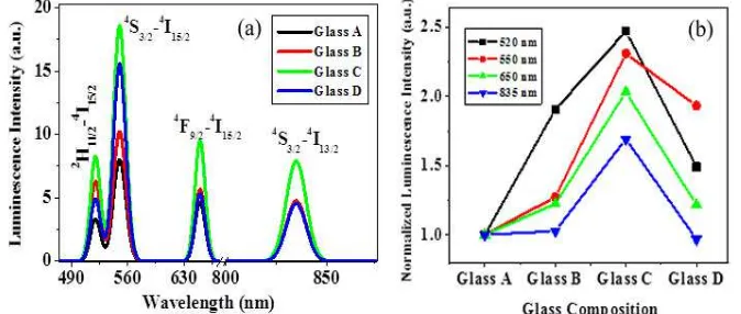
Fig. 3(a) displays the PL spectra of the studied glasses that exhibits four prominent emission bands centered at 520 nm, 550 nm, 650 nm and 835 nm attributed to 2H11/2→4I15/2, 4S3/2→4I15/2, 4
F9/2→4I15/2 and 4S3/2→4I13/2 transitions, respectively. All the bands are enhanced significantly by
factors of 2.5, 2.3, 2 and 1.7 times, respectively (Fig. 3(b)).
Fig. 3: (a) Luminescence spectra of glasses under an excitation of 786 nm i) Without AgCl (A), with ii) 0.1 mol% (B), iii) 0.5 mol% (C), iv) 1.0 mol% (D) AgCl (b) plot of emission intensity versus concentration of Ag (mol%). Maximum amplification for the green and red bands occurred
for 0.5 mol% Ag.
The metallic NPs result in gigantic and highly localized electric field around the Er3+ ions [30-33]. As, surface plasmon polariton generated by SPR move along the surface of metallic NPs focus light in the sub-wavelength structures due to the difference in relative permittivity of the surrounding host and metal. Furthermore, the local field around the metallic NPs is enhanced by the concentration of light and metallic screening (LRE) with respect to the incident field [34, 35]. Nevertheless, metallic NPs offer a unique prospect of modification of fluorescence due to changes in the rates of excitation and emission of lanthanide ions. If the host is a glass then the effect of metallic NPs on the emission and absorption rates of lanthanide ions is primarily of electronic origin [36, 37]. It can be visualized as an added interaction in the proximity of metallic NPs generated by plasmonic excitation at the Mie resonance frequency [36, 37]. Similar mechanism is also responsible for the enhancement in the down-conversion.
The partial energy level diagram of erbium ion as presented in figure 4 is instructive for explaining the luminescence processes and observed enhancements. Even though enhanced quantum yield is desirable, however, both enhancement and quenching of fluorophore is observed near the metallic NPs [38, 39]. If the distance between metallic NP and fluorophore is 50 Å or more then enhancement in fluorescence can be achieved [37]. Enhancement in fluorescence can be maximized in some regions near metal surface due to the exponential decrease of the local field from the surface [35, 37]. Ground state absorption (GSA), excited state absorption (ESA) and energy transfer up-conversion (ETU) are the vital involved mechanisms which can be explained as follows
4
I15/2→4I9/2 [GSA] → 4I11/2 [NR] → 4
F7/2 [ESA] →2H11/2 [NR] →4S3/2
where NR is the non-radiative decay. The ETU steps are (Fig. 4(a)): (4I11/2, 4I11/2) → (4I15/2, 4F7/2)
(4I11/2, 4I13/2) → (4I15/2, 4F9/2)
reaffirm that the overall enhancement in the emisission bands of Er3+ is due to the sum of the following two processes:
• Local field effect around the rare-earth ions
• The energy transfer from fluorescent Ago → Er3+
At maximum concentration of AgCl (1.0 mol%), a quench is observed in both up and down conversion fluorescence intensity. The reason for quenching is the energy transfer from Er3+ ions to silver NPs (Er3+→Ag0) and reabsorption by SPR for increased quantities of silver NPs having a plasmon absorption band range extended over the emission peak position of Er3+[40, 41].
Fig. 4: (a) Partial energy level diagram of Er3+ ions in zinc-tellurite glass showing up-conversion emissions at 520, 550 and 650 nm via GSA, ESA and ET between two Er3+ ions. Local field effects due to silver NPs are also shown. (b) Partial energy level diagram for down-conversion emission
along with local field effects due to silver NPs.
The schematic for the interaction of the indicent light coupled by Er-Ag and the visible emissions of the rare earth is presented in Fig. 5. We provide a mechanism for the observed luminescence enhancements and SERS are in conformity with others. Our results suggests that these nanoglasses can be nominated for nanophotonic applications.
Fig. 5: Red and green emissions from Er3+ under an excitation of 786 nm.
Present Challenges
Nanoglass plasmonics has the potential to improve photonic products in a wide array of new applications. There are no yardsticks or a clear roadmap yet regarding the stability, efficiency, tolerances, longevity and large-scale production. However, the promises of technologies and applications are diverse and multidisciplinary, in early stages of development, and the opportunities are spread throughout the value chain. There are different challenges of nanoglass research and some of them are:
• Designing nanoglass chip and solar concentrator
• Market strategy
• Single–molecule addressing (pre-requisite for architectures work)
• Testing for solid state lasers and display devices
• Growing nanowires, nanobelts, NPs, nanorods and nanoarrays in a tunable way inside the glass matrix, glass ceramics and nanocomposites
• Identifying hierarchy of interactions with other quasi particles of magnetic and semiconducting types
• Improving enhancement and gain
• Integration, costs, standards and safety etc.
Although, these are the main challenges but the following are expected benefits from nanoglass which will bridge the gap between current photonic systems and future approaches bringing in example:
• Access to further integration
• Mass production techniques and accurate fabrication
• Plasma-electro integration
• Cheaper and efficient devices
• Will dissipate less energy, occupy less volume, require lower input signal
• Will probably rely on self-assembly, be more lasting
• Will be more flexible and sensitive
Majority of the present fabrication and characterization techniques are based on expensive technologies and processes belonging to the very high technology pursuits at an expensive category. There is great interest and need for approaches as well as strategies for large-scale production, which are more cost-effective and environment friendly. The criteria on tolerances, efficiency of energy transfer and longevity are other significant issues that manufacturer have to meet when it comes to material purity because this will be an important cost factor for lateral size control.
Applications
Nanoglass plasmonics is a unique field because it combines scientific challenges with large variety of near-term applications. Fundamental research in nanoglass leads to applications in communications technology, lasers, solid-state lighting, bio-labeling, solar concentrator, data storage, lithography, biosensors, optical computers, imaging, solar cells, light-activated medical therapies, displays, magneto-optic devices and smart materials to cite a few [1-4, 12]. Some of the important areas that will find large market in next ten to fifteen years from now are identified. Many futuristic applications regarding plasmonic materials rendering invisibility are also inspiring researchers. SPPs can be tightly bound to the metal surface, penetrating ~100 nm into the dielectric and ∼10 nm into the metal. This feature implies the possibility of using them for miniature photonic circuits and optical interconnects and has attracted a great deal of attention to SPPs. Applications of SPs in solid-state lighting and lasing are just appearing, but it may be that traffic lights are composed of SP light emitting diodes in a few years time!
Surface plasmon in lanthanides doped glasses containing metal NPs are emerging as new candidates of advanced functional materials for plasmonics based nanophotonics miniaturization. In recent years rare earth ion (REI) doped binary and ternary glasses attracted immense importance due to their wide range of applications in lasers, optical amplifiers, sensors, photovoltaics, among other devices. Materials that present large potential for such uses are tellurite and phosphate glasses having unusually large third order nonlinearity, lower cutoff phonon energy and large Raman gain. Meanwhile, glasses doped with quantum dots or metal NPs stimulate intense interest in functionalizing such glass by NPs.
photonic devices including color displays, up-conversion lasers, sensors, infrared laser viewers, and indicators, to mention a few. Transparent glass ceramics or vitro-ceramics containing NPs have recently emerged as a viable alternative for nanophotonic devices applications including SERS.
Optical birefringence in tellurite glasses containing silver NPs is one of the most surprising observations because it is achieved without intentionally inducing optical anisotropy by any means. Tuning the wavelength of the incident linearly polarized light closer to the resonance frequency of LSPs of silver NPs, the polarization plane of the light transmitted through the sample is found to be rotated. This variation in the rotation angle on the glass surface clearly indicates that the rotation originates from the birefringence. Usually, optical birefringence naturally occurs in optically anisotropic crystal from the difference in refractive indices for different polarizations of light traveling through the material. Birefringence phenomenon is very useful in nanophotonics for controlling the polarization state of light.
It is now established that NPs are an interesting new material, because they will be able to open the door to the invention of photonic circuits of extremely small size, which transfer optical signals through optical near-field energy operating by a completely different principle. This is a significant advancement towards the realization of nanophotonic circuits using glass hosts. Integration technology for photonic circuits is notably of interest in the optical-communications technology supporting mass communication in the 21st century. However, an optical device constructed of optical circuits has a size limitation, the cause of which is both a diffraction limit and a refractive index change limit, which is related to the issue of optical confinement based on the principle of light wave transmission. Generally, the dimensions of photonic circuits are realized at some hundreds of micrometers by semiconductor materials or at 10 mm in nonlinear single crystal materials such as lithium niobate.
Conclusions & Further Outlook
This new frontier in advanced optical materials called nanoglass offers numerous opportunities for both fundamental research and application. The plasmonic element is an ultimate element that uses strongly connected condition of the light and electron that include the polariton laser. There will come an age when plasmonic elements will play the key roles. The main limitation of plasmonics today is that plasmons tend to dissipate after only a few millimeters, making them too short-lived to serve as a basis for computer chips, which are a few centimeters across it. For sending data even longer distances, the technology would need even more improvement. Future commercial opportunities of nanoglass are lay ahead in each of the following fields: solar energy, biophotonics, solid-state lighting and displays, computing, telecommunications and sensors, etc., to cite a few, has big market. The commercial potential is frankly overwhelming and mind boggling. Nanoglass plasmonics promises solar cells that render cheap, clean power wherever it is needed. Solid-state lighting systems those are much more efficient and versatile than current light bulbs. The new medical devices like self-cleaning glass that give doctors the power to detect and treat diseases in novel ways are up coming.
It could well revolutionize the fields of telecommunications, photovoltaics, lasers, imaging and sensing in particular. This presentation argued, why is the research into nanoglass important?
In conclusion, this monograph on ‘Nanoglass: Present Challenges and Future Promises’ focuses on the paramount importance and tremendous technological potential of this field for nanoscale device miniaturization at low cost and with maximum efficiency. Nanoglass plasmonics is newly developed very vast and expanding paradigm of nanophotonics and is a unique part of physics/chemistry/materials science because it combines a wealth of scientific challenges with a large variety of near-term applications. Nanoglass is the use of materials nanotechnology in photonics or the use of photonic materials in nanotechnology. The article concluded with the future of nanoglass that seems bright and close to reality.The ever-ending research activities aimed in this field are expected to revolutionize many aspects of modern life and will remain fertile ground for basic and applied research. We assert that the generation of fundamental knowledge through nanoglass research has international pursuits and the future commercialization of products may contribute towards the economic and scientific growth of the nation.
Acknowledgements
The authors gratefully acknowledge the financial support from Universiti Teknologi Malaysia through the research grants (4L032/07J80/MOHE, ERGS,GUP).
References
[1] H. Atwater & A. Polman. Nature., 461, 720 (2009).
[2] S. A. Kalele N. R. Tiwari, S. W. Gosavi & S. K. Kulkarni. J. Nanophot., 1, 012501 (2007). [3] M. L. Brongersma & P. G. Kik. Springer, ISBN 978-1-4020-4349-9, UK (2007).
[4] M. Faraday. Philos.Trans. R. Soc. Lond., 147, 145 (1857). [5] G. Mie. Ann. Phys. Lpz., 25, 377 (1908).
[6] Y. Sun & Y. Xia. Analyst, 128, 686 (2003).
[7] B. Nikoobakht & M. A. El-Sayed. Chem. Mater., 15, 1957 (2003). [8] A. D. McFarland, & R. P. Van Duyne. Nano Lett., 3, 1057 (2003).
[9] S. K. Ghoshal, M. R. Sahar, M. S. Rohani & S. Sharma. Optoelectronics/Book 2 INTECH Open Access Publisher, 328, Croatia (2011).
[10] S. K. Ghoshal, M. R. Sahar, M. R. Dousti, S. Sharma, M. S. Rohani, R. Arifin & K. Hamzah. Ind. J. Pure Appl. Phys., 50(8), 555 (2012).
[11] W. Yang, G. C. Schatz, & R. P. Van Duyne. J. Chem. Phys., 103, 869 (1995). [12] S. A. Maier. Springer, Germany (2007).
[13] A. Polman. Science, 322, 868 (2008).
[14] G. Seifert, A. Stalmashonak, H. Hofmeister, J. Haug & M. Dubiel. Nanoscale Res. Lett., 4 1380 (2009).
[15] J. Sancho-Parramon, V. Janicki, P. Dub_cek, M. Karlusic, D. Gracin, M. Jaksic, S. Bernstorff, D. Meljanac & K. Juraic. Opt. Mater., 32, 510 (2010).
[16] H. G. Silva-Pereyra, J. Arenas-Alatorre, L. Rodriguez-Fernández, A. Crespo-Sosa, J. C. Cheang-Wong, J.A. Reyes-Esqueda & A. Oliver. J. Nanopart. Res., 12, 1787 (2010).
[17] P. N. Prasad. Wiley, New Jersey, 129 (2004).
[18] S. A. Maier & H. A. Atwater. J. Appl. Phys., 98, 011101 (2005).
[19] S. Chen, T. Akai, K. Kadono & T. Yazawa, Appl. Phys. Lett., 79, 3687 (2001). [20] H. Zeng, J. Qiu, Z. Ye, C. Zhu & F. Gan. J. Cryst. Grow., 267, 156 (2004).
[21] F. Gonella & P. Mazzoldi, in: H.S. Nalwa (Ed.), Vol. 1, Academic Press, London, 81 (2000). [22] H. Zheng, D. Gao, Zh. Fu, E. Wang, Y. Lei, Y. Tuan & M. Cui. J. Lumin., 131, 423 (2011). [23] O. L. Malta, P. A. Santa-Cruz, G. F. De Sa & F. Auzel, J. Lumin., 33, 261 (1985).
[24] T. Som & B. Karmakar. J. Quantit. Spectrosc. Radiat. Transfer., 112, 2469 (2011).
[26] V. A. G. Rivera, Y. Ledemi, S. P. A. Osorio, D. Manzani, Y. Messaddeq, L. A. O. Nunes & E. Marega Jr. J. Non-Cryst. Sol., 358, 399 (2012).
[27] M. R. Dousti, M. R. Sahar, S. K. Ghoshal, R. J. Amjad & R. Arifin. J. Mol. Struct., 1033, 79 (2013).
[28] R. J. Amjad, M. R. Sahar, S. K. Ghoshal, M. R. Dousti, S. Riaz, A. R. Samavati, R. Arifin & S. Naseem. J. Lumin., 136, 145 (2013).
[29] M. R. Dousti, M. R. Sahar, S. K. Ghoshal, Raja J. Amjad & R. Arifin. J. Non-Cryst. Sol., 358, 2939 (2012).
[30] M. Fujii, M. Yoshida, Y. Kanzawa, S. Hayashi & K. Yamamoto. Appl. Phys. Lett., 71, 1198 (1997).
[31] S. Moon, P. R. Watekar, B. H. Kim & W. T. Han. Electron. Lett., 43(2), 85 (2007).
[32] S. Ju, V. L. Nguyen, P. R. Watekar, B. H. Kim, C. Jeong, S. Boo & W. T. Han. J. Nano. Sci. Nano. Technol., 6, 3555 (2006).
[33] M. P. Hehlen, N. J. Cockroft, T. R. Gosnell & A. J. Bruce. Phys. Rev. B., 56, 9302 (1997). [34] C. Strohh¨ofer & A. Polman. Appl. Phys. Lett., 81, 1414 (2002).
[35] S. Murai, R. Hattori, K. Fujita & K. Tanaka. Appl. Phys. Exp., 2, 102001 (2009). [36] W. L. Barnes, A. Dereux & T. W. Ebbesen. Nature., 424, 824 (2003).
[37] C. D. Geddes & J. R. Lakowicz. J. Fluoresc., 12, 121 (2002).
[38] K. Aslan, I. Gryczynski, J. Malicka, E. Matveeva, J. R. Lakowicz & C. D. Geddes, Current Opn. Biotech., 16, 55 (2005).
[39] A. V. Zayats, I. I. Smolyaniov & A. A. Maradudin. Phys. Reports., 408, 131 (2005). [40] J. R. Lakowicz. Anal. Biochem., 298,1 (2001).
[41] J. R. Lakowicz, Y. Shen, S. D’Auria, J. Malicka, J. Fang, Z. Gryczynski & I. Gryczynski, Anal. Biochem., 301, 261 (2002).
[42] E. B. Desurvire. J. Lightwave Tech., 24, 4697 (2006).
[43] J. A. García-Macedo, G. Valverde, J. Lockard & J. I. Zink. Proc. SPIE., 5361, 117 (2004). [44] D. Roy, Z. H. Barber & T. W. Clyne. J. Appl. Phys., 91, 9 (2002).
[45] R. El-Mallawany. CRC Press (2002).
[46] A. Jha, B. Richards, G. Jose, T. Teddy-Fernandez, P. Joshi, X. Jiang & J. Lousteau. Prog. Mat. Sci., 57, 1426 (2012).
[47] M. R. Sahar, K. Sulhadi & M. S. Rohani. J. Non-Cryst. Sol., 354, 1179 (2008). [48] N. K. Giri, A. K. Singh & S. B. Rai. J. Appl. Phys., 101, 033102 (2007).
[49] L. P. R. Kassab, L. F. Freitas, K. Ozga, M. G. Brik & A. Wojciechowski. Opt. Laser. Tech., 42, 1340 (2010).
[50] V. A. G. Rivera, S. P. A. Osorio, D. Manzani, Y. Messaddeq, L. A. O. Nunes & E. Marega Jr. Opt. Mater., 33, 888 (2011).
[51] T. Som & B. Karmakar. Solid State Sci., 13, 887 (2011).
[52] L. R. P. Kassab, M. E. Camilo, C. T. Amancio, D. M. da Silva & J. R. Martinelli. Opt. Mater., 33 1948 (2011).
[53] M. R. Dousti, M. R. Sahar, R. J. Amjad, S. K. Ghoshal, A. Khorramnazari, A. D. Basirabad & A. Samavati. Eur. Phys. J. D., 66, 237 (2012).
[54] S. K. Ghoshal, M. R. Sahar, M. R. Dousti, R. Arifin, M. S. Rohani & K. Hamzah. Adv. Mat. Res., 501, 61 (2012).
[55] O. L. Malta & M. S. C. dos Santos. Chem. Phys. Lett., 174(1), 13 (1990).
[56] R. J. Amjad, M. R. Sahar, M. R. Dousti, S. K. Ghoshal & M. N. A. Jamaludin. Opt. Exp., 21(12), 14282 (2013).
[57] L. P. Naranjo, C. B. de Araújo, O. L. Malta, P. A. S. Cruz & L. R. P. Kassab. Appl. Phys. Lett., 87, 241914 (2005).
[58] R. J. Amjad, M. R. Sahar, S. K. Ghoshal, M. R. Dousti, S. Riaz & B. A. Tahir. Chin. Phys. Lett., 29, 087304 (2012).
[60] M. Fleischmann, P. J. Hendra & A. J. McQuillan. Chem. Phys. Lett., 26, 163 (1974).
[61] E. J. Blackie, E. C. Le Ru, M. Meyer & P. G. Etchegoin. J. Phys. Chem. C., 111(37), 13794 (2007).
[62] S. Nie & S.R. Emory. Science., 275(5303), 1102 (1997).
[63] E. C. Le Ru, M. Meyer & P. G. Etchegoin. J. Phys. Chem. B., 110 (4), 1944 (2006).
[64] K. Kneipp, Y. Wang, H. Kneipp, L. T. Perelman, I. Itzkan, R. R. Dasari & M. S. Feld. Phys. Rev. Lett., 78(9), 1667 (1997).
[65] S. K. Singh, N. K. Giri, D. K. Rai & S. B. Rai. Solid St. Sci., 12, 1480 (2010). [66] M. Moskovits. Phys. Appl., 12, 1 (2006).
[67] A. Campion & P. Kambhampati. Chem. Soc. Rev., 27 (4), 241 (1998).
[68] A. Awang, S. K. Ghoshal, M. R. Sahar, Raja J. Amjad, M. R. Dousti & Fakhra Nawaz. Curr. Appl. Phys., (In Press, 2013).
[69] R. J. Amjad, M. R. Sahar, S. K. Ghoshal, M. R. Dousti, S. Riaz & B.A. Tahir. J. Lumin., 132, 2714 (2012).
[70] T. Som & B. Karmakar. Plasmonics., 5, 149 (2010).
[71] D. S. da Silva, T. A. A. de Assumpção, L. R. P. Kassab & C. B. de Araújo. J. Alloys Comp., (2013, In Press).
[72] F. Le, D. W. Brandl, Y. A. Urzhumov, H. Wang, J. Kundu, N. J. Halas, J. Aizpurua & P. Nordlander. ACS Nano., 2, 707 (2008).
[73] G. Upender, R. Sathyavathi, B. Raju, C. Bansal & D. Narayana Rao, J. Mol. Struct., 1012, 56 (2012).
[74] D. L. Jeanmaire & R. P. van Duyne. J. Electroanal. Chem., 84, 120 (1977). [75] G. M. Albrecht & J. A. Creighton. J. Am. Chem. Soc., 99, 5215 (1977). [76] K. Willets & R.V. Duyne. Annu. Rev. Phys. Chem., 58, 267 (2007). [77] E. L. Ru, M. Dalley & P. Etchegoin. Curr. Appl. Phys., 6, 411 (2006).
[78] Z. Pan, A. Ueda, R. Aga Jr., A. Burger, R. Mu & S. H. Morgan. J. Non-Cryst. Sol., 356, 1097 (2010).
[79] Z. Pan, A. Zavalin, A. Ueda, M. Guo, M. Groza, A. Burger, R. Mu & S. H. Morgan. Appl. Spect., 59(6), 782 (2005).
[80] M. R. Dousti, M. R. Sahar, R. J. Amjad, S. K. Ghoshal & A. Awang. J. Lumin., 143, 368 (2013).
[81] A. Hryciw, Y. C. Jun & M. L. Brongersma. Opt. Express., 17, 185 (2009).