University of Twente
Faculty of Electrical Engineering, Mathematics and
Computer Science
Computer Architecture for Embedded Systems
Phased Array Antenna Processing on
Recongurable Hardware
M.Sc. thesis by
Rik Portengen
Graduation committee:
prof. dr. ir. Gerard J.M. Smit dr. ir. André B.J. Kokkeler ir. Marcel D. van de Burgwal ir. Kenneth C. Rovers
Preface
This thesis presents the results of my work in the research of beam forming and the creation of a validation platform. During this project the develop-ment with an evaluation board is experienced. The interface with external modules delivered some challenges but eventually started to work.
The audio receiving array, the program source codes and this thesis are part of my master project at the Computer Science department of the Uni-versity of Twente. The assignment was part of the Beamforce project at the chair Computer Architecture for Embedded Systems and Thales Hengelo.
I would like to thank my graduation committee for their support. For getting me this project and to be able to cooperate to get this nal result. Marcel van de Burgwal was of great importance to my work for implementing a Montium version on the evaluation board and to help me with numerous questions about the interface. Also thanks to the people at Recore Systems which gave fast updates of the simulator and answers about the Montium architecture. Further I would like to thank everybody of the CAES group and students for a really nice time.
Contents
Introduction v
Introductie vii
1 Phased array antenna processing 1
1.1 Signal Model . . . 1
1.2 Processing . . . 1
1.3 Problem description . . . 3
2 Literature 5 2.1 Introduction to Radar Systems . . . 5
2.2 Array and Phased Array Antenna Basics . . . 5
2.3 Smart Antennas . . . 6
3 Related work 7 3.1 Radio Astronomy Receivers . . . 7
3.2 Optical Beam Forming Networks . . . 8
3.3 Mobile Satellite Reception . . . 8
3.4 Base Station Communication . . . 9
3.5 The Montium, a coarse-grained recongurable processor . . . . 9
4 Methods for beam forming 11 4.1 Time delay . . . 11
4.2 Phase shift . . . 12
4.3 Butler or FFT transform . . . 14
4.4 Antenna multiplicity . . . 16
4.5 Beam width and side lobes . . . 16
4.6 Advanced beam steering . . . 16
5 Beam forming algorithms 19 5.1 Time delay . . . 19
ii CONTENTS
5.3.2 A spatial Fast Fourier Transform as beam former . . . 28
5.3.3 Computational complexity . . . 28
7 Mapping beam forming algorithms to recongurable hard-ware 35
9 Conclusion and Recommendations 49 9.1 Conclusion . . . 49
9.2 Recommendations . . . 50
CONTENTS iii
9.2.2 Scalability . . . 50
List of Figures 53 A VHDL ADC interface design 55 B Source code of implementation 59 B.1 Time Delay . . . 59
B.2 Phase Shift . . . 63
B.3 Hilbert Filter . . . 68
C Montium tile processor 73 C.1 Introduction . . . 73
C.2 Coarse grain reconguration . . . 73
C.3 Architecture . . . 74
Introduction
In this document the research concerning digital processing of phased array antenna signals is described. A study on which algorithms will be suitable for implementing, how well these perform on a recongurable processor and how fast the throughput will be in dierent scenarios. This thesis will cover the mathematical approaches of beam forming and the design decisions taken to perform this task on recongurable hardware. In the chapter 1 the general phased array antenna concept is explained. In chapter 3 reference designs from other papers are treated. In chapter 4 the methods for beam forming are described. An algorithm and implementation are made in chapter 5 and 7, respectively.
Possible applications and estimated requirements for beam forming sce-narios are given in chapter 8.
A verication platform of beam forming for audio has been designed and implemented on a development board. This design will be shown in chapter 6.
Phased array antenna processing
For reception of electro-magnetic signals an antenna is used. In case of a simple antenna it will receive this signal equally strong from all directions1. In
many cases this is a usable approach. However, other systems like for example a satellite communication system or a radio telescope, often a directivity signal is required. The use of antennas which suppress interference and noise is then preferred. Traditionally, satellite dishes were used for this but now also phased array antennas are slowly introduced as receivers [6, 9].
Phased array antennas consist of multiple antennas spaced from each other. The use of multiple antennas has a number of advantages. It can be used to improve signal to noise ratio. The phased array antenna has a higher
1A monopole or dipole antenna placed vertical receives all signals equally strong in the
vi Introduction
sensitivity in the perpendicular direction, this is called a beam. When per-forming processing on the individual antenna signals, it is also possible to steer the sensitivity of the antenna. This is called beam steering. Eectively, you can `look' in dierent directions without mechanically moving the an-tennas. This processing is done digitally in this project. Performing beam forming digitally is commonly referred as Digital Beam Forming (DBF).
Recongurable hardware
Introductie
In dit document wordt het onderzoek over digitale verwerkering van fase array antenna signalen omschreven. Een studie over welke algorithmes geschikt zijn voor implementatie, hoe goed deze presteren op een recongureerbare processor en hoe snel de doorvoer capaciteit is in verschillende scenarios. Dit verslag zal de wiskundige aanpak van beam forming uitleggen en de ontwerp beslissingen die genomen zijn om deze taak op recongureerbare hardware uit te voeren. In hoofdstuk 1 is het concept van de fase array antenna uitgelegd. In hoofdstuk 3 zijn referentie ontwerpen van andere verslagen behandeld. In hoofdstuk 4 worden de methodes van beam forming omschreven. Een algorithme en implementatie worden gemaakt in de hoofdstukken 5 en 7.
Mogelijke applicaties en verwachte requirements voor verschillende beam forming scenarios worden gegeven in hoofdstuk 8.
Een vericatie platform voor beam forming met audio is ontworpen en gemaakt op een ontwikkel bord. Dit ontwerp wordt in hoofdstuk 6 omschre-ven.
Fase array antenne verwerking
Om radiogolf signalen te ontvangen worden antennes gebruikt. In het geval van een simpele antenne zal deze het signaal even sterk ontvangen vanuit alle richtingen2. In veel gevallen is dit een bruikbare aanpak. Echter, andere
sys-temen zoals een sateliet communicatie systeem of een radio telescoop hebben vaak een signaal nodig dat richtings gevoeliger is. Het gebruik van antennes welke stoorsignalen en ruis onderdrukken is dan gewenst. Traditioneel wer-den hiervoor satellietschotels gebruikt maar tegenwoordig worwer-den ook vaker fase array antennes gebruikt [6, 9].
Fase array antennes bestaan uit meerdere antennes die verdeeld zijn. Het gebruik van meerdere antennes heeft een aantal voordelen. Ze kunnen
ge-2Een monopool of dipool antenna die verticaal geplaatst is ontvangt alle signalen even
viii Introductie
bruikt worden om ruis te onderdrukken. The fase array antenna heeft een hogere gevoeligheid in de loodrechte richting, dit is een beam. Wanneer de individuele antennes apart worden verwerkt is het ook mogelijk om de gevoeligheid van de antenne te sturen. Dit wordt beam steering (sturing) genoemd. Eectief, kun je `kijken' in verschillende richtingen zonder het mechanisch bewegen van de antenne array. De verwerking gaat digitaal in dit project. Het digitaal verwerken van beam forming signalen wordt vaak Digital Beam Forming (DBF) genoemd.
Recongureerbare hardware
Chapter 1
Phased array antenna processing
A phased array antenna can be designed for a number of applications. Phased array antennas are used for example in mobile base stations, radio astronomy receivers and radar systems. In these applications phased array antennas can apply beam forming to change the sensitivity of the antenna in specic directions and to suppress interference.
1.1 Signal Model
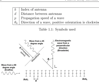
A schematic representation of a phased array antenna system is shown in gure 1.1. This systems shows a standard setup of a possible array. The array is placed in the horizontal plane with antenna elements from west (left) to east (right). A signal coming from the north direction is coming perpendicular to the array. A signal from the west direction is coming parallel to the array, the array is build of equally spaced antennas. All signals drawn in the gure travel along the horizontal plane.
The signal arriving at the kth antenna has a delay of
(d/p)sin(−θ0)×k (1.1)
seconds relatively to the rst antenna. The symbols used in this equation are shown in table 1.1, these symbols will be used throughout this document. The angle θ0 is measured relatively to the perpendicular of the array.
1.2 Processing
2 Phased array antenna processing
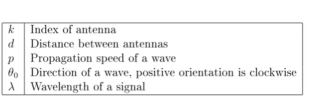
k Index of antenna
d Distance between antennas p Propagation speed of a wave
θ0 Direction of a wave, positive orientation is clockwise
Table 1.1: Symbols used
Figure 1.1: Schematic representation of a line antenna array, top view
direction. By adapting parameters in the beam forming process, the direction can be steered. The processed signals of the antennas are added together to form this beam. This processing can be performed in dierent ways.
First a decision is made in which domain this processing is done. Signal processing can be done in both the analog and the digital domain. Analog signal processing requires devices such as phase shifters or delay lines for beam forming. A disadvantage of these devices is that they introduce signal loss, which results in less signal power and, after amplication, a lower signal to noise ratio. This signal loss gets worse when more devices, such as phase shifters, are used or many beams are created. Processing in the digital do-main gives a number of advantages. After the signal is sampled and digitized at the analog to digital converters, no signal loss will occur. Multiple beams can be made without power loss. Digital processing gives exibility in the steering direction. And the steering direction can be changed quickly when software processors are used.
1.3 Problem description 3
signals these signals are converted by analog-to-digital-converters (ADC). The frequency of conversion is called sampling frequency (Fs).
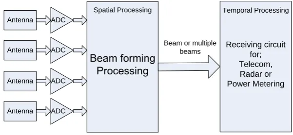
A schematic representation of a beam forming system with the location of the processing algorithms is shown in gure 1.2. Dierent strategies for processing are searched and are explained in the chapter 4.
Spatial Processing
Figure 1.2: Total system with processing stages
1.3 Problem description
The assignment of this thesis is about the research of current techniques in beam forming and to build a validation platform for beam forming with the use of recongurable hardware. The recongurable hardware is the Mon-tium. It is expected that this processor will be able to eciently process phased array signals. Digital Beam Forming is very calculation intensive and the Montium is a energy ecient processor. A beam former system which implements this processor rather than a general purpose processor or FPGA will be more energy ecient.
Chapter 2
Literature
2.1 Introduction to Radar Systems
The book Introduction to Radar Systems [1] explains the basics of radar and radar processing. It covers radar systems and dierent technologies to design radar systems. The book also covers noise and clutter (weather and environmental distortion), which can be observed in practical radars. Chapter 9 explains possible antennas that can be used to create a radar system. In this chapter the application of beam forming is explained and how this can be done in an analog and a digital manner.
In this chapter also a discussion about Baseband and IF Digitizing is made. When IF Digitizing is used with in-phase and quadrature signals, conversion with two analog to digital converters (ADC) can be done with a minimum sampling rate of 1.4 times the signal (half-power) bandwidth. It was stated by [11] that with direct digitizing of the baseband signal with only one ADC channel the minimum sampling rate becomes 5.4 times the signal bandwidth. The sampling rate has to be higher than the theoretical Nyquist rate of two times the signal bandwidth for avoiding distortion of the signal spectrum caused by folding.
2.2 Array and Phased Array Antenna Basics
6 Literature
around -13 dB of the main beam for a phased array. The remaining chapters are about dierent phased array topologies and discusses their designs and performance. Also how antenna measurements can be performed is written. This book focuses highly on electrical engineering of antennas.
2.3 Smart Antennas
Chapter 3
Related work
3.1 Radio Astronomy Receivers
In radio astronomy, the universe is studied about solar systems and stars. One of the methods for observation is to receive electromagnetic waves send out by stars. The classical approach for this is to use large dish antennas. However, in the search of higher reception quality now also the use of phased array antennas is studied.
One example of such an antenna is developed by ASTRON, in [6] a phased array antenna telescope demonstrator is described. This demonstrator con-sists of 256 elements and is used for evaluation of the phased array antenna concept for astronomical research. In this paper a brief description of the thousand element array and the square kilometer array concept is given as well as results from the demonstrator.
The concept consists of tiles with 64 antennas. These tiles rst perform analog RF beam forming to create two beams. From there, the result is down converted, digitized and transported over glasber to a digital beam former. This digital beam former is able to sum dierent beams and the result is passed through a Digital Signal Processing (DSP) board. This DSP board performs the calculations needed for evaluations of the radio astronomy signals.
This design represents certain aspects of the problems encountered in Digital Beam Forming (DBF). The digitalization is done with a sample rate of 40 MHz. ASTRON has chosen to equip the DBF with FPGA's. Currently this is a method which is widely used for digital beam forming. [8, 9]
8 Related work
3.2 Optical Beam Forming Networks
At the research group Telecommunication Engineering of this faculty a beam forming network is developed with the use of laser optics. This is called an optical beam forming network (OBFN) [10], the system uses optical ring resonators (ORRs) to establish a continuously tunable time delay. The OBFN is created by using a binary tree-based hierarchy of ORRs and by using optical combining/splitting circuitry.
In theory this system can beamform broadband signals because it uses time delay rather than a phase shift. Such an approach can be useful in a number of applications. An actual design of an OBFN is designed with one input and 8 outputs, measurements are performed on a stage of 4 outputs. The design is tuned such that three linearly increasing delays are obtained over 1.5 GHz bandwidth. The largest delay value is approximately 0.5 ns (corresponding to 15 cm of physical distance in air) and a delay ripple of approximately 20 ps (6 mm).
3.3 Mobile Satellite Reception
For the reception of satellite signals often dish antennas are used. These antennas need to be setup precisely because of the high angular reception. When pointed directly to a satellite, a signal is received which can be used for television or communication. The setup is xed and can therefore not be moved, in a mobile situation such high angular reception could be performed with the use of a phased array antenna.
In Digital Beam Forming Antenna System for Mobile Communications [8], which is written in combination with [13], the feasibility of a Digital Beam Former (DBF) for satellite communication is evaluated. A DSP system is built for the evaluation of reception capabilities of this system. As a reference a Japanese test satellite is used for the reception of an unmodulated signal. The system is built up of 16 antennas and with 128 KHz sampling ADC. Processing is done with FPGA's. These FPGA's are used to implement a DBF using Fast Fourier Transforms. For the creation of quadrature signals a digital local oscillator is used in combination of a FIR lter.
3.4 Base Station Communication 9
3.4 Base Station Communication
In the last decade mobile communication has rapidly grown. For mobile communication parts of the spectrum are used to transmit and receive signals. Because this is getting used more intensively the spectrum occupation grows, one solution can be to separate transmission signals in space.
A possible implementation of such a solution is written in [7]. It han-dles mobile base communications for ground stations. A cyclic phased array antenna is used with patch antennas and an analog beam former network is used for feeding this array. The goal of the project is to increase coverage radius and reduce transmit power of a base station, the cyclic phased array antenna has a high gain which is steerable and can be used to accomplish these goals.
In a satellite communication system separation in space is introduced in [9], supported by ESA/ESTEC in Noordwijk, the Netherlands. The commu-nication system deals with the problems at the satellite site. A phased array antenna is mounted on a satellite and uses a system for multiple access from the earth. The proposed system features a frequency division multiplexer demultiplexer with a beam forming network.
This system has high specications, the resources used are limited as only one ASIC is used to handle multiple channels. The proposed solution is a highly integrated system of lters and Fourier transforms.
3.5 The Montium, a coarse-grained
recong-urable processor
The Montium is a processor developed at the University of Twente as part of the Ph.D. thesis of P. Heysters [4]. The Montium can be used as a part of a system on chip. In such a chip, several processors communicate and exchange data with each other. The Montium is therefore also referred to as tile processor. Currently the development of this chip and development tools is handled by Recore Systems [5] which sells this Montium as an Intellectual Property Core (IP core).
Chapter 4
Methods for beam forming
The beam forming explained in Chapter 1 is studied in detail and reference designs to process signals from phased array antennas. The number of digital implementations is limited. In this chapter we restrict to; time delay, phase shift and Fast Fourier Transform.
4.1 Time delay
One method to create a beam is to compensate for the time delay experienced by the dierent antennas. This time delay can be compensated relatively to the antenna which receives the signal as last one, a reference antenna. The antenna rst receiving the signal buers this signal until the wavefront reaches the last antenna. The time delay (τk) in seconds experienced by the
antenna for the kth antenna is (equation 1.1):
τk = (d/p)sin(−θ0)×k (4.1)
k Index of antenna
d Distance between antennas p Propagation speed of a wave
θ0 Direction of a wave, positive orientation is clockwise
λ Wavelength of a signal
Table 4.1: Symbols used
12 Methods for beam forming
individually. The outputs of the individual delay lines are summed together and form one beam. The resolution of this method is dependent on the smallest time delay, which can be realized by the delay lines.
In the case the signal is compensated relative to an antenna which does not receive the signal last, this −τk will be negative and a negative delay
line should be constructed. Such a delay line should contain future signals and is not feasible. A way to solve this is to add a constant delay equal for all the antennas, which eectively compensates relative to the last receiving antenna again.
Time delay works for wideband signals built up of arbitrary frequencies, not only narrowband signals. This is due to the fact that it compensates for the real experienced dierences between antennas. This makes the approach a good solution for processing audio signals, because these signals are typi-cally wideband. The response of beam forming methods also depends on the spacing (d) between antennas. In [2] a limit is calculated for the distance d.
It is required that d
λ ≤1 should be satised otherwise grating lobes appear.
In this formula,λis the wavelength of the signal. Grating lobes are duplicate
beams with the same sensitivity as the main beam, but from unwanted di-rections. The spacingdis takenλ/2, this spacing generates the most number
of nulls without creating ambiguity in the main beam.
As explained in the previous paragraph, beam forming responses are de-pendent on the locations of the antennas with respect to the wavelength of the signal. Compensating time delay is said to work for arbitrary frequencies, however, the virtual distance between antennas vary. This is a result from changing frequencies and therefore changing wavelengths. The result is that the beam width of the main beam depends on the frequency.
4.2 Phase shift
A signal which has only a small bandwidth, can be simplied by a single sinusoidal signal. This is called the the narrowband assumption. For a sinusoidal signal, a momentarily value can be recreated by shifting this signal with the right part of the periodic length. Such part of a period is called phase. Thus, by changing the phase of a signal it can be shifted in time.
To calculate this phase shift a few values are needed, the distance that needs to be compensated and the wavelength of the signal. The wavelength of the signal is on its turn dependent on the frequency of its signal and the propagation speed of the wave in its medium. The wavelength (λ) is
4.2 Phase shift 13
will be
λ = p
f (4.2)
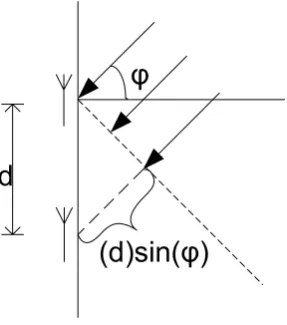
In gure 4.1 an example phased array is shown. The antennas are sepa-rated dmeters. A wavefront which is traveling perpendicular to the array is
received at all antennas at the same time.
φ
(d)sin(
φ
)
d
Figure 4.1: Schematic representation of two array elements with a wavefront
When a wavefront is coming from an angle like in the gure, the wave-front and the array form a triangle. At the time the wavewave-front reaches the upper antenna, the distance from the wavefront to the lower antenna can be calculated with a goniometric calculation:
∆x=d×sin(ϕ)
The signal at the lower antenna needs to be shifted forward in time. This can be done by giving this signal a positive phase shift. This phase shift is equal to 2π ×∆x/λ. This phase shift is calculated for a larger array in a
linearly fashion for regularly spaced antennas. The distance that needs to be compensated grows linear for thekth antenna, the phase shift (ψ
k) in radials
also grows linear. For the total array it becomes:
ψk = 2π(d/λ)sin(θ0)×k (4.3)
14 Methods for beam forming
k Index of antenna
d Distance between antennas p Propagation speed of a wave
θ0 Direction of a wave, positive orientation is clockwise
λ Wavelength of a wave in its medium τk Time delay
ψk Phase shift
Fs Sampling frequency
Table 4.2: Updated symbol list
4.3 Butler or FFT transform
The Butler Beam-Forming Array is explained in [1] and can be used to form N beams out of an N-element antenna array. The Butler matrix uses special electronic devices named hybrid junctions and static phase shifters. This Butler matrix is the analog version of the Fast Fourier Transformation (FFT). When the signals of the antennas are digitized, they can be fed into the FFT. A great advantage of this method is that after this processing, the output consists of multiple beams pointed in dierent directions. Specically this transformation creates as many beams as input antennas fed into the Fourier transformation.
The Fast Fourier Transform was originally designed for transforming a time signal into a frequency response. The signal induced on an antenna array is also in the form of dierent frequencies, signals from dierent directions generate dierent frequencies when observed in the spatial domain. Let an antenna array consist of elements positioned λ/2 from each other. In case
the signal is induced from the direction perpendicular to the antenna array it induces equal voltage over the antennas, because the signal is the same at each antenna at every moment in time. When a signal is induced in an small angle over the array, the signal is slightly dierent at each antenna. This results in an ac voltage in the spatial domain. Let the signal be induced in the direction of the array (end-re), the signal diersλ/2between all antenna
elements, which results in the highest frequency possible. By using an FFT these frequencies which represent deerent angles can be separated and used as dierent beams.
4.3 Butler or FFT transform 15
−80 −60 −40 −20 0 20 40 60 80 −30
−25 −20 −15 −10 −5 0
Response of beamforming 16 antennas, d=150m λ=300m
Beamforming angle relative to normal
Amplitude response (dB)
Figure 4.2: Response of phased array processing using t processing, angle of -90 to 90 degrees in 16 steps
−50 0 50
−60 −50 −40 −30 −20 −10 0
Response of beam forming d=0.5λ
Angle relative to normal (degrees)
Amplitude response (dB)
16 Methods for beam forming
4.4 Antenna multiplicity
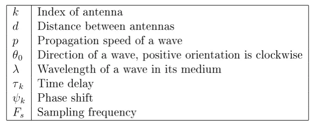
The directional sensitivity of the beams created by beam forming are depen-dent of the number of antennas used. By using more antennas the antennas receive more information about the direction of the signal, which results in a higher angular resolution. In gure 4.3 the response of three dierent phased array antenna systems is drawn. One system with four antennas, which has the lowest angular resolution. One with 16 antennas, the intermediate and one with 64 antennas, which has the best relative angular resolution. The -3dB bandwidth is 2 degrees.
4.5 Beam width and side lobes
The main beam width and side lobes are dependent on each other. By using amplitude weighting on the individual antenna elements the shape of the main beam and the side-lobes can be altered. In [2] it is stated that by using a binomial distribution over the elements, the side lobes can be suppressed all together. However, the resulting main lobe then gets wider. For phase shifting with complex multiplications this can be applied to all input signals. The shape of the main beam can be tuned. In case multiple beams are created with individual sets of coecients, all these beams can be tuned individually. What is more interesting is that there is a trade-o between the width of the beam and the amount of suppression of the side lobs, depending on the used weights. The binomial distribution is one extreme of this. This is because of the uncertainly principle.
In a FFT approach complex multiplications are re-used. The consequence is that all beams get the same shape. Individual beam shaping in a FFT approach is not possible.
The beam width and side lobes also depend on the distribution of the antennas. In this document equal distance between antennas is assumed. Other congurations are possible to change the sensitivity of the array and to change beam width, however, this will not be taken into consideration in this thesis.
4.6 Advanced beam steering
4.6 Advanced beam steering 17
steering algorithm is optimal with respect to an optimization criterium. An example criterium could be to produce the highest possible signal to noise ratio. Many of these algorithms work with some sort of digital feedback lter, in which case the optimal beam steerer dynamically changes the coecients of the beam former.
Chapter 5
Beam forming algorithms
The previous chapter explained how phased array antenna signals can be processed in theory. In this chapter, suitable digital algorithms will be intro-duced to process these signals on a computer: Time Delay, Complex Multi-plication and Fast Fourier Transform.
5.1 Time delay
This method uses processing on the individual signals to create one beam at a time. Through multiple processing stages, multiple beams can be created. The time dierence introduced by the dierent locations of the antennas is compensated with a time shift. After the compensated time shift the signal can be summed and a beam is created.
5.1.1 Algorithm
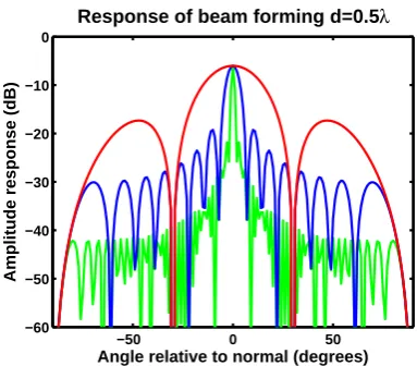
The approach is to control the delay signals from individual antenna, which can be done with the use of a buer. The samples are rst stored in a buer and, when time expires, the samples can be read again. The buer is lled with a rate equal to the sampling frequency (Fs) and the buer is as long as
equation 4.1 prescribes. Afterwards the samples are summed.
The buer is lled at a xed rate every1/Fsseconds and the delay length
can only be made an integer multiple of this time. To be able to construct all dierentτkvalues as needed, one could try to increase the sampling frequency
20 Beam forming algorithms
5.1.2 Interpolating
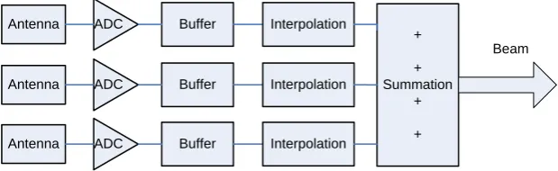
The resolution of the delay elements depends on the sampling frequency. For a typical beam forming application, it should be possible to point in randomly selected directions. This can result in delays which are not an integer multiple of the time steps of the sampling frequency. A naive solution is to round all delays of the antennas to the nearest integer. However this will introduce an error and will have consequences for precision. The response of such a solution is shown in gure 5.4(b).
A solution could be to combine a time delay buer with interpolation. In this case, interpolation is used for time delays which are not an integer multiple of the sampling time. Interpolation is a technique to calculate values between sample moments. Higher order interpolation can be used to make the interpolation result better. Higher order interpolation uses more sample moments and results in better approximation of the original signal.
Antenna ADC
Figure 5.1: Schematic of signal ow with time delay using buers and inter-polating
The Shannon sampling theorem prescribes the minimum sampling fre-quency needed for signal reconstruction. This should be at least two times the signal bandwidth. For reconstruction the Whittaker-Shannon interpola-tion formula can be used;
x(t) =
This interpolation formula uses a sinc function, which is shown in red in
5.1 Time delay 21
response of an approximation is shown in gure 5.3 for a rst, a 32th and a 64th order approximation. As a reference the ideal frequency response of the
sinc function is shown in red.
−10 −5 0 5 10
−0.4 −0.2 0 0.2 0.4 0.6 0.8 1
Interpolation
samples
factor
Figure 5.2: Impuls response of linear interpolation (blue) and an ideal sinc(x) interpolation (red)
0 0.5 1 1.5 2 2.5 3
−50 −40 −30 −20 −10 0 10
Interpolation response
normalized frequency
H() [dB]
Figure 5.3: Frequency response of linear interpolation (blue), an ideal sinc(x) interpolation (red), a 32th order approximation (green) and a 64th order
22 Beam forming algorithms
5.1.3 Computational complexity
The time delay method consist of two elements, the buer element and the interpolation element. The buer element uses memory to store samples. The interpolation element uses only multiplication with a constant and additions, hence no memory is needed. The maximum memory depth required for buering occurs when the signal travels along side the phased array, the rst antenna encountered must store its samples until the wavefront reaches the last antenna. When the antennas are spaceddmeters apart, the propagation
speed is pand the sampling frequency Fs the maximum memory depth is
d
pFs (5.1)
samples. For one antenna, as the direction of the signal can be altered, each outer most antenna will need such a buer depth. Reaching the middle of the array the needed buer is half of that.
The number of multiplications required for interpolation is one multipli-cation for each interpolation coecient. For N antennas and B beams this
formula is;
(1·Order+ 1)·N ·B ·Fs (5.2)
multiply accumulate instructions per second.
5.1.4 Simulation
A Time Delay algorithm is simulated in MATLAB implementing an
algo-rithm which rounds sample times and an algoalgo-rithm which interpolates the samples with a rst order interpolation. The simulation projects a beam on the phased array antenna as if it is received from a 45 degree direction of arrival. The parameters of this algorithm are varied with time delaysτk,
which are calculated with equation 4.1 to scan from -90 to 90 degrees. MAT-LAB simulates sinusoidal wave signals from the antennas. These signals are
buered and the simulation employs rounded time delays and interpolated time delays. Afterwards the signals are summed and the power of this beam is calculated. This calculated power is plot against dierent beam steering coecients. The simulated received signal on the antennas is from a constant direction. In gure 5.4(b) the response without interpolation and in gure 5.4(c) the response with rst order interpolation is shown.
5.1 Time delay 23
Response of beamforming 16 antennas, d=0.5λ fs=20f
Angle relative to normal (degrees)
Amplitude response (dB)
(a) Ideal response, Linear interpolation, Fs
= 20Fsignal
Response of beamforming 16 antennas, d=0.5λ fs=2f
Angle relative to normal (degrees)
Amplitude response (dB)
Response of beamforming 16 antennas, d=0.5λ fs=2f
Angle relative to normal (degrees)
Amplitude response (dB)
(c) Linear interpolation,Fs= 2Fsignal
24 Beam forming algorithms
5.2 Complex multiplication
The complex multiplication method uses processing on the individual signals of multiple antennas to create one beam at a time. The phase shift introduced by the spacing of the antennas is compensated with a complex multiplication. After this multiplication all signals from one direction are in phase with each other and a cumulative signal can be made by adding all signals together. This is under the assumption that narrowband signals are processed.
5.2.1 Quadrature and in-phase signals
For the algorithm to work, every sample in the time domain needs to be manipulated in phase. The signal gathered by the ADC consists of a real signal, but does not yet contain phase information in its samples. This can be seen when a momentarily value is studied. When, for example, a real value from the ADC is sampled, its value could be `2'. With this information it is not possible to know what the phase of a sinusiodional is.
One way to represent complex signals which can include phase informa-tion is using quadrature signals. Together with a real signal, an extra signal is created which lags 90 degrees in phase. For example, when together with the real `2' an 90 degrees o `1' signal is present, they represent a phase of
tan
degrees. So to store phase information in samples a secondary signal is needed. This signal is called a quadrature signal. In the analog domain, this signal can be created with the use of a local oscillator (LO); at one side the direct LO signal and at the other side a 90 degrees shifted LO signal. These signals are multiplied with the received signal and because of this they are called in-phase and quadrature signals.
5.2.2 Hilbert transformer
A Hilbert transformer can also be used to construct a quadrature signal with the in-phase signal as input. This is done by shifting positive frequencies -90 degrees and negative frequencies 90 degrees. In [12] a transformation is made from the frequency domain to the time domain. The formula which describes the Fourier relation is;
5.2 Complex multiplication 25
The right part of equation 5.3 represent the Hilbert function in the fre-quency domain. The positive frequencies get a -90 degrees shift through the multiplication in the frequency domain with−j, while the negative
frequen-cies get a multiplication with j in the frequency domain.
The Fourier transform of the Hilbert function consists of imaginary values only. In the time domain, the function 1/πtcan be approximated by a set of
sine waves. By using this time domain function of the Hilbert transformer, it is possible to implement the Hilbert function using a Finite Impuls Response (FIR) lter. Filter coecients can be calculated byMATLABand an example
of an impulse response is shown in gure 5.5.
0 10 20 30 40 50 60
Figure 5.5: Impulse response of a Hilbert lter
26 Beam forming algorithms
An example Hilbert FIR lter is designed withMATLAB. It is a16th order
lter which has 17 coecients. The frequency response is shown in gure 5.6.
0 0.1 0.2 0.3 0.4 0.5 0.6 0.7 0.8 0.9 1
−6 −5 −4 −3 −2 −1 0 1 2
Hilbert frequency response
Normalized Frequency (xπ rad/sample)
Magnitude (dB)
Figure 5.6: Frequency response of a Hilbert FIR lter
As seen in gure 5.5, half of the coecients are zeros. In an optimal implementation, multiplications where these zero-coecients are involved can be skipped as they do not inuence the result, resulting in only half the multiply accumulate (MAC) instructions as normal. The example16th order
lter can with some added control be processed with 8 MAC instructions. The signal which travels through the Hilbert lter experiences a group delay of half the lter length. This delay is introduced in FIR lter design, the FIR lter applies a convolution with the coecients. The coecients represent the impulse response of a desired frequency response. Because this impulse response is not causal, this impulse response is shifted in time over half the lter length.
The delay must also be given to the in-phase signal. To accomplish this, a group delay block is introduced in the signal path of the in phase signal.
5.2.3 Algorithm
5.2 Complex multiplication 27
one and a phase which is based on formula 4.3.
ρk = 1·ej·ψk (5.4)
With the complex exponent this results in a complex vector. The signal needs to be multiplied with this constant complex vector (ρk). A complex value
is a pair of real values. For a complex multiplication four multiplications of real values are processed.
A schematic overview of the total Hilbert lter + Complex Multiplication system is given in gure 5.7.
Beam
Q
I
Antenna ADC
Grp delay
Hilbert Q
I
mac mac
mac mac
Figure 5.7: Schematic signal ow with complex multiplication
5.2.4 Computational complexity
The previous description consists of two steps. First, for each antenna a Hilbert process is started to create a complex signal, second, for each beam the complex multiplication has to be performed. The rst step uses the FIR lter order (H) divided by 2 MAC instructions for each sample moment.
This is done for allN antennas. The second step uses four MAC instructions
for all N antennas, for eachB beams and for each sample moment (Fs). In
formula form this becomes
(H/2·N +B ·N ·4)×Fs (5.5)
28 Beam forming algorithms
5.3 Fast Fourier transform processing
With the use of a Fast Fourier Transform (FFT) phased array signals can be processed in a single algorithm to multiple beams. The FFT therefore re-uses intermediate calculations. It is more ecient than the phase shift method.
5.3.1 Quadrature and in-phase signals
The FFT processing also requires a complex signal. This is because the FFT is an optimisation of the complex number multiplication and requires phase information. If this is not done, a FFT can not separate the negative and positive frequencies. These negative and positive frequencies form the left and the right intercept angles of the phased array antenna.
5.3.2 A spatial Fast Fourier Transform as beam former
The FFT processes all the antenna signal sampled at a specic point in time. This method createsN beams from an array ofN antennas. The FFT
algorithm computes the discrete Fourier transform (DFT) of a signal (x[n]),
the equation of the DFT is:
X[k] = N−1 X
n=0
WNnkx[n] (5.6)
where
WNnk =e−j2πN·nk (5.7)
A schematic representation of the algorithm is presented in gure 5.8.
5.3.3 Computational complexity
In the case of N antennas and a sampling frequency Fs, to create the same
number of beams as antennas the FFT algorithm needs [4]
4·(N/2)·log2(N)·Fs (5.8)
5.4 Comparison of algorithms 29
Antenna ADC
I and Q pair
Beams
Grp delay Hilbert Q
I
Antenna ADC
Grp delay Hilbert Q
I
Spatial Fast Fourier
Transform
I and Q pair
Figure 5.8: Schematic signal ow with FFT processing
5.4 Comparison of algorithms
The algorithms explained in this chapter use dierent amount of resources from a processor. To give an impression about the relative computational capacity needed by the three algorithms, a gure is made. Figure 5.9 shows such a comparison. On the vertical axis the number of multiply accumulate instructions needed on each sampling moment is given. On the horizontal axis the number of input antennas is given. The methods of complex multi-plications and FFT uses a Hilbert pre-lter of 16th order.
An example, the FFT approach with 128 antennas takes about4·103·F
s
MAC instructions. This means that 4000 MAC instructions have to be
30 Beam forming algorithms
2 4 8 16 32 64 128 256 512 1024 2048 4096 100
101 102 103 104 105 106 107 108
Antennas
Multiplications x F
s
Computational load
True Time delay (linear interpolating) Complex multiplications + Hilbert filter Fourier Transform + Hilbert filter
Complex multiplications + Hilbert filter (N−Beams)
Chapter 6
Testplatform design
6.1 Introduction
The test platform is built on a development board of Xilinx [17]. This de-velopment board has a FPGA, a number of input, output peripherals and is equipped with hardware to build an embedded system. The FPGA is a Virtex II Pro, this FPGA has next to the standard FPGA slices also block RAMs, multiplier slices and two PowerPCs. A PowerPC is a general pur-pose processor. For a beam forming testplatform audio signals are taken to be evaluated. Audio signal can be made with a predetermined spectrum and with the use of microphones these signals can be received. The received analog signal is converted with analog to digital converts (ADC) to a digital signal. These digital signals lines are connected to the FPGA.
6.2 Development
Developing a system on the development board can be done with the use of the Xilinx Platform Studio (XPS) software [18]. The studio delivers support for a hardware project with multiple software projects. The project is usually started with a base system builder wizards [16] which gives a foundation for the rest of the project. The wizard needs a User Peripheral Repository which gives a description of the development board. The output of the wizard consists of a complete (compilable) project which can be downloaded for evaluation.
32 Testplatform design
Impact
Impact is a tool that can be used to program the development platform. This tool support all methods for conguring and handles the le translation between dierent formats. The board can be congured in a number of ways, for example, it can directly be programmed through the embedded platform USB connection, it can be congured with the use of the onboard ash PROM or it can be congured with the use of a Compact Flash card. Downloading software is done using Boundary Scan (IEEE 1149.1 /IEEE 1532).
Integrated Software Environment
The Integrated Software Environment (ISE) is the environment used by XPS to synthesize hardware designs. The hardware designs (for example VHDL descriptions) are managed by XPS and are compiled with this pro-gram. The input is a hardware description language and the output are net lists and place-and-route information.
6.3 System design
The system design is shown in gure 6.1, main parts are the Montium, the ADC interface and the PowerPC. The Montium TP is synthesized from its VHDL source and congured into FPGA space. For interfacing with the ADCs an interface is build in VHDL, this interface is described in appendix A. This VHDL interface is synthesized and congured into the FPGA next to the Montium.
6.3 System design 33
34 Testplatform design
6.4 Beam former data ow
The testplatform design uses audio signals as source and applies beam form-ing on these audio signals. These input signals are made with the use of 8 microphones and are converted with 8 ADCs. The ADCs are embedded on an ADC-module, a single module consists of two ADC from National Semiconductors type ADCS7476 [19]. The modules digital signal lines are connected to the development board and are connected to FPGA pins. From here the processing is done on the FPGA chip, the data ow of the dierent processing stages are shown in gure 6.2 and 6.3 for the dierent methods.
The data ows are annotated with processing algorithms (above the blocks) and mapping information (beneath the blocks). The blocks are given a functional description.
Time Delay or Phase Shift algorithm
Figure 6.2: Data ow of a single stage (Time Delay or Phase Shift) process
AD
Chapter 7
Mapping beam forming
algorithms to recongurable
hardware
7.1 Introduction
This chapter will show how the previously explained algorithms have been implemented on the Montium processor. First the Time Delay algorithm implementation is explained. Then the implementation of a Hilbert lter together with the Complex Multiplication. Finally it is shown how the results of the Hilbert lter can be used for the Fast Fourier Transform.
The algorithm implementations are made for a system with 8 input an-tennas/channels.
7.2 Time Delay
The Time Delay algorithm consists of buering, interpolation and summa-tion. The following implementation is for a system which consists of 8 an-tennas, also called channels in this text. A trade o is made which combines interpolation with a feasible amount of processor power. The implementation made is an algorithm which uses a linear interpolation. Linear interpolation stores two samples in the registers and gives weights corresponding linearly to the distance of the required time and the sampling time. The resulting frequency response of this implementation is shown in gure 5.3.
The Montium receives samples, one sample Xk,i for each channel (k) for
each sampling time (i) and outputs a single value for each sampling time.
36 Mapping beam forming algorithms to recongurable hardware
In the following sections these steps are explained. The steps are for a single channel. The Montium is a parallel machine and the steps can be performed for 5 channels in parallel; each Processing Part handles one channel at a time.
Buering
Buering is done with the use of a cyclic buer. This buer uses the memories of the Montium. Each channel is given its own memory, because the Montium is equipped with 10 memories it can serve 10 channels. A cyclic buer is formed by incrementing the pointers with a modulo function. Two pointers are introduced, one writepointer which stores the location where the buer is lled and one readpointer where the buer is read.
The pointers are stored in registers of the ALU. When a sample is calcu-lated these pointer are incremented. In each iteration, incoming samples (X)
are stored at the position of the writepointer and a sample at the readpointer is forwarded to a register (R).
Interpolation
The sample stored in the register is multiplied with an interpolation coe-cient and stored in a register, mathematical:
A=R[n]·Cinterpolation[1]
In the CDL1code the interpolation coecientsC
interpolation[1]andCinterpolation[2]
are called FIRST and SECOND, respectively. In CDL code the interpolation is: // Multiply NEWREGm1 (c1) sample with FIRSTm1 coeff. (b2) alu p3c1 fmul p3b2 sadd p3es -> p3ws
In the next clock cycle the previous sample X[n−1] =R[n−1] is used
and multiplied with the second interpolation coecient. In the same clock cycle this value is added to the previously calculated value A:
I =R[n−1]·Cinterpolation[2] +A
clock
// Multiply OLDREGm1 (b1) sample with SECONDm1 coeff. (c2) alu p3b1 fmul p3c2 sadd p3es -> p3ws
Now an interpolated sample I is calculated for this channel. This sample
(Ik,i) is used for summation.
7.2 Time Delay 37
Figure 7.1: Memory and ALU register mapping
Summation
Summation is done by adding all samples Ik,i from the dierent processing
parts together to form the resulting output sample Yi. Summation is done
with the use of the east-west connections of the ALUs. The summation of dif-ferent processing parts is done in parallel with interpolation. The calculated valueAbecomes then a cumulative value for 4 channels and is calculated by
addingIk,i for k = 0 to3. In the second stage (channels 4 to 7) this value is
added with Ik,i for k= 4 to7.
In the rst stage;
Yi =
3 X
k=0
Yk,i
and in the second stage;
Yi =
7 X
k=4
Yk,i+Yi
38 Mapping beam forming algorithms to recongurable hardware
Clock cycles
The algorithm on the Montium uses 10 cycles for one output sample2. This
can only be seen in the source code, provided in appendix B. For the mul-tiplication 4 cycles are used, 4 more for pointer updating and 2 for input, output communications.
2The Montium processor is a complex processor which can do a lot in parallel. The
7.3 Hilbert ltering 39
7.3 Hilbert ltering
The complex multiplication implementation is made with a preprocessor which lters the incoming data. This lter is a Hilbert FIR lter which generates information about the phase of the signal received. This Hilbert lter is implemented as a FIR lter in an optimized way. And is capable to process multiple channels in parallel.
The Montium receives as before a sample (Xk,i) for each channel (k)
every sampling time (i). These samples are ltered and the Hilbert stage
will output two values: the ltered quadrature (Im) value and the in-phase
value (Re).
The number of samples which have to be calculated is preferred to be a power of 2. This results in an ecient mapping on the Montium AGUs. The implemented Hilbert lter is a16thorder lter. The lter coecients (C
j) are
calculated byMATLAB. This results in 17 coecients of which 9 (rounded to the nearest 16 bits number representation) are zero, 8 coecients remain to be calculated by the processor. The frequency response of a 16th order lter
is given in gure 5.6.
Buering
First the Hilbert lter buers the incoming samples Xi in a cyclic buer
(which is a modied version of [14]). The algorithm is made for 8 input channels in the spatial domain which are stored in the rst 8 memories of the Montium. These buers are split in two sections of which the odd and even temporal index (i) ofXk,iare separated. In the current implementation,
these odd and even samples are split up in two partitions of the memory, each 8 samples long.
Filtering
The Hilbert coecients (Cj) are stored in an additional memory, memory 9,
of the processor. This memory is used by all processing parts to multiply the incoming data with.
Imk,i =Xk,(i−j)·Cj+Imk,i for j = 1 till 8
Group delay
40 Mapping beam forming algorithms to recongurable hardware
back.
Rek,i=Xk,(i−O/2) for O = Order of lter
Clock cycles
The algorithm on the Montium uses 21 cycles for one sampling time. For the multiplication 2·8 cycles are used, 2 for overhead of pointers and 3 for
input, output communications.
7.4 Complex Multiplication
The output of the Hilbert lter is stored in registers. The complex multi-plication (CM) continues processing with these values. It should multiply the complex signal pairs (Im and Re) with complex coecients. It does this
only to the extend that it calculates the resulting real values (Re). The
re-sult of the imaginary value (Im) is not calculated. This is done because the
post-processing stage, power calculation, does not require a complex signal.
Clock cycles
The algorithm on the Montium uses 7 cycles for one sampling time. For the multiplication of 8 complex signal pairs with 8 coecients 5 cycles are used, 1 for overhead and 1 for input, output communications.
A complex signal pair multiplication requires 4 clock cycles on one pro-cessing part, now only 2 clock cycles are used. Because one propro-cessing part handles two channels, the processing parts need 4 clock cycles. For the nal summation of all 8 signals the accumulated results of the processing parts are added in a nal summation clock cycle.
7.4.1 Results
The test setup is made with the development board (chapter 6) and the Montium conguration for CM.
The test is made with a signal generator, generating a sinus with a RMS value of 126mV (gure 7.3(b)). This signal is split in 8 and fed through
the inputs of the ADC and is beam formed in the Montium processor. The PowerPC calculates the power received. This test signal should result in a power of
20∗log(126mV ×8) = 60.069dBmV
7.5 Fast Fourier Transform 41
Figure 7.2: Memory and ALU register mapping
7.5 Fast Fourier Transform
The Fast Fourier Transform (FFT) implementation uses the results of the Hilbert FIR lter as input data. The stream of Rek,i and Imk,i (complex)
values of the Hilbert lter are rst stored in a temporal buer in the PowerPC (see section 6.4). When the buer is lled, these complex values are streamed toward the FFT algorithm.
Implementation
The implementation of the Fast Fourier Transform is supplied by [5] as a binary conguration le. The implementation calculates the FFT of the input samples and does reordering of the output samples afterward. Reordering is a technique that enables a logical output order of the samples of the FFT. The core of a FFT routine delivers its output samples in a bit-reversed order.
The implementation uses 29 clock cycles in the Montium simulator (see section C.4). The implementation uses;
N
2 + 2
42 Mapping beam forming algorithms to recongurable hardware
(a) Output spectrum of test setup,
hy-perterminal output (b) Input signal for test setup, generatedwith a function generator
−10040 −50 0 50 100
Response from Beam Former 50
(c) Output spectrum of feed with signal generator (other setup), Matlab output
−100 −50 0 50 100
Response from Beam Former 100
(d) Output spectrum of an audio source at a distance of around 2 meters, Matlab output
Figure 7.3: Response of an beam former implementation with Complex Mul-tiplications
clock cycles for the FFT algorithm. In this case it should use 6∗3 = 18
cycles, the additional cycles are used for reordering.
7.6 Mapping results
A comparison of the dierent implementations is given. Table 7.1 shows the clock cycles minimum needed for calculating all multiply accumulate instructions. These are based on the formulas in chapter 5 and are the ideal values. The table shows the clock cycles needed in the implementations as given in this chapter.
7.6 Mapping results 43
this results in the most ecient mapping and a fair comparison of ideal and implemented values are possible then.
Algorithm Ideal Implemented Remarks
Time Delay 4 10 1st order interpolation, 1 beam
Phase Shift 20 29 Re/in-phase output only, 1 beam
Phase Shift 24 33 Complex output, cycle usage is an estimation Hilbert FIR 16 21
FFT 12 29 Complex output, N beams,
Chapter 8
Applications
A beam former can be designed for dierent application purposes. For these dierent purposes, the design parameters diers considerably. First an overview of dierent Montium implementations with their operation speed will be given. Then a number of possible scenarios are given in which beam forming can be applied.
8.1 Montium processing throughput
The current Montium implementation on the BCVP1 reaches clock speeds
of around 6 MHz. For some applications mentioned in this chapter this is not sucient high. In the Annabelle2 chip clock speed of 25 MHz (worst
case) to 100 MHz (best case) are reached. For this chip a 100 MHz Montium clock speed will be assumed. A future implementation of the Montium with pipelining could reach clock speeds till 500 MHz, this is hyphotetical. The current Montium features east-west connections which spread throughout 5 ALU's. In chip design, such long combinational paths slow down maximum clock speeds. In an improved design of the Montium, which handles these connections otherwise, such higher clock speed can be expected.
A Montium features 5 ALUs which can do 1 MAC/ALU. With these implementations a throughput in Million Multiply Accumulate (MMAC) in-structions per second is given, in platforms with multiple Montiums, the total throughput in MMAC is given:
1BCVP is a rst generation concept validation platform and houses three Montiums
46 Applications
Clock speed MMAC·s−1 Platform
6 MHz 90 BCVP
20 MHz 100 Xilinx Virtex II Pro implementation 100 MHz 2000 Annabelle chip
500 MHz 2500 Future expected implementations
In the following sections three scenarios are given and a estimation is made concerning the required processing speed.
8.2 Speech beam forming
In a situation of a room with multiple speakers and possible interferer sources a beam former system can be useful. To listen to individual speakers one beam can be used. This system can apply beam forming to separate dierent sources and only give one source amplication. The system can be equipped with a second beam to scan for interference.
For speech an upper frequency of 4 kHz is used. A case is sketched to perform beam forming with two beams. Speech occupies a large bandwidth from around 400Hz till 4kHz. For such a signal, a system with a Time Delay (TD) algorithm would be suitable because it can handle wideband signals.
Design parameters in such a system could be as follows:
Method TD
Maximum frequency 4 kHz Sample rate 8 kHz
Reception 16 microphones Interpolation 32 order
Number of beams 2 beam
The interpolation order is set to 32 to obtain a suciently low noise level. The reception equipment with the number of microphones depends on the room and the number of speakers. In this situation a processing requirement is given with the use of equation 5.2 and results in:
(1·32 + 1)·16·2·8k = 8448k MAC≈9MMAC (8.1)
instructions per second.
8.3 Quality audio beam forming 47
8.3 Quality audio beam forming
In a situation of a live concert for example, a beam former system which separates audio sources from dierent directions can be designed. Such audio system will be given the full frequency range of the human ear of around 20 kHz. For audio storage devices often a sampling frequency of 44.1 kHz is used. This sampling frequency will also be used for this proposed system.
Because of the use of a wideband audio signal, again the use of the Time Delay (TD) algorithm is preferred. In a live concert, multiple audio sources can be distinguished and processed for recording purposes. For such a situ-ation the system will be given 32 beams and a sucient interpolsitu-ation order.
Method TD
Maximum frequency 20 kHz Sample rate 44.1 kHz
Reception 32 microphones Interpolation 32 order
Number of beams 32 beam
In this situation a processing requirement is given with the use of equation 5.2 and results in:
(1·32 + 1)·32·32·44.1k= 1490MMAC (8.2)
instructions per second.
The resulting processing requirements for this scenario has increased around a factor 150 with respect to the previous situation. These require-ment should be possible to implerequire-ment in the Annabelle chip. The algorithm is suitable to be divided over more processors.
8.4 Radar beam forming
For a radar application electromagnetic waves are used to recover objects. Radar sends out (high) power waves and objects which are present in these power waves reect power back to the radar antenna. By processing the signals received back at the antenna, information about the size, distance and speed of the objects can be revealed.
48 Applications
the order of GHz, for output waves. The signal received back (from the same order of GHz) is converted down to a suitable frequency for digitalisation. The required sampling frequency will then be in the order of MHz. For a high spatial resolution a high number of antenna elements is used. For such a system an algorithm like complex multiplications or Fast Fourier Transform can be used.
Method CM
Maximum frequency 20 MHz Sample rate 40 MHz Reception 256 antennas Hilbert lter 16 order Number of beams 1 beam
In this situation a processing requirement is given with the use of equation 5.5 and results in:
(16/2·256 + 1·256·4)×20M = 61440MMAC (8.3)
instructions per second.
The resulting processing requirements for this scenario are very high. For this 31 Annabelle chips or 25 future Montiums (500MHz clock speed) are required. When adopting a system which supplies an Annabelle chip for each antenna, each such a chip requires 240MMAC per antenna for beam forming. This could be done with a single Montium (500 MMAC·s−1) from
Chapter 9
Conclusion and Recommendations
9.1 Conclusion
Dierent mathematical methods are suitable for implementation on digital processors. The Montium processor is used in the verications of these algo-rithms and can be congured eciently. The implementation on the Xilinx development board shows that the Montium processor can apply these al-gorithms in real-time in an actual system. The Montium in a single setup performs well for audio applications. Also an advantage is that the algo-rithms do not use complex branch instructions but are mainly forward lter calculations.
In the Complex Multiplication method the Hilbert lter was originally not predicted. This extra lter greatly increases the amount of processing required by digital processors.
In chapter 8, the scenario of a radar beam former is described. This scenario puts high requirements for a beam former. Because of the low speed of the Montium, multiple processors are needed. For radar designs the current implementation of the Montium can be used for beam forming. A system with multiple cores or chips is suitable for processing.
50 Conclusion and Recommendations
9.2 Recommendations
9.2.1 Partial reconguration
The Montium is currently programmed with complete sets of conguration code. When the processing is switched to another algorithm the complete program memory is rewritten. The Montium also has the option for partial reconguration [15], which could be used to switch faster between dierent algorithms.
The option of partial reconguration also makes another change possible. For the Time Delay method, beam steering delay parameters and interpo-lation coecients are in registers. Updating these coecients takes two ad-ditions on the ALU at this moment. The coecients are stored in registers to support multiple channels on one processing part. When these delay pa-rameters are moved to the Montium AGUs, the AGU can take care of the additions and saves two clock cycles. In this new situation, the Montium will need to be recongured, by a master, with new coecients.
9.2.2 Scalability
For high demanding beam forming applications and the possibility to support further post-processing a system with a lot of computational power is needed. Within the CRISP project a chip with 64 Montium will be developed. In the design of such a chip, to be suitable for a radar beam forming application, it will have to provide high speed input/output and interconnect, as well as high speed inter-processor connections.
Bibliography
[1] Skolnik, M.I., Introduction to Radar Systems, 3rd ed. New York: McGraw-Hill, 2001
[2] Visser, Hubregt J., Array and Phased Array antenna basics, John Wiley & Sons, Chichester, 2005
[3] Godara, Lal Chand, Smart Antennas, Boca Raton: CRC Press, 2004
[4] Paul M. Heysters, Coarse-Grained Recongurable Processors, Flex-ibility meets Eciency, Ph.D Thesis, 2004
[5] Recore Systems, P.O. Box 77, 7500AB Enschede, The Netherlands
[6] J.G. bij de Vaate, S.J. Wijnholds and J.D. Bregman, Two Dimensional 256 Element Phased Array System for Radio Astron-omy, Technical report, www.astron.nl/tl/thea/publications, Astron, The Netherlands
[7] C. Alakija and S.P. Stapleton, A Mobile Base Station Phased Array Antenna, Simon Fraser University, Canada, IEEE Wireless Com-munications, June 1992
[8] I. Chiba, R. Miura, T. Tanaka and Y. Karasawa, Digital Beam Forming Antenna System for Mobile Communications, IEEE AES Sys-tems Magazine, September 1997
[9] T. Gebauer, H.G. Göckler, Channel-individual Adaptive Beam-forming for Mobile Satellite Communications, IEEE Journal, Vol. 13 No. 2, February 1995
res-52 BIBLIOGRAPHY
onators, Proceedings of International Topical Meeting on Microwave Photonics (MWP'2006), IEEE France F1.4., Oct 2006
[11] P. Barton, Digital Beam Forming of Radar, IEE Proc. 127 No. 4, August 1980
[12] www.complextoreal.com,
[13] Advanced Telecommunications Research Institute International (ATR), 2-2 Hikaridai, Kyoto 619-02, Japan
[14] Albert Molderink, Mapping FIR lters on a Montium, Technical report, University of Twente, 2006
[15] MSc. K.H.G. Walters, Cognitive Radio on a recongurable platform, M.Sc. thesis, University of Twente, 2007
[16] Xilinx, EDK Base System Builder (BSB) support for XUPV2P Board, Xilinx (2005), www.xilinx.com
[17] Xilinx, Xilinx University Program Virtex-II Pro Development System, Hardware Reference Manual, Xilinx (2005), www.xilinx.com
[18] xilinx, Embedded System Tools Reference Manual, Embedded Devel-opment Kit EDK 8.1i, Xilinx (2005), www.xilinx.com
[19] National Semiconductors, Datasheet ADCS7476/ADCS7477/ADCS7478, National Semiconductors (2007), www.national.com
[20] M.D. van de Burgwal, Hydra Protocol Specication, Technical report, University of Twente (2007).
List of Figures
1.1 Schematic representation of a line antenna array, top view . . 2 1.2 Total system with processing stages . . . 3 4.1 Schematic representation of two array elements with a wavefront 13 4.2 Response of phased array processing using t processing, angle
of -90 to 90 degrees in 16 steps . . . 15 4.3 Response of an phase array antenna with 4 (red), 16 (blue) and
64 (green) antennas, using complex multiplication to perform beam forming . . . 15 5.1 Schematic of signal ow with time delay using buers and
interpolating . . . 20 5.2 Impuls response of linear interpolation (blue) and an ideal
sinc(x) interpolation (red) . . . 21 5.3 Frequency response of linear interpolation (blue), an ideal
sinc(x) interpolation (red), a32thorder approximation (green)
and a64th order approximation (black) . . . 21
5.4 Response of an phase array antenna with time delay, beam direction of arrival 45 degrees . . . 23 5.5 Impulse response of a Hilbert lter . . . 25 5.6 Frequency response of a Hilbert FIR lter . . . 26 5.7 Schematic signal ow with complex multiplication . . . 27 5.8 Schematic signal ow with FFT processing . . . 29 5.9 Computational complexity of dierent algorithms with respect
to number of antennas. For complex multiplication processing and FFT processing a Hilbert lter of 16th order is used. . . . 30
54 LIST OF FIGURES
7.2 Memory and ALU register mapping . . . 41 7.3 Response of an beam former implementation with Complex
Multiplications . . . 42 A.1 ADC module . . . 55 A.2 Communication signals between ADC and development board 57 C.1 An instantiatio