Research article Available online www.ijsrr.org
ISSN: 2279–0543
International Journal of Scientific Research and Reviews
DC conductivity of nanocrystalline calcium tungstate
Ananda Kumar V M
*Nanomaterials Lab, Department of Physics and Research Centre
Mahatma Gandhi College, Pattom P O, Thiruvananthapuram, Kerala PIN 695004, India e-mail: anandmgc@gmail.com Mob. No. 09447304866
ABSTRACT
Nanostructured materials exhibit novel properties which can be tuned to specific needs for technological application. This can be often ascribed to the presence of large number of surface atoms in nanograined materials. Often grain boundaries present a large number of defects such as vacancies, dangling bonds etc. which play a vital role in determining the transport properties of nanocrystalline materials. Band structure modification resulting from nanostructuring, trapping of charged carriers in the nanograins and the large contribution from surface atoms with defective structure affects the electrical properties of nanomaterials in a large way. In the present study
nanostructured calcium tungstate (CaWO4) of different grain sizes were synthesized using
controlled chemical precipitation technique. The presence of subphases was identified using differential thermal analysis. The crystal structure and grain size were determined from the X-ray diffraction pattern of the samples. The contribution to x-ray line broadening from strain was eliminated using Hall-Williamson analysis. The interplanar spacing and grain size distribution were also ascertained using transmission electron microscopy. The dc electrical conductivity of compacts
of nanocrystalline CaWO4 were studied as a function of temperature. The variation of dc electrical
conductivity with chamber pressure, grain size and low temperature annealing were studied.
KEYWORDS
: Calcium tungstate, electrical conductivity, nanostructured materials, transmissionelectron microscopy, X-ray diffraction.
*
Corresponding Author
Ananda Kumar V M
Nanomaterials Lab,
Department of Physics and Research Centre
Mahatma Gandhi College,
Pattom P O, Thiruvananthapuram,
Kerala PIN 695004, India
INRODUCTION
Nanostructured materials often exhibit properties that are drastically different from those of
conventional coarse grained counter parts1-5. In many cases, this can be attributed to large fraction
of grain boundaries and hence large number of surface atoms. These grain boundaries contain a
high density of defects such as vacancies, dangling bonds etc. which can control the transport
properties of nanocrystalline materials in a significant way. The variations in electrical properties of
nanocrystalline materials compared to conventional bulk material are ascribed to the modification
of band structure, quantum confinement of charge carriers and the enhanced contributions from
largely defective and strained grain boundaries as a result of nanostructuring6-10.
It has been observed experimentally that grain size significantly affect the formation of
defects and influence the transport properties of pure nanocrystalline CeO2.The reduction in grain
size to nanosize results in lowering of resistance per grain boundary. It is also reported that
electrical resistance of nanocrystalline Ni-P alloys is considerably altered compared to amorphous
alloys11-12. It is reported that in the case of nanocrystalline cobalt ferrite the dc conductivity
decreases when the grain size is increased from 8 to 92 nm. The experimentally observed changes
in the dc conductivity have been attributed to the changes in the cation distribution and to the
increase in grain size. The observed decrease in dc conductivity with increase in grain size is
explained as due to the migration of Fe3+ ions from octahedral to tetrahedral sites as a result of
thermal annealing 13. In the case of semiconductor nanoparticles a reduction in the value of
conductivity is expected due to the increase in the width of the forbidden gap which is a well known
phenomenon called quantum size effect prevalent in nanostructured materials6,14-15. But in
semiconductor nanoparticles, lattice defects may create donor or acceptor levels between the
conduction and valance bands resulting in trapping of charge carriers6,14. This can profoundly affect
the electrical response of semiconductor nanostructures. Significant increase in the electrical
conductivity is observed in the case of nanostructured CdS and ZnS compared to their bulk
counterparts14.
In the case of nanostructured NiO, it is reported that the conductivity of the samples was
found to be enhanced by six to eight orders of magnitude over that of single crystals6, 16. This
enhancement in conductivity is explained as due to the high density of Ni2+ vacancies in the
nanoparticle samples. The dc electrical resistivity of compacted nanoparticle assembly of Cu2O and
its variation with temperature is reported in the literature17,18. The variation of dc resistivity with
temperature has been explained on the basis of variable range hopping conduction between Cu+ and
of nanocrystalline ZnO can be exploited effectively to employ it as a gas sensor at low
temperatures19-20.
CaWO4 belongs to scheelite family and each molecule consists of Ca2+ cation and WO42–
oxoanion with homopolar bonding21. Investigations on nanoparticles of CaWO4 indicate that the
optical properties may be explained in terms of the transitions in the oxocomplex states alone22,23.
The ac conductivity measurements performed on single crystals of PbMoO4 indicates that at low
temperatures the conduction is predominantly ionic whereas at higher temperatures the contribution
of the electronic conduction increases24. Despite the tetragonal symmetry of scheelites, no
anisotropic conduction was observed in single crystals of PbMoO424. Investigations on single
crystals of CaWO4 also do not show any anisotropy in electrical conductivity. Ringdon and Grace25
studied the electrical conductivity of CaWO4 at 900-1300 ºC and partial pressures of oxygen from
10-9 to 10-14 atm. The tungstate was found to be an n-type semiconductor and its defect structure
was interpreted in terms of oxygen vacancies and interstitials. The conductivity mechanism in
molybdates and tungstates are largely unexplored and very few reports are found in the literature. In
the present study, nanostructured samples of CaWO4 with two different grain sizes were
synthesized using chemical precipitation technique and dc conductivity of these samples in
compacted form are studied.
EXPERIMENTAL
Nanoparticles of calcium tungstate were synthesized using calcium chloride dihydrate
(CaCl2 2H2O) and sodium tungstate dihydrate (Na2WO4. 2H2O). The precipitate obtained was
separated and washed several times with distilled water and with acetone. The precipitate was dried
in an oven at a temperature of ~100 ºC and finely powdered using an agate mortar. Nanoparticles of
CaWO4 of two different grain sizes were prepared by changing the reaction temperature, solvent
and concentrations of the reactants.
In order to ascertain the presence of subphases and purity of the synthesized nanoparticle
samples, differential thermal analysis (DTA) of nanoparticles of CaWO4 samples of the lowest
grain size was carried out. The DTA was performed using oxygen as the purge gas in the
temperature range 30 to 1200 °C at a heating rate of 10 °C per minute. The DTA curve
corresponding to sample of lowest grain size of nanoparticles of CaWO4 are shown in figure 1. The
DTA curve of nanoparticle sample of CaWO4 shows a peak at 1068 °C. This illustrates that the
Figure 1 DTA curve of nanocrystalline CaWO4
RESULTS AND DISCUSSION
Figure 2 shows the x-ray diffraction (XRD) pattern of one of the samples of as prepared
nanocrystalline sample of CaWO4. The diffraction peaks in the XRD pattern can be indexed to
scheelite structured CaWO4 (ICDD data file No. 41-1431). The average grain size can be
determined from the broadening of x-ray diffraction peaks using Scherrer equation. The Scherrer
equation is
D = k λ / β cosθ (1)
where D is the crystallite size (Ǻ), k = 0.9 is a constant related to the crystallite shape, λ is the
wavelength of radiation used, θ is the diffraction angle and β is the full-width-at-half-maximum
Figure 2 XRD pattern of nanocrystalline CaWO4
In deriving the Debye-Scherer equation, it is assumed that the peak broadening is primarily
due to crystallite size and effect of microstrain is negligible. But the microstrain present in samples
of nanograin size also contributes to the broadening of XRD peaks. Hence the full width at half
maximum (β) has to be corrected for the strain effects present in the sample grains.
Hall-Williamson method is the simplest method to separate the effects of strain and grain size on the
broadening of XRD peaks26, 27. Based on this method, the full width at half maximum can be
written as a linear combination of the contributions from the strain (ε) and small particle size (D)
through the relation
cos θ / λ = k/D + ε sin θ/λ (2)
cosθ/λ is plotted as a function of sinθ/λ and the slope of the straight line fit will give ε, the
residual strain, and the y-intercept will be equal to k/D, from which the crystallite size, D, may be
determined. Hall Williamson plot of one of the samples of nanocrystalline CaWO4 is shown in
figure 3. From the reciprocal of the y-intercept the average grain sizes were found to be 13 and 26
Figure 3 Hall-Williamson plot for sample CT3
(a)
5 10 15 20
0 5 10 15 20 25 30 35
N
umber
Particle diameter (nm)
(b)
(e)
Figure 4 (a) TEM image of nanocrystalline CaWO4 (sample code – CT1) (b) particle size distribution obtained
from TEM (c) and (d) high resolution TEM image of nanocrystalline CaWO4 (e) electron diffraction pattern of
nanocrystalline CaWO4
Figure 4(a) shows the Transmission Electron Microscope (TEM) image of nanocrystalline
calcium tungstate (sample code – CT1). TEM image indicates that most of the nanocrystals are
nearly spherical in shape and some are oval in shape. Figure 4(b) is a plot of the size distribution
obtained from the TEM image. It may be observed that the particle sizes range from 4-15 nm and
this value agrees well with that determined using X-ray diffraction. Figure 4(c) and 4(d) show high
resolution TEM image of the sample CT1. It shows lattice fringes indicating the good crystallinity
of the sample. The lattice spacing of the different fringes were found to be 3.14, 1.94 and 1.85 Ǻ
which correspond to (112), (204) (220) planes respectively. Also the electron diffraction pattern of
nanocrystalline CaWO4 (figure 4(e)) showed sharp rings indicating the crystallinity of the sample.
In order to measure the dc conductivity of the samples, nanoparticles of CaWO4 were
compacted in the form of cylindrical pellets of diameter 13 mm and of thickness of 1 mm by
applying uniaxial force of 0.77 GPa for five minutes using hydraulic press. All the samples were
compacted under identical conditions. Conducting silver paint was applied on both sides of the
pellets to serve as electrodes. The silver coated pellets were air dried for 30 minutes and then heat
treated at 80 ºC for 15 minutes for electrode curing. The pellets of nanostructured CaWO4 with
average grain size 13 m were prepared by applying a compacting pressure 0.77 GPa (sample code:
CT1). In order to study the variation of dc conductivity with grain size, nanostructured CaWO4 with
grain size 26 nm (sample code: CT3) were also pressed into pellets by applying the same pressure
of 0.77 GPa. In order to study the effect of prolonged low temperature annealing on the dc
conductivity, a pellet of the sample CT1 was heat treated for two hours and was used for dc
conductivity measurements (sample code: CT12H). Conductivity measurements were performed on
all the pellet samples of nanocrystalline CaWO4 (sample codes: CT1, CT3 and CT12H).
Electrical measurements were carried out in a cell that could be evacuated to a vacuum of
order to remove any residual strain due to pelletization. The dc electrical resistance, R of the sample
was measured using Keithley 2400 source meter. Before the actual measurement of resistance of the
samples, voltage-current measurements were performed to check the ohmic nature of electrical
contacts with the samples. The voltage-current behaviour of the samples was measured by applying
different voltages to the sample and measuring the current through the sample. The resistance of the
sample was measured by applying a voltage corresponding to the straight line region of the V-I
graph. The electrical measurements were performed for different temperatures and the dc resistance
value was measured at different temperatures at intervals of 10 K. Sufficient stabilization time was
ensured at each temperature, which was kept constant with an accuracy of ± 1 K. No hysteresis was
observed in the variation of the conductivity during heating and cooling runs. The repeatability of
the measurements was found to be good. The dc conductivity of the samples were calculated using
the formula σdc = d/(RA) where d and A are the thickness and area of cross section the cylindrical
pellet respectively. The dc conductivity of as-compacted samples of nanostructured CaWO4 of
average grain size 13 nm was measured in air at a vacuum of 10-2 and 10-4 torr and also at
atmospheric pressure.
Figure 5 shows the V-I graph for pellet sample of nanostructured CaWO4 at different
temperatures. The electrode-pellet interface of the nanostructured sample was found to be ohmic, as
evidenced by the linear relationship between the applied dc voltage and the measured current.
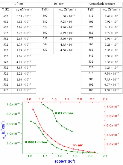
Figure 6 shows the variation of σdc against 1000/T for nanoparticle compacts of CaWO4 samples
measured at reduced air pressure of 10-4, 10-2 torr and atmospheric pressure. The results of the
measurements are summarized in table 1. At atmospheric pressure, the value of dc conductivity of
compacted pellets of nanocrystalline CaWO4 increased from 3.68 ×10⁻¹⁰ Ω-1cm-1 to 9.48 ×10⁻⁹
Ω-1cm-1 when the temperature was raised from 482 to 612 K. At a pressure of 10-2 torr, the dc
conductivity of the specimen increased from to 4.5 ×10⁻¹¹ Ω-1cm-1 to 1 ×10⁻¹⁰ Ω-1cm-1 as the
temperature was raised from 532 to 592 K. With a pressure of 10-4 torr, the dc conductivity
increased from 1.08 ×10⁻¹² Ω-1cm-1 to 6.53 ×10⁻¹¹ Ω-1cm-1 when the temperature was increased
from 492 to 622 K. Thus as the pressure is decreased there is reduction in the dc conductivity of the
pellet sample. In order to study the effect of grain size on dc conductivity and its variation with
temperature, conductivity measurements were performed on compacted pellets of nanoparticles of
CaWO4 having two different grain sizes. The variation of σdc against 1000/T for compacted
nanoparticles of CaWO4 of two different grain sizes, 13 and 26 nm is shown in figure 7. For the
pellet sample with grain size 26 nm the conductivity increased from 4.16 × 10⁻⁹ Ω-1cm-1 to 1.02 ×
10–7 Ω-1cm-1 as the temperature was increased from 482 to 612 K while for the sample with grain
temperature was increased from 482 to 612 K (Table 2). It is observed that for a particular
temperature, the dc conductivity values showed an increase for the pellet sample with higher grain
size compared to sample with lower grain size. DC conductivity measurements were also performed
on heat treated pellet. The variation of σdc with temperature of unannealed and annealed compacted
samples of nanostructured CaWO4 is shown in figure 8. The measured dc conductivity of
nanoparticle compacts of CaWO4 heat treated for 2 hours at 300 ºC, exhibited an increase from 8.28
×10–10 Ω-1cm-1 to 1.37 ×10⁻⁸ Ω-1cm-1 as the temperature was increased from 482 to 612 K (Table 3).
The conductivity of compacted nanoparticles of CaWO4 annealed for 2 hours at 300 ºC showed
marginal enhancement compared to unannealed pellet.
Figure 5 V-I graphs for compacted nanoparticles of CaWO4
Arrhenius behaviour, where an exponential dependence exists between the conductivity and
temperature is widely reported in literature6,28,29. The temperature dependence of resistivity is given
by the Arrhenius equation
EakT
exp
0
(3)
where ρ0 is the pre-exponential factor with the dimensions of Ω cm, k the Boltzmann constant, Ea is
the activation energy and T is the absolute temperature. Petrov et al. 30 reported the electrical
conduction behaviour of single crystals of CaMoO4, which has a structure similar compared to that
of PbMoO4. From tracer diffusion studies on CaMoO4 and CaWO4 it has been shown that the
diffusion of the isotope 185W is considerably faster than that of 45Ca. Also from the diffusion
faster than that of molybdenum. On the basis of this it has been assumed that oxygen ions are the
most mobile ionic species in CaMoO4. In the case of nanocrystalline CaWO4, all the pellet samples
exhibited Arrhenius behaviour. The increase in the dc conductivity with temperature is due to the
increase in the thermally activated drift mobility of the charge carriers.
Table 1Temperature dependent variation of DC conductivity (σdc) of nanocrystalline CaWO4 of average grain
size 13 nm under different pressures (sample code: CT1).
10-4 torr 10-2 torr Atmospheric pressure
T (K) dc (-1cm-1) T (K) σdc(Ω−1cm−1) T (K) σdc(Ω−1cm−1)
622 6.53 × 10⁻¹¹ 592 1.00 × 10⁻¹⁰ 612 9.48 × 10⁻⁹
612 6.12 ×10⁻¹¹ 582 9.28 × 10⁻¹¹ 602 7.92 × 10⁻⁹
602 5.16 ×10⁻¹¹ 572 8.80 × 10⁻¹¹ 592 6.11 × 10⁻⁹
592 3.77 ×10⁻¹¹ 562 6.49 × 10⁻¹¹ 582 4.77 × 10⁻⁹
582 2.65 ×10⁻¹¹ 552 5.60 × 10⁻¹¹ 572 3.96 × 10⁻⁹
572 1.75 ×10⁻¹¹ 542 4.95 × 10⁻¹¹ 562 3.21 × 10⁻⁹
562 1.09 ×10⁻¹¹ 532 4.50 × 10⁻¹¹ 552 2.55 × 10⁻⁹
552 7.26 ×10⁻¹² 542 1.99 × 10⁻⁹
542 4.85 ×10⁻¹² 532 1.53 × 10⁻⁹
532 3.15 ×10⁻¹² 522 1.24 × 10⁻⁹
522 2.22 ×10⁻¹² 512 9.54 × 10⁻¹⁰
512 1.96 ×10⁻¹² 502 7.45 × 10⁻¹⁰
502 1.53 ×10⁻¹² 492 6.07 × 10⁻¹⁰
492 1.08 ×10⁻¹² 482 3.68 × 10⁻¹⁰
Figure 6 Temperature dependent variation of σdc of nanocrystalline CaWO4 samples for different pressures
Table 2: Temperature dependent variation of DC conductivity (σdc) of nanocrystalline CaWO4 of different
average grain sizes in air
13 nm 26 nm
T (K) σdc(Ω
−1
cm−1) T (K) σdc(Ω
−1
cm−1)
612 9.48 × 10⁻⁹ 612 1.02 × 10⁻⁷
602 7.92 × 10⁻⁹ 602 8.03 × 10⁻⁸
592 6.11 × 10⁻⁹ 592 6.40 × 10⁻⁸
582 4.77 × 10⁻⁹ 582 5.03 × 10⁻⁸
572 3.96 × 10⁻⁹ 572 4.10 × 10⁻⁸
562 3.21 × 10⁻⁹ 562 3.21 × 10⁻⁸
552 2.55 × 10⁻⁹ 552 2.52 × 10⁻⁸
542 1.99 × 10⁻⁹ 542 1.85 × 10⁻⁸
532 1.53 × 10⁻⁹ 532 1.44 × 10⁻⁸
522 1.24 × 10⁻⁹ 522 1.13 × 10⁻⁸
512 9.54 × 10⁻¹⁰ 512 8.45 × 10⁻⁹
502 7.45 × 10⁻¹⁰ 502 6.74 × 10⁻⁹
492 6.07 × 10⁻¹⁰ 492 5.27 × 10⁻⁹
482 3.68 × 10⁻¹⁰ 482 4.16 × 10⁻⁹
Figure 7 Temperature dependent variation of σdc of nanocrystalline CaWO4 samples having different grain
Table 3: Temperature dependent variation of DC conductivity (σdc) of nanocrystalline CaWO4 of average grain
size 13 nm for unannealed sample and sample annealed for 2 hrs. at 300 °C in air. as prepared 2 hrs
T (K) σdc(Ω
−1
cm−1) T (K) σdc(Ω
−1
cm−1)
612 9.48 × 10⁻⁹ 612 1.37 × 10⁻⁸
602 7.92 × 10⁻⁹ 602 1.17 × 10⁻⁸
592 6.11 × 10⁻⁹ 592 9.99 × 10⁻⁹
582 4.77 × 10⁻⁹ 582 7.70 × 10⁻⁹
572 3.96 × 10⁻⁹ 572 6.73 × 10⁻⁹
562 3.21 × 10⁻⁹ 562 5.49 × 10⁻⁹
552 2.55 × 10⁻⁹ 552 4.18 × 10⁻⁹
542 1.99 × 10⁻⁹ 542 3.17 × 10⁻⁹
532 1.53 × 10⁻⁹ 532 2.61 × 10⁻⁹
522 1.24 × 10⁻⁹ 522 2.14 × 10⁻⁹
512 9.54 × 10⁻¹⁰ 512 1.67 × 10⁻⁹
502 7.45 × 10⁻¹⁰ 502 1.36 × 10⁻⁹
492 6.07 × 10⁻¹⁰ 492 1.05 × 10⁻⁹
482 3.68 × 10⁻¹⁰ 482 8.28 × 10⁻¹⁰
Figure 8 Temperature dependent variation of σdc of unannealed and annealed nanocrystalline CaWO4
Density functional calculations using linearised-augmented-plane-wave method was
reported for scheelite molybdates and tungstates by Zhang et. al. 31. The results indicate that
CaWO4 has a direct band gap at the centre of the Brillouin zone. DC and ac electrical conductivities
were used to characterize the type of charge transport in single crystals of CaWO4 which were
equilibrated with H2-H2O-Ar gas mixtures25. Measurements were made from 900° to 1300°C and at
PH2O/PH2 ratios from 0.02 to 3.0. The ac conductivity at 1000°C varied from 51.4×10 6 to
5.89×10 6 mho/cm for PH2O/PH2=0.02 and 2.0, respectively; the dc conductivity changed from 51.0
×10 6 to 5.42 ×10 6 mho/cm under the same experimental conditions25. The results were described
by a paired-defect model of oxygen vacancies and oxygen interstitials. In the present study, it was
observed that for compacted nanoparticles of CaWO4 the dc electrical conductivity was about two
orders of magnitude lesser compared to that reported for single crystals of CaWO4. In the case of
compacted nanoparticles of CaWO4 the dc electrical conductivity values increased with increase in
temperature. This is in agreement with already reported behaviour of variation of electrical
conductivity with temperature for single crystals of CaWO4.
The optical properties like the absorption, photoluminescence and reflectance spectra
exhibited by CaWO4 are described in terms of charge transfer transitions in the WO42− tetrahedra22,
23
. Conductivity measurements indicated that the dc conductivity of as compacted pellets of
nanoparticles of CaWO4 is sensitive to air pressure (Table 1). There is a possibility of presence of
large fraction of surface defects in the form of oxygen vacancies in the pellet sample. These surface
defects play a crucial role in determining the conductivity of the pellet sample. In the presence of
air, these oxygen vacancies will be replenished to form the correct stoichiometry. The dc
conductivity of nanocrystalline CaWO4 pellet sample with grain size 26 nm was found to be
increased compared to pellet sample with grain size 13 nm (Table 2). It is well known that the band
gap of a material increases with reduction in grain size 27. This phenomenon of quantum size effect
is widely reported in literature27, 32, 33. This phenomenon and its impact on the optical properties is
reported in the case of nanostructured CaWO4 34-38. As a result of widening of band gap, more
energy is needed for creating free charge carriers. The band gap of nanocrystalline CaWO4 of grain
size 13 nm is larger compared to the sample with grain size 26 nm. It is seen that the conductivity of
compacted nanoparticles of CaWO4 of grain size 13 nm is marginally enhanced with heat treatment
of the pellet in air at a temperature of 300 °C for 2 hours compared to unannealed pellet (Table 3).
The annealing temperature was specifically kept low so that no appreciable grain growth occurs.
The change observed in the dc conductivity of the sample is due to factors other than grain growth.
This low temperature annealing in air can introduce significant changes in the density of defects
the dc conductivity of the specimen considerably. The conductivity of annealed pellet sample was
found to have a marginal increase compared to that of unannealed pellet sample. The value of
conductivity at 612 K recorded an increase from 9.48×10⁻⁹ Ω-1cm-1 for the unannealed pellet to
1.17×10⁻⁸ Ω-1cm-1 for the pellet heat treated for 2 hours (Table 3). Upon heat treatment, the pore
density of the specimen reduced and the pellet become more rigid compared to unannealed pellets
resulting in better contacts between individual grains. This may be the possible reason of
enhancement of conductivity of the heat treated pellet samples of CaWO4.
CONCLUSION
Nanocrystalline calcium tungstate of two different grain sizes 13 and 26 nm were
synthesized using aqueous chemical precipitation method. The crystal structure and grain size of
different samples were determined using x-ray diffraction data. The effect of microstrain on
broadening of X-ray diffraction peak was eliminated using Hall-Williamson analysis. Transmission
electron microscopy was also used to estimate the particle size distribution and morphology. The
lattice planes were clearly visible in high resolution transmission electron microscope images
indicating good crystallinity of the samples in agreement with XRD analysis. The interplanar
spacings measured from HRTEM images agree well with the data obtained from X-ray diffraction
patterns. The sharp rings obtained in the electron diffraction pattern showed that the samples were
crystalline.
DC conductivity measurements were done on compacted pellets of nanocrystalline samples
of CaWO4. It was found that the dc conductivity showed an exponential increase with temperature
exhibiting Arrhenius behaviour for all the samples. For nanoparticle compacts of CaWO4, the
measured dc conductivity was about two orders of magnitude less than that reported for single
crystals of CaWO4. Also, the dc conductivity showed an increase with increase in average grain size
of the sample. The conductivity measurements performed on pellet heat treated for two hours at a
low temperature of 300°C exhibited enhancement in dc conductivity compared to unannealed green
pellet. This enhancement as a result heat treatment may be due to reduction of porosity which
results in better contact between grains.
ACKNOWLEDGEMENT
:
The author acknowledges the guidance given by Prof. M AbdulKhadar, Professor (Emeritus) Centre for Nanoscience and Nanotechnology, University of Kerala.
REFERENCES
1. Mohanraj VA, Chen Y. Nanoparticles – A review. Trop. J. Pharma. Res. 2006; 5(1):
561-573.
2. Clemens B, Xiaoba C, Radha N, Mostafa AE. Chemistry and properties of nanocrystals of
different shapes. Chem. Rev. 2005; 125: 1025.
3. Xuebin Y, Zeiwi T, Dalin S, Liuzhang O, Min Z. Recent advances and remaining challenges
of nanostructured materials for hydrogen storage applications. Prog. Mater. Sci. 2017; 88: 1.
4. Ovidko IA, Valiev RZ, Zhu YT. Review on superior strength and enhanced ductility of
metallic nanomaterials. Prog. Mater. Sci. 2018; 94: 462-540.
5. Ukoba KO, Eloka-Eboka AC, Inambao FL. Review of nanostructured NiO thin film using
the spray pyrolysis technique. Renew. Sust. Energy Rev. 2018; 82: 2900-2915.
6. Biju V, Abdul Khadar M. DC conductivity of consolidated nanoparticles of NiO. Mater.
Res. Bull. 2001; 36: 21-33.
7. Matthew RD, Joshua M, George SN, Ayusman S, John VB. Thermal and electrical
conductivity of bismuth telluride nanoparticles. Small 2009; 5: 933-937.
8. Saafan SA, Meas TM, El-Ghazzawy EH et al. AC and DC conductivity of NiZn ferrite
nanoparticles in wet and dry conditions. J. Magn. Magn. Mater. 2010; 322: 2369-2374.
9. Bargougui R, Bouazizi N, Ben Soltan W et al. Controlled synthesis and electrical
conduction properties of anatase TiO2 nanoparticles via polyol method. Appl. Phys. A 2016;
22: 309.
10.Shobhna C. Structural, morphological, thermal, dielectric and electrical properties of
alumina nanoparticles of filled PVA-PVP blend matrix-based polymer nanocomposites.
Polym. Compos. 2018; 39: E1788-E1799.
11.Chiang YM, Lavik EB, Blom DA. Defect thermodynamics and electrical properties of
nanocrystalline oxides : pure and doped CeO2. Nanostruct. Mater. 1997; 9: 633-642.
12.Lu K, Wang JT, Wei WD. Comparison of properties of nanocrystalline and amorphous Ni-P
alloys. J. Phys. D: Appl. Phys. 1998; 25: 808.
13.Sivakumar N, Narayanasamy A, Shinoda K, Chinnasamy CN, Jeyadevan B. Electrical and
magnetic properties of chemically derived nanocrystalline cobalt ferrite. J. Appl. Phys.
2007;10: 013916.
14.Abdulkhadar M, Binny Thomas. DC conductivity of nanoparticles of CdS and ZnS.
15.Brus L. Electronic wave functions in semiconductor clusters: Experiment and Theory. J.
Phys. Chem. 1986; 90: 2555-2560.
16.Lijuan C, Liping L, Guangshe L. Surface hydration-mediated conduction of NiO
nanocrystals. Solid State Ion. 2008; 179: 712-717.
17.Anindita B, Soumen B, Sourish B, Dipankar .C. Electrical properties of compacted
assembly of copper oxide nanoparticles. J. Appl. Phys. 2005; 98: 074307.
18.Das D, Chakravorty D. Interfacial conduction in silica gels containing nanocrystalline
copper oxide. Appl. Phys. Lett. 2000; 76: 1273.
19.Nan C, Tschope A, Holten S, Kleim H, Birringer R. Grain-size dependent electrical
properties of nanocrystalline ZnO. J. Appl. Phys. 1999; 85: 7735.
20.Babita B, Kishore Kumar D, Manorama SV. Hydrothermal synthesis of highly crystalline
ZnO nanoparticles : A competitive sensor for LPG and EtOH. Sens. Actu. B : Chem. 2006;
119: 676-682.
21.Porto SPS, Scott JF. Raman Spectra of CaWO4, SrWO4, CaMoO4 and SrMoO4. Phys. Rev.
1967; 157(3): 716.
22.Treadway MJ, Powell RC. Luminescence of calcium tungstate crystals. J. Chem. Phys.
1974; 61: 4003.
23.Grasser R, Pitt E, Zimmerer G. Optical properties of CaWO4 and CaMoO4 crystals in the 4
to 25 eV region. Phy. Stat. Sol., (b) 1975; 69: 359-368.
24.Groenink JA, Binsma H. Electrical conductivity and defect chemistry of PbMoO4 and
PbWO4. J. Sol. State Chem. 1979; 29: 227-236.
25.Rigdon MA, Grace RE. Electrical charge transport in single-crystal CaWO4. J. Amer.
Ceram. Soc. 1979; 29: 227.
26.Williamson GK, Hall WH. X-ray line broadening from filed aluminium and wolfram. Acta
Metall. 1953; 1: 22-31.
27.Anandakumar VM, Abdul Khadar M. Synthesis, characterization and optical properties of
nanocrystalline lead molybdate. Phys. Stat. Sol. (a) 2008; 205: 2666-2672.
28.Balachandran U, Eror NG. Electrical conductivity in strontium titanate. J. Solid State Chem.
1981; 39: 351-359.
29.Rhimi T, Leroy G, Duponchal B, Khirouni K, Guermazi S, Toumi M. AC and DC
conductivity studies of LiH2PO4 compound using impedance spectroscopy. Ionics 2018; 24:
1305-13012.
30.Petrov A, Kofstad P. Electrical conductivity of CaMoO4. J. Sol. State Chem. 1979; 30:
31.Zhang Y, Holzwarth NAW, Williams RT. Electronic band structures of the scheelite
materials CaMoO4, CaWO4, PbMoO4 and PbWO4. Phys. Rev. B 1998; 57: 12 738 -12750.
32.Rajeev RP, Abdul Khadar M. Characterization of chemically synthesized CdS nanoparticles.
Pramana – J. Phys. 2005; 65: 801-807.
33.Kanade KG, Kale BB, Aiyer RC, Das BK. Effect of solvents on the synthesis of nano-size
zinc oxide and its properties. Mater. Res. Bull. 2006; 41: 590-600.
34.Lou Z, Cocivera M. Cathodoluminescence of CaWO4 and SrWO4 thin films prepared by
spray pyrolysis. Mater. Res. Bull. 2002; 37: 1573-1582.
35.Chen D, Guozhen S , Kaibin T, Huagui Z, Yitai Q. Low temperature synthesis of metal
tungstates nanocrystallites in ethylene glycol. Mater. Res. Bull. 2003; 38: 1783-1789.
36.Cavalcante LS, Longo VM, Sczancoski JC, Almaida MAP et al. Electronic structure, growth
mechanism and photoluminescence of CaWO4 crystals. CrystEngComm 2012; 14: 853-868.
37.Valeria ML, Lourdes G, Daniel GS et al. A joint experimental and theoretical study of
nanomorphology of CaWO4 crystals. J. Phys. Chem. 2011; 115: 20113-20119.
38.Thongtem T, Phuruangrat A and Thongtem S. Synthesis of CaWO4, SrWO4 and BaWO4
with nanosized particles using cyclic microwave radiation. J. Ceram. Proc. Res. 2008; 9(3):