I
.
Univac@
LARC
PROCESSOR
DISPATCHER
I
~7ILuuL~®
AUGUST 1960
COPY NO. 55
Univac@
LARC
PROCESSOR
DISPATCHER
COMP ANY CONFIDENTIAL Registered Circulation
The information contained in this publication is the prQP-erty of the Sperry Rand Corporation. It is submitted in confidence and must not be disclosed to others except in con-fidence with the written permission of an officer of the Remington Rand Univac Division, Sperry Rand Corpora-tion. This copy, issued in your name, is not to be reproduced or duplicated without permission in writing from a duly authorized representative of the Sperry Rand Corporation. This pUblication is subject to recall.
~""RIuuL~~
DIVISION OF SPERRY RAND CORPORATION
This manual has been reviewed by the engineer-ing design staff and approved for issue.
Suggestions for additions, deletions, correc-tions, or improvements to this manual should be for-warded to
Publications Engineering Group (120)
Remington Rand Univac
Division of Sperry Rand Corporation
Box 5616
Heading
1 ... 1. 1-2. 1-3. 1-4. 2-1. 2-2. 2-3. 2-4. 2-5. 2-6. 2-7. 2-8. 2-9. 2-10. 2-11. 2-12. 2-13. 3-1. 3-2. 3-3. 3-4. 3-5.
CONTENTS
TitleSECTION I. INTRODUCTION
Scope of This Manual • •
· .
. .
The Dispatcher: General • • •Main Functions • • • • • • • • • General Description
· .
. .
·
.
.
.
·
.
SECTION II. PRIORITY CIRCUITS
General
.
. .
.
.
. ·
·
·
· ·
· ·
Priority Within the Memory
·
·
· ·
·
Overflow and Underflow •· · · ·
•·
Order of Priority.
·
· ·
·
·
·
· · ·
Special Underflow Precautions for DrumWrite Synchronizers
·
· ·
· ·
Operation of Priority Circuits· ·
·
Avoiding Time-Slot Waste·
· ·
· ·
Conditions of Priority
·
· · ·
·
· ·
·
·
Synchronizers Other Than DrumSynchronizers
· · ·
· · · ·
·
· · · ·
Drum Read Synchronizers 1, 2, and 3(Sl, S2, SO)
· · · ·
·
Drum Write Synchronizer 1 (S3) Drum Write Synchronizer 2 (S4) Order of Time-Slot Assignment: Examples
SECTION III. ADDRESS AND BUFFER REGISTERS
General • • • • • • • • • • • • Basic Characteristics ••
Address-Register Matrix • • •
Input-Buffer-Register Matrix • • • Output-Buffer-Register Matrix
.
. . . .
.
. .
Page 1-1 1-1 1-3 1-3 2-1 2-1 2-2 2-2 2-3 2-4 2-5 2-6 2-6 2-7 2-9 2-10 2-11 3-1 3-1 3-2 3-4 3-9SECTION IV. ADDRESS AND INPUT-OUTPUT BUFFER CONTROLS
4-1. 4-2. 4-3.
General • • • • • • • • • Address-Transfer Control
First Section • • •
Heading Title Page
4-4. Second Section • • • • • • • • • • 4-4 4-5. Address-Register and Buffer-Register
Controls • • • • • • • • • • • • • • 4-5 4-6. Address- and Buffer-Register Control
for an Input Synchronizer j (Other 4-5 Than Tape) • • • • • • • • • • • • • 4-5 4-7. Address- and Buffer-Register Control
for an Output Synchronizer j (Other
Than Tape) • • • • • • • • • • • • • 4-9 4-8. Address- and Buffer-Register Control
for Tape Input-Output Synchronizer j 4-10 4-9. Timing for Address and Input-Output Buffer
5-1. 5-2. 5-3. 5-4. 5-5. 5-6. 5-7. 5-8. 5-9. 5-10. 5-11. 5-12. 5-13. 5-14. 5-15. 5-16. 5-17 • 6-1. 6-2. 6-3.
Controls • • • • . • • • • • • • . • • • . 4-11
SECTION V. SYNCHRONIZER ADDRESS MODIFIER
General • • • • • • • • • • • .
Capabilities of Address Modifier.
Pattern of Modification • • • • • • • • • • Address-Modifier Controls
Functions of a Digit Adder-Subtractor • • • Digit 1 Adder-Subtractor • • • • • • • •
Translating the Input Digit • • • • • • Modifying the Translated Digit
Determining How Modification Affects Digit 2 • • • • • • • • • • • • • • • Translating Modified Digit Back to Larc
Code • • • • • • • • • • • • • • • •
Differences Between Adder-Subtractors • • • Differences in Translation • • • • Differences in Modification • • •
Binary-Modification Detection Parity-Modification Detection Difference in Retranslation • • • • Address-Modifier Timing • • • • • • ••
SECTION VI. TYPICAL WORD-TRANSFER SEQUENCES
General •• • • Word Transfer 1
Word Transfer 2
.
.
.
Figure 1-1. 2-1. 2-2. 2-3. 2-4. 2-5. 2-6. 3-L 3-2. 3-3. 3-4. 3-5. 4-1. 4-2. 4-3. 4-4. 4-5. 4-6. 4-7. 5-1. 5-2. 5-3. 5-4. 5-5. 5-6.
ILLUSTRATIONS
TitleThe Dispatcher: Simplified Block Diagram •• Priority Circuit For Synchronizer Other
Than Drum Synchronizer: Simplified Logic • Priority Circuit for Drum Read Synchronizer: Simplified Logic • • • • • • • • • • • • • Priority Circuit for Drum Write Synchronizer
1 (53): Simplified Logic • • • • • • • • • Priority Circuit for Drum Write ·Synchronizer 2 (54): Simplified Logic • • • • • • • • • Example of Time-Slot Assignment for Drum
Read Synchronizers 1, 2, and 3 (51, 52,
SO) • • • • • • • • • • • • • • • • • • •
Examples of Time-Slot Assignment for Drum Read Synchronizer 1 (51), Drum Write Synchronizer 1 (53), and Line-Printer Synchronizer 2 (56) • • • • • • • • • Core Windings: Schematic • • • • • • • • • • Address-Register Matrix: Simplified Diagram Timing of Read-Write Cycle of an Address
Register • • • • • • • • • • • • • • • • • Half Registers of Drum Read Synchronizers 1
and 2 (Sl, 52) • • • • • • • • • • • • • • Half Registers of Drum Write Synchronizer 1
(S3) and Line-Printer Synchronizer 1 (55)
Address-Transfer Control. Part 1 • • • • • Address-Transfer Control. Part 2 • • • • • Address- and Buffer-Register Controls for an Input Synchronizer j: Detailed Logic • • • Address- and Buffer-Register Controls for an
Output Synchronizer j (Two Buffer Regis-ters): Detailed Logic • • • • • • • • • • Address- and Buffer-Register Controls for
Tape Input-Output Synchronizer j: Detailed
Logi c . • • • • • • • • . • • • • • . • .
Memory-Transfer Control Cycle for Input Synchronizer j • • • • • • • . • • • • Memory-Transfer Control Cycle for Output
Synchronizer j • . . . • • • • • • . • • • Synchronizer Address Modifier: General Block Diagram • • • • • • • • • • • • • • • •• Pattern of Modification by Add 1, Subtract 1,
or No Change • • • • • • • • • •• • • • Derivation of Control Signals • • • • • • • Digit 1 Adder-Subtractor: Simplified Logic. Derivation of Quinary Result of 2 ••
Address Modification: Timing Diagram • • •
Figure
6-l. 6-2.
Title
Typical Word-Transfer Sequences • • • • • • The Dispatcher: Simplified Logic Diagram
Note on
ENGINEERING DRAWINGS
Larc Dispatcher
Page
6-2 6-3
The following engineering drawings are referred to by number in figure 6-2 and alluded to throughout the text. They are listed here appropriately divided by section for this manual and by subject.
Section lOP Disprtcher: General Block Diagram
Section II lOP Priority Circuits. Part IA
lOP Priority Circuits. Part II
lOP Pri~city Circuits. Part III lOP Priority Circuits. Part IV
W.E.C. Priority, Address, and Buffer Register Controls. Part IA
Section III lOP Synchronizer Address Register
lOP Input Buffer Register. Part I lOP Input Buffer Register. Part II
lOP Input Buffer Register Expanded System. Part III lOP Input Buffer Register Expanded System. Part IV lOP Output Buffer Register. Part I
lOP OutputBuffer Register. Part II
lOP Output Buffer Register Expanded System. Part III lOP Output Buffer Register Expanded System. Part IV
Section IV lOP Address Register Output Inverters
lOP Synchronizer Address Pulseformers. Part I lOP Synchronizer Address Pulseformers. Part II Synchronizer Address Recirculation Gates
lOP Synchronizer Address Transfer Control. Part IV
D 809 411
D 807 520 D 807 521 D 807 522 D 807 523 D 807 544
D 807 534 D 807 560 D 807 561 D 807 562 D 807 563 D 807 564 D 807 565 D 807 566 D 807 567
D 807 529
D 807 530
D D07 531
D 007 532
lOP Address and Buffer Register Control Drum Read Synchronizers 1 and 2
IOP Address and Buffer Register Controls Drum Write Synchronizers 3 and 4
lOP Address and Buffer Register Control Line Printers lOP Address and Buffer Register Control Card Reader and
Charactron
W.E.C. Priority, Address, and Buffer Register Controls. Part IA
lOP Addressand Buffer Register Control Tape Read-Write Synchron i zer 1
lOP Address and Buffer Register Control Tape Read-Write Synchronizer 2
lOP Address and Buffer Register Control Tape Read-Write Synchronizer 3
lOP Address and Buffer Register Control Tape Read-Write Synchronizer 4
lOP Synchronizer Memory Address Control. Part V Section V
Synchronizer Address Modifier Controls. Part II Synchronizer Address Modifier Control. Part I Synchronizer Address Modifier. Part IA Synchronizer Address Modifier. Part IB lOP Synchronizer Address Modifier. Part IIA Synchronizer Address Modifier. Part lIB lOP Synchronizer Address Modifier. Part IlIA lOP Synchronizer Address Modifier. Part IIIB lOP Synchronizer Address Modifier. Part IVA Synchronizer Address .Modifier. Part IVB Synchronizer Address Modifier. Part VA Synchronizer Address Modifier. Part VB
Table 2-1. 3-1. 5-1. 5-2.
TABLES
TitleOrder of Time-Slot Priority of Synchronizers Number and Type of Buffer Registers for Each Synchronizer • • • • • • • • • • • • Address-Modifier Control Signals • • •
Comparison of Larc and Seven-Bit Codes • • •
D 807 550
D 807 551
D 807 552
D 807 553
D 807 554
D 807 555
D 807 556
D 807 557
D 807 558
D 807 559
D 807 535
D 807 536
D 807 540
D 807 541
D 807 542 D 807 543
D 807 544
D 807 545
D 807 546
D 807 547
D 807 548
D 807 549
1·1. SCOPE OF THIS MANUAL
SECTION I
INTRODUCTION
The primary purpose of this manual is to provide training and refer-ence information about the theory of operation of the logical circuits in the dispatcher section of the Larc processor. It applies equally to any Larc system. from the basic to the fully expanded. It does not, however, describe the physical characteristics of the system or the detailed circuit operation of basic logic elements such as gates, delay flops, and pulse-formers. Information on circuitry and the properties of these elements is available in Larc Circuitry, Section I, Standard Logic-Circuitry Types.
For practical reasons not every detail of every logical operation is described in this manual, but the content should provide the reader with the necessary background information for tracking down details on the en-gineering drawings, which define completely the logic of the dispatcher.
1·2. THE DISPATCHER: GENERAL
The dispatcher is a closely integrated group of circuits which coor-dinates and controls all data transfers to and from the memory for all of the synchronizers except the console-printer synchronizer.*
A summary of the major functions and a general description of the dis-patcher follow in this section. The description is based on and illustrat-ed by the block diagram of figure 1-1. Sections II through V contain more detailed descriptions and illustrations of each of the subdivisions of the dispatcher, which are indicated by the blocks in figure 1-1. The descrip-tions of the dispatcher subdivisions provide the reader with the background for understanding Section VI, which describes the coordinated operation and timing of all sections of the dispatcher in performing typical sequences of memory transfers for the synchronizers. Both the detailed descriptions of
the dispatcher subdivisions and the description of the sequences of trans-fer operations are illustrated by the simplified logic diagram of figure 6-2 and the timing diagram of figure 6-1.
.-I N
WORD TRANSFER REQUEST FROM SYNCHRONIZER j
MNB FROM MEMORY
NOTES
j = NUMBER OF ANY SYNCHRON I ZER - - CONTROL LINES - - ADDRESS LINES - INFORMATION
PRIORITY CIRCUITS
Priority Achieved ADDRESS
I---~---~---~TRANSFER
1---1~ READ SIGNAL TO MEMORY
Memory Access Achieved
TO rPI
Regeneration
CONTROLS
--®-
---~--TO MEMORY - - ADDRESS
DECODER
L __ -
+-
~a~-lI I
I
ADDRESS AND Reod Control BUFFER
-REGISTER CONTROLS
Write Control
Read Control
Write Control
ADDRESS REGISTERS
$
NPUT J . PFRS 1 I FROM rPI I II
J
ADDRESS-MODIFIER CONTROLS ADDRESS MODIFIER_ _ ~odified ~ddre~ _
J
r -________ ~60~---. . TO MEMORY WRITE BUS
I NPUT BUFFER REGISTERS
WRITE ]
CONTROL FROM INPUT SYNCHRONIZER DATA
READ CONTROL FROM
\ 4 - - - OUTPUT SYNCHRONIZER
DATA TO OUTPUT S YNCHRON I ZER
FROM MEMORY READ BUS
4775
1-3. MAIN FUNCTIONS
These are the main functions of the dispatcher.
(1) To define. on the basis of preassigned priority ratings. the time and order in which memory transfers requested by the synchronizers will be performed.
(2) To store a memory address for each operating synchronizer and use the address to initiate a memory-transfer operation requested by the syn-chronizer.
(3) To modify the memory address after each memory reference and. af-ter access to the memory is assured. store the modified address in prepar-ation for the next memory reference for the synchronizer.
(4) To regenerate the address for another attempt if access to the memory is denied.
(5) To control the transfer of data between the memory bus and a buf-fer register for the synchronizer.
(6) To inform the synchronizer of the completion of the transfer and of any errors detected while the transfer was being m~de.
1-4. GENERAL DESCRIPTION
The dispatcher is essentially an auxiliary of the synchronizers for dispatching input-output data between the memory and a number of input or output buffer registers associated with the synchronizers (figure 1-1). There are from one to four l2-digit buffer registers within the dispatcher
for each synchronizer in the system; they are tape-wound magnetic-core reg-isters. The cores of the input and output registers are arranged in sep-arate matrices. They provide temporary storage for data being transferred between the memory and an input-output device and provide the means by which the data are converted from serial-parallel to parallel form or from parallel to serial-parallel form.
The flow of data between the buffer registers and the input-output de-vices is controlled by the synchronizers. The rate and order of flow is governed primarily by the characteristics and operating mode of the partic-ular synchronizer and input-output device concerned. In most cases data are transferred to or from a buffer register by a synchronizer one digit at a time. The time interval between digits is dependent on the reading or recording rate of the synchronizer.
Whenever a synchronizer completes the processing and transfer of a word of data to or from a buffer register. it signals the dispatcher to
(1) Transfer the word to the main memory if it is an input
synchron-izer, or
(2) Obtain a new word from memory if it is an output synchronizer.
Since the synchronizers process data asynchronously with respect to one an-other. several may signal the dispatcher at the same time for a transfer of data. Such conflicts are resolved by priority circuits within the dispatch-er which detdispatch-ermine. on the basis of preassigned priority ratings. the orddispatch-er in which the data will be transferred for the synchronizers. The priority rating assigned to a synchronizer reflects. in general, the rate at which the synchronizer must have information transferred in order to maintain without interruption the flow of data required by the input-output device.
The synchronizers and the dispatcher together are designed to process a number of words of input-output data automatically without direct inter-vention by the processor program. For example. once it is started. a drum read synchronizer with the aid of the dispatcher reads from a drum and trans-fers a multiple of 100 words of data to successive locations in the memory. To accomplish this. means must be available to the dispatcher for keeping track of the memory address of every word transferred. The dispatcher there-fore contains for each synchronizer a register in which is stored for the synchronizer the memory address of the next word to be transferred to or from the memory. Whenever the synchronizer signals for and receives prior-ity, this address is read out of the address register and sent to the mem-ory-address decoder to initiate a word-transfer operation. The address is also sent to an address modifier where it is modified before being written back into the same register after access to the memory is assured. The modified address then is the address of the next word to be transferred for the synchronizer.
The beginning memory address for a particular input-output operation is supplied by the processor program. Instructions are provided for trans-ferring a beginning address from register PI to anyone of the address reg-isters or for transferring the contents of any address register to register Pl. The latter transfer is normally made to perform a program check on the address.
The address modifier is a special-purpose adder-subtractor which is time-shared to modify addresses for the input-output operations of all the synchronizers. Because data transfers are usually made to or from succes-sive memory locations in ascending order. an address will, in most cases, be modified by adding 1. However, depending upon the type of synchronizer and the mode in which it is operating, an address is sometimes modified by subtracting a number or by adding a number other ·than 1. For example, dur-ing a backward tape-read operation the number 1 is subtracted from the ad-dress. Mode signals indicating what number is to be added or subtracted from the address are sent to the address-modifier controls by the synchron-izers.
After initiating a word-transfer operation for a synchronizer by send-ing an address to the memory-address decoder, the dispatcher subsequently completes the transfer, provided that the memory is not busyr The transfer is completed during an input operation through reading the word out of an input-buffer register of the synchronizer and sending it to the memory over the write bus. During an output operation the word is received from the memory over the read bus and is written into an output-buffer register of
the synchronizer. When a word-transfer operation is completed, the dis-patcher signals the appropriate synchronizer. If a memory-select or HSB odd-even error is detected during the transfer operation, the dispatcher sends an error signal to the appropriate synchronizer.
2-1. GENERAL
SECTION II
PRIORITY CIRCUITS
Every 2 ~s the synchronizers as a group are allotted a O.5-~s time slot, during which anyone synchronizer is permitted to attempt a word transfer over the memory high-speed-bus system. Since the synchronizers process information asynchronously with respect to one another. more than one syn-chronizer may require access to the memory at the same time. The priority circuits are therefore designed to remedy this problem by determining which synchronizer shall use the time slot on a basis of preassigned priority. This system of priority ratings reflects primarily the characteristic data-transfer ra~es of the input-output devices controlled by the synchronizers. so that the faster an input-output device. the higher the memory-access priority allotted to its synchronizer. Priority ratings also depend, though to a lesser extent, upon the buffer-storage capacity of the various syn-chronizers--that is, whether a synchronizer has one or two buffer registers.
2-2. PRIORITY WITHIN THE MEMORY
In transferring information a synchronizer may be required not only to compete with other synchronizers for the available time slots but also to compete with other synchronizers, the computing unit. and the central pro-cessor for access to a particular memory unit.
Consequently. even though a time slot is assigned to a synchronizer on a priority basis. it may still be wasted. which results in a delay in the transfer of a word if the memory unit addressed happens to be busy. Al-though the programmer will avoid, in general. simultaneous reference to the sa.me memory unit by two or more of the sections of the system (computing units. central processor. or dispatcher). such situations will occasionally be unavoidable. If a system of priorities on the memory did not exist. continuous reference to the memory unit (once every 4 ~s) by the computing unit or the central processor would continuously prevent the dispatcher from gaining access. This condition could not be tolerated since a syn-chronizer must transfer a word within a definite period of time to keep pace with the continuous data-transfer rate of its input-output device.
Each memory unit is therefore provided with a priority system wbicb in-sures that a synchronizer will gain access to it within a maximum time of 4 ~s after addressing it. If a synchronizer addresses a memory unit within 4 ~s after a memory cycle is initiated, a synchronizer-interlock FF is set in that memory unit to prevent either of the computing units or the central processor from gaining access to the unit when the current memory cycle ends, so that the synchronizer will at that Ume be able to make a success-ful memory reference to the unit. Since the central processor must monitor within a definite period of time each input-output operation being perform-ed, it also receives the same type of priority over the computing units by means of an lOP-interlock FF. This flip-flop is set if the central process-or addresses a busy memprocess-ory unit, to prevent either computing unit from gain-ing access to the memory unit until the processor successfully completes its memory reference. Wben the synchronizer-interlock FF and the lOP-interlock FF are both set, the synchronizer-interlock FF takes precedence.
2·3. OVERFLOW AND UNDERFLOW
The whole scheme of assigning memory-reference priorities among the synchronizers and of giving the dispatcher precedence over the other sec-tions of the Larc system in memory-unit reference has essentially one pur-pese: to insure that each operating synchronizer will gain memory access frequently enough to keep pace with the continuous data-transfer rate of its input or output device. Failure to maintain this frequency of access for a synchronizer would disrupt the input-output operation because it would re-sult in either of two conditions--overflow or underflow, depending upon the direction of information transfer.
The condition of overflow would occur if the synchronizer for an input device failed to have the contents of its buffer register transferred to the memory before the input device was ready to load the same buffer regis-ter again with another word of information. Similarly, underflow would occur if the synchronizer for an output device did not have its buffer reg-ister loaded with a word obtained from the memory by the time the output device was ready to accept the new word. Either condition would interrupt the continuity of information flow for the input-output device concerned. The mnemonic designation of a signal indicating the nearing-underflow con-dition is OF.
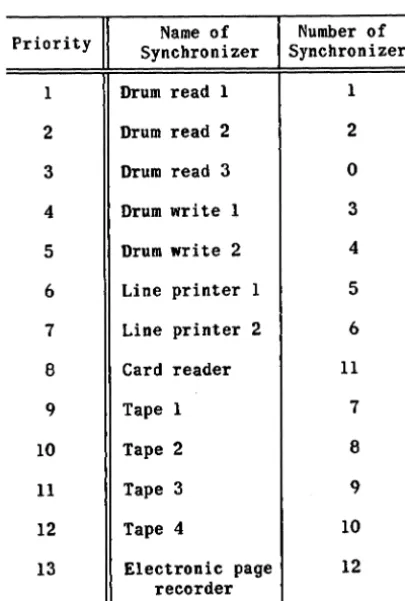
2·4. ORDER OF PRIORITY
The priority circuits assign the time slots to the synchronizers in the order of priority listed in table 2-1. Note, however, that the numerical designations of the synchronizers, of their signal names, and of the prior-ity circuits associated with them, are not an indication of priorprior-ity rating. The drum synchronizers have the highest priority rating because they oper-ate at the highest data-transfer roper-ate and are most susceptible to overflow and underflow. Although the line printers have an output rate which is less than that of the tape units, the printer synchronizers have higher priority because they contain only one output-buffer register each, as opposed to two each in the tape synchronizers. Further, since a line printer requires numerous references to the memory for every word printed, its synchronizer is therefore more susceptible to underflow than a tape synchronizer. The
..
Table 2-1. Order of Time-Slot Priority of Synchronizers
Priority Synchronizer Name of Synchronizer Number of
1 Drum read 1 1
2 Drum read 2 2
3 Drum read 3 0
4 Drum write 1 3
5 Drum write 2 4
6 Line printer 1 5
7 Line printer 2 6 8 Card reader 11
9 Tape 1 7
10 Tape 2 8
11 Tape 3 9
12 Tape 4 10
13 Electronic page 12 recorder
card reader has a comparatively high data-input rate per card, which places its synchronizer in a priority rating below the synchronizers of the line printers but above those of the tapes, even though the card-reader izer has two input-buffer registers. The electronic-page-recorder synchron-izer is last in order of priority because the recorder has the character-istic of not requiring information at a continuous rate.
The priority assignments among synchronizers of the same type are ar-bitrary.
2-5. SPECIAL UNDERFLOW PRECAUTIONS FOR DRUM WRITE SYNCHRONIZERS
The arbitrary assignment of priority among drum synchronizers might, under certain conditions, lead to underflow. since the drum write synchron-izers are assigned a lower priority, although they operate at the same data-transfer rate as the drum read synchronizers. The worst possible condition is one in which more than one drum synchronizer refers to the same memory unit. Under such a condition a low-priority drum write synchronizer near-ing underflow might not be able to achieve memory access in time because (1) its requests for a time slot might be overridden by requests from a drum synchronizer of higher priority, or (2) if it was allotted a time slot, the time slot might be wasted because the memory was busy with a read or write operation for a drum synchronizer of higher priority. To obviate such a situation, the priority circuits for the drum synchronizers are designed
in such a way that a drum write synchronizer of low priority nearing under-flow will override any drum synchronizer of higher priority for memory re-ference. Thus. if either drum write synchronizer 1 (S3) or 2 (S4) approach-esunderflow. it receives first priority; if both approach underflow. drum write synchronizer 2 (S4) receives first priority and 1 (S3) second.
2-6. OPERATION OF PRIORITY CIRCUITS
An operating synchronizer will require access to the memory (1) if it is an input synchronizer whose input-buffer register is filled with a word ready to be sent to the memory. or (2) if it is an output synchronizer whose output-buffer register is empty and ready for a new word from the memory.
Whenever memory access is required by synchronizer j.* a word-transfer-request FF in the synchronizer is set. The set output signal of this FF (SjRF) alerts the synchronizer-j priority circuit to begin competing with the priority circuits of all other operating synchronizers for the earliest time slot to which synchronizer j is entitled. The word-transfer-request FF will remain set until synchronizer j makes a successful memory reference;
it is reset by the signal SjRFR generated in the buffer-register control circuits when the memory-not-busy signal is received.
In the case of a fast-operating drum write synchronizer (S3 or S4). in which two output-buffer registers are used. the word-trans fer-request FF will be set as soon as one of the registers is empty. If the synchronizer still has not gained memory access for this register--that is. the word-transfer-request FF is still set---by the time a counter indicates that only eight digits remain in the other register. a nearing-underflow signal ~ or S40F is sent by the synchronizer to the priority circuits to insure that it receives first prior{ty.
Whenever the correct conditions prevail for synchronizer j to request memory access. the output signal of the set synchronizer-j word-transfer-request FF (SjRF) sets the syncbronizer-j priority-bid FF at T26 for a mini-mum of 2 ~s (figures 2-1 through 2-4). The output of this FF is gated with the outputs of the priority-bid FFs for the other synchronizers in such a way that signal PjA.B. indicating that priority is granted to synchronizer j. will be produced only if the priority-bid FFs of no other synchronizers of higher priority are set. While an address is bein~ransferred between an address register and register Pl. function signal 820 is present at the output gating of all priority-bid FFs to block all priority assignments.
When produced. priority signal PjA.B alerts circuits within the address-and buffer-register controls. address-and the address-modifier controls. These con-trols. at the correct time. set the address-modifier controls for synchron-izer j. read the address out of the synchronsynchron-izer-j address register. gate the address to the memory-address decoder. and write the same address back into the address register. The priority signal PjA.B is also delayed by the delayed-priority FF to produce delayed-priority signal PjD for 2 ~s. Signal PjD alerts the circuits in the address- and buffer-register controls; if the memory is not busy. these circuits will
*
j is any synchronizer.(1) Clear the old address out of the synchronizer-j address register;
(2) Write in the modified address;
and
(3) Write the new word coming from memory into the correct output-buffer register if synchronizer j is an output synchronizeri
or
(4) Read the word out of the correct input-buffer register for trans-mission to the memory if synchronizer j is an input synchronizer.
A signal SjMD derived from gating PjD with the MNB signal is used to indi-cate that priority for synchronizer j is no longer required and resets the synchronizer-j priority-bid FF. The SjRFR signal. which is similarly de-rived. resets the word-trans fer-request FF in the synchronizer.
2·7. AVOIDING TIME·SLOT WASTE
The SjMO signal. indicative of whether synchronizer j did or did not make a successful memory reference when a time slot was assigned to it. is returned to the synchronizer-j priority circuit after priority to the follow-ing time slot has already been assigned. Whether or not synchronizer j
makes a successful reference on the first time slot. the following time slot is given to the next calling synchronizer; it is not reserved for synchron-izer j to use if it failed to gain access on its first attempt. If the following time slot were reserved in this way and synchronizer j gained access on its first attempt. the reserved time slot would be wasted. If under normal conditions synchronizer j fails to gain memory access on its allocated time slot. it has to relinquish the following time slot to an-other calling synchronizer and then compete again for a time slot. Because of the delay in returning the SjMD signal. if synchronizer j happens to be the only synchronizer requesting a time slot, its priority circuits will assign it one more time slot after the one on which it made a successful memory reference. This extra time-slot assignment will be ineffective. however. since the SjMO signal is also used to inhibit the address control circuits from gating the address to the memory. thereby preventing the ini-tiation of the second memory reference. Since synchronizer j is the only synchronizer addressing the memory. this case cannot be considered as wast-ing a time slot.
~
There are. however. instances in which time slots will pass unused in order to insure that (1) all drum synchronizers requesting priority will achieve memory access before any synchronizer requesting prior'ity other than a drum synchronizer and (2) any drum write synchronizer nearing underflow will gain memory access before any other synchronizer requesting priority. The basic system of priority ratings will always give a drum write
priority circuits of the drum synchronizers are designed to operate in the following manner:
(1) If there are no other drum synchronizers requesting priority. the last requesting drum synchronizer receives as many successive time slots as may be necessary to gain memory access, plus an extra unused one, regardless of any outstanding priority demand by a synchronizer other than a drum syn-chronizer.
(2) If a drum write synchronizer is in the nearing-underflow state, it will receive highest priority and as many successive time slots as may be needed to gain memory access, plus an extra unused one. regardless of which other synchronizers have outstanding demands (drum write, drum read, or other). The one exception to this situation is when drum write synchron-izer 1 (53) is nearing underflow and drum write synchronsynchron-izer 2 (54) is re-questing priority in the normal way. In this event drum write synchronizer 1 (53) will receive the higher priority but must relinquish the next time slot to drum write synchronizer 2 (54) even though it (53) may not have gained memory access. Then, of course, whether drum write synchronizer 2 (54) gained memory access or not, priority will revert to drum write syn-chronizer I (53). If the demand of drum write synsyn-chronizer 2 (S4) is still outstanding when drum write synchronizer 1 (53) gains access, there will be no extra unused time slot.
(3) If both drum write synchronizers I and 2 (53 and 54) approach underflOW simultaneously, drum write synchronizer 2 (54) will immediately have the kind of priority described first in the preceding item (2), and drum write synchronizer I (53) will then assume precisely the same kind of priority after drum write synchronizer 2 (54) had gained memory access and the unused time slot has elapsed.
2·8.
CONDITIONS OF PRIORITYThe synchronizer is granted or refused priority under the conditions listed under headings 2-9 through 2-12. Refer to logical drawings 0807520 ••• 524. The signals representing the conditions are in parentheses. The letter j represents the designatory number of any synchronizer. and the
'ands' and 'ors' used between conditions are logical ANDs and ORs.
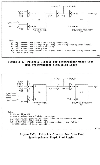
2-9. SYNCHRONIZER5 OTHER THAN DRUM 5YNCHRONIZERS
Figure 2-1 shows the priority circuit for synchronizers other than drum synchronizers.
Priority is granted to synchronizer j when the following conditions pre-vail:
(1) The synchronizer-j word-transfer-request FF is set (SjRF low);
and
and
(3) No higher priority demands are outstanding (PnF low·).
Priority for synchronizer j is refused when one of the following con-ditions occurs:
(1) A demand of higher priority arises (PnF high):
or
(2) A demand of lower priority arises (PmF high··), and synchronizer j was assigned priority on the preceding time slot (PjD high):
or
(3) Synchronizer j makes a successful memory reference (SjMD high).
2-10. DRUM READ SYNCHRONIZERS 1, 2, AND 3 (51, 52, SO)
Figure 2-2 shows the priority circuit for drum read synchronizers 1, 2, and 3 (51, 52, and 50).
Priority is granted to drum read synchronizer 1, 2, or 3 (51, 52, or SO) when the following conditions prevail:
(1) The synchronizer word-trans fer-request FF is set (51RF, 52RF, or SORF low);
and
(2) Underflow is not imminent on drum write synchronizers 1 or 2 (53 or 54) (530F. 540F low);
and
(3) The synchronizer was not granted priority to the preceding time slot (PlO. P2D. or POD low);
and
(4) A demand of higher priority is not outstanding (PlF low for drum read synchronizer 2 (52), PlF or P2F low for drum read synchronizer 3 (SO).
Priority for drum read synchronizer 1. 2. or 3 (51. 52. or 50) is re-fused when one of the following conditions arises:
(1) Underflow becomes imminent on drum write syncAronizers 1 or 2 (53 or 54) (S30F or S40F high):
*
n is any synchronizer of higher priority rating than j.**
m is any synchronizer of lower priority rating than j.SjMD
PI"T\F
Notes:
5
FF
R
PRIORITY BID
FF
PnF
Pj F PjA, B
5
FF
R
DELAYED PRIORITY
FF
j: Any synchronizer other than drum synchronizer.
n: Any synchronizer of higher priority (including drum synchronizers). m: Any synchronizer of lower priority.
5et pulse overrides reset pulse.
PjD
PjF is PmF for synchronizers of higher priority and PnF for synchronizers of lower priority.
Figure 2-1. Priority Circuit for Synchronizer Other than Drum Synchronizer: Simplified Logic
s S
PnF
.SjMD FF FF
S30F
S40F
PrnF R. R
PRIORITY BID DELAYED PRIORIT'I
FF FF
Notes:
j : 51 -0 r 52 0 r 50
n1 Any synchronizer of higher priority.
m: Any drum synchronizer of lower priority (including S3, 54). 5et pulse overrides reset pulse.
PjF is PmF for ~ynchronizers of higher priority and PnF for synchronizers of lower priority.
Figure 2-2. Priority Circuit for Drum Read Synchronizer: Simplified Logic
4776
PjD
54-Of
53MD
P4-F
53RF T26
54-OF
P3D
5
fF
R
PRIORITY BID
FF
P"F
FF
DEL A-(ED PRIORIT'l
FF
Notes:
n: Any synchronizer of higher priority. Set pulse overrides reset pulse.
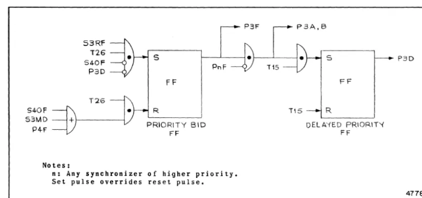
Figure 2-3. Priority Circuit for Drum Write Synchronizer I (S3): Simplified Logie
or
P3D
4778
~) The synchronizer makes a successful memory reference (SIMD, S2MD, or SOMD hig h);
or
(3)
A
demand of higher priority arises (PIF high for drum read syn-chronizer 2 (S2); PIF, P2F high for drum read synsyn-chronizer 3(SO»;
or
(4) The synchronizer was granted priority on the preceding time slot (PID, P2D, or POD high) and a demand of lower priority arises from a drum synchronizer (P2F. POF. P3F, or P4F high for drum read synchronizer 1 (Sl); POF. P3F or P4F high for drum read synchronizer 2 (52); P3F. or P4F high for drum read synchronizer 3 (SO».
2-11. DRUM WRITE SYNCHRONIZER 1 (S3)
Figure 2-3 shows the priority circuit for drum write synchronizer 1
(S3).
Priority is granted to drum write synchronizer I (S3) under the follow-ing conditions:
(I) The word-transfer-request FF of drum write synchronizer I (S3) is set (S3RF low);
and
(2) Drum write synchronizer I (S3) was hot granted priority on the preceding time slot (P3D low);
and
(3) Underflow on drum write synchronizer 2 (54) is not imminent (S40F low);
and
(4) No demands of higher priority are outstanding PlF, P2F and POF low).
Priority for drum write synchronizer 1 (53) is refused when
(1) Underflow on drum write synchronizer 2 (54) is imminent (S40F high) •
or
(2) Drum write synchronizer 1 <53) was granted priority on the pre-ceding time slot (P3D high) and a demand of lower priority arises from a drum synchronizer (P4F high).
or
(3) A demand of higher priority arises (PlF, P2F, or POF high);
or
(4) Drum write synchronizer 1 <53) makes a successful memory refer-ence (S3MD high).
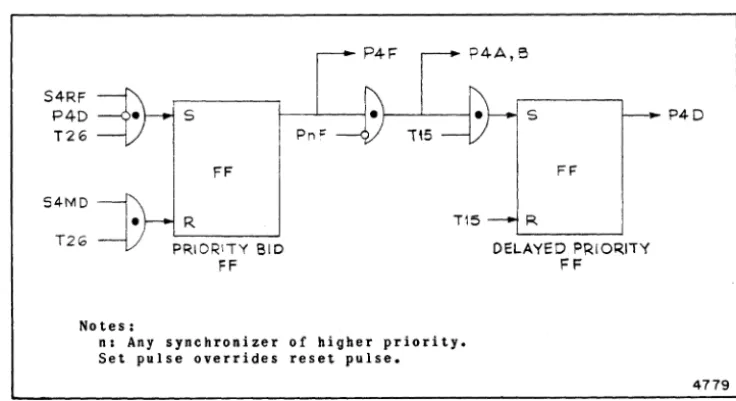
2-12. DRUM WRITE SYNCHRONIZER 2 (54)
Figure 2-4 shows the priority circuit for drum write synchronizer 2 (54) •
Priority is granted to drum write synchronizer 2 <54) when the follow-ing conditions prevail.
(1) The word-trans fer-request FF of drum write synchronizer 2 (54) is set (S4RF low);
and
(2) Drum write ~chronizer 2 (54) was not assigned priority to the preceding time slot (P4D low);
and
Priority for drum write synchronizer 2 (54) is refused when
(1) A demand of higher priority arises (PIF, P2F, POF, or P3F high);
or
(2) Drum write synchronizer 2 (54) makes a successful memory refer-ence (S4MD high).
S4RF
P4D S ~ P4D
T26
FF
541'11D
R
T2G
PRIORITY 810 FF
Pn"
FF
DELAYED PRIOR,ITY
FF
Notes:
n: Any synchronizer of higher priority. Set pulse overrides reset pulse.
Figure 2-4. Priority Circuit for Drum Write Synchronizer 2 (54): Simplified Logic
2-13. ORDER OF TIME-SLOT ASSIGNMENT: EXAMPLES
4779
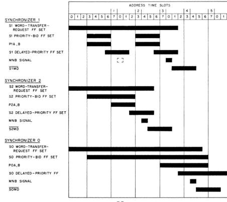
Figures 2-5 and 2-6 are timing diagrams chosen as examples of the se-quence in which calling synchronizers receive priority to the synchronizer time slots, depending upon various conditions such as whether the memory is busy when addressed or whether the priority circuits of the drum synchron-izers are able to insure that the drum synchronsynchron-izers will achieve first mem-ory access.
Figure 2-5 illustrates a competition for synchronizer time slots among drum read synchronizers I, 2. and 3 (51, 52, and SO). Since drum read syn-chronizer 1 (51) has the highest priority rating, it receives priority to the first time slot. The second time slot is allotted to drum read syn-chronizer
2
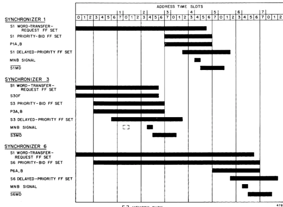
(52). In the meantime, however. drum read synchronizer 1 (51) has failed to gain memory access. and its priority request is therefore out-standing to override that of drum read synchronizer 3 (SO) for the third time slot. The fourth time slot then is assigned to drum read synchronizer 3 (SO), and. since by this time drum read synchronizer 3 (SO) is the only calling synchronizer. it also receives the fifth time slot, although it does not need it.The timing chart of figure 2-6 shows the competition for synchronizer time slots and for memory access between drum read synchronizer 1 <51), drum write synchronizer 1 (53) nearing underflow. and line-printer
SYNCHRONIZER 1 SI
WORD-TRANSFER-REQUEST FF SET SI PRIORITY-BID FF SET PIA ,B
S1 DELAYED-PRIORITY FF SET MNB SIGNAL
SIMD
SYNCHRON IZER 2 S2
WORD-TRANSFER-REQUEST FF SET S2 PRIORITY-BID FF SET P2A,B
S2 DELAYED-PRIORITY FF SET MNB SIGNAL
S2MD
SYNCHRONIZER 0 SO
WORD-TRANSFER-REQUEST FF SET SO PRIORITY- BID FF SET POA,B
SO DELAYED - PRIORITY FF MNB SIGNAL
SOMD
°l1123141.516
ADDRESS TIME SLOTS
I I 2 I 31 41 7 1011 12 31415j6 710-' 1 12 31 4 1 5 1 6
r- ,
•
'- oJ•
•
~ ~ MEMORY BUSY
Figure 2-5. Example of Time-Slot Assignment for Drum Read Synchronizers 1, 2, and 3 (51, 52, SO)
51 71 0 1 t 12
4780
izer 2 (56). Because drum write synchronizer 1 (53) is nearing underflow (530F) , it receives the highest priority and therefore the first time slot. To assure it of first memory access, it also receives the second time slot
SYNCHRONIZER 1
51 WORD-TRANSFER-REQUEST FF SET 51 PRIORITY- BID FF SET
P1A,B
51 DELAYED-PRIORITY FF SET
MNB SIGNAL
S1MD
SYNCHRONIZER 3
51 WORD-TRANSFER-REQUEST FF SET 530F
53 PRIORITY - BID FF SET
P3A,B
53 DELAYED- PRIORITY FF SET
MNB SIGNAL
S3MD
SYNCHRONIZER 6
011J 2 31 4J 5 16
ADDRESS TIME SLOTS
1 I 21 31 41 51
71 ° 11 12 31 4J5 16 7J01 11 2 31 4 15 16 71°j1j2
•
I I
,.... -,
•
L.~
S1
WORD-TRANSFER-REQUEST FF SET I L ~
56 PRIORITY-BID FF SET
I
P6A,B
~
56 DELAYED -PRIORITY FF SET
MNB SIGNAL
S6MD
[J MEMORY BUSY
Figure 2-6. Examples of Time-Slot Assignment for Drum Read Synchronizer 1 (51), Drum Write Synchronizer 1 (53),
and Line-Printer Synchronizer 2 (56)
61 71
31 4 1 5 16 71°1 1J2
•
SECTION III
ADDRESS AND BU FFER REGISTERS
3-1. GENERAL
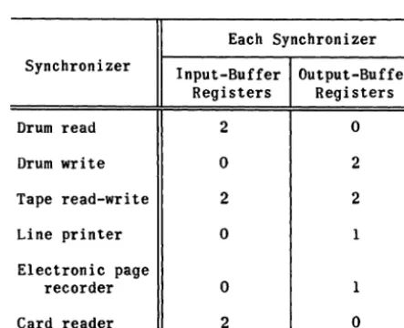
Within the dispatcher there is an address register for each synchron-izer in the system, two input-buffer registers for each input synchronsynchron-izer, and one or two output-buffer registers for each output synchronizer. Each address register is a five-digit register which stores the memory address of the next word to be transferred to or from the memory for a particular operating synchronizer. Each buffer register is a 12-digit register used as temporary storage for data in the process of being transferred between the memory and an input or output device controlled by a particular syn-chronizer. Table 3-1 lists the number and type of one-word buffer regis-ters required for each type of synchronizer.
3-2. BASIC CHARACTERISTICS
The address and buffer registers are composed of magnetic cores ar-ranged in separate address-register, input-buffer-register, and output-buffer-register matrices. The same circuit elements are used in all three matrices, although there is considerable difference in the overall config-urations of the matrices which reflects the differences in their function.
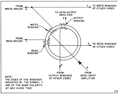
The basic circuit element of the register matrices is a fast-switch-ing tape-wound magnetic core (figure 3-1). Each core has three windfast-switch-ings-- windings--a write winding, windings--a rewindings--ad winding, windings--and windings--an output winding. The rewindings--ad windings--and write windings are driven, respectively, by magnetic-amplifier read and write drivers.
Reading or clearing a core requires a negative pulse from the read driver at point 1. This negative pulse will tend to switch the core to the cleared or
a
state. If a binary 1 is initially stored in the core, the read driver will switch the core to thea
state and produce a posi-tive output pulse representing a 1 at point 2. If, however, the core is initially in thea
state, the core will not be switched and point 2 will remain low, indicating aa
output.FROM __ - ... - - - . . : . . 7 _ TO WRITE WINDINGS
WRITE DRIVER 4 OF OTHER CORES
FROM
READ DRIVER
_---4
NOTE:
THE SIDES OF THE WINDINGS INDICATED BY THE SYMBOL • ARE OF THE SAME POLARITY AT ANY GIVEN TIME.
TO DA TA-OUTPUT AMPLIFIER
2 OUTPUT
WINDING
\-_ _ ~..__---H~-3-- TO READ WINDINGS OF OTHER CORES
5
FROM OUTPUT WINDINGS
OF OTHER CORES
FROM DATA-INPUT
AMPLIFIER
4782
Figure 3-1. Core Windings: Schematic
To write information into a core requires a negative pulse from the write driver at point 4. Whether or not the core switches depends on the data input at point 6. If the core is assumed to be initially in the cleared or 0 state. it'will switch to the 1 state only if a positive pulse (representing a 1) appears at point 6 coincident with the negative pulse from the write driver at point 4. If either point 4 is positive or point 6 is negative. the core will remain in the initial 0 state.
A magnetic-amplifier read or write driver is set by a l-~s negative pulse. When set. it generates a 0.5-~s negative clock pulse. The read-and write-driver clock pulses are 180 degrees out of phase with respect to each other. All the read magnetic amplifiers are driven by an A-phase clock. and all of the write magnetic amplifiers by a B-phase clock. except in the output-buffer registers. where the write magnetic amplifiers are driven by an A-phase clock. and the read magnetic amplifiers by a B-phase clock. Both clocks are synchronized with the pulseformer clock that re-times signals throughout the logical circuits.
3-3. ADDRESS-REGISTER MATRIX
the synchronizers in the system are contained within a 25 x n matrix of magnetic cores.t The address-register matrix is shown in simplified form in figure 3-2.
The matrix has 25 parallel input and output circuits corresponding to the 25 bits of the address. Output windings of corresponding cores of each register are connected in series with a transistor output amplifier. The write windings of corresponding cores of each register are connected by means of isolating diodes to a transistor input amplifier.
Table 3-1. Number and Type of Buffer Registers for Each Synchronizer
Each Synchronizer Synchronizer
Input-Buffer Output-Buffer Registers Registers Drum read 2 0 Drum write 0 2 Tape read-write 2 2 Line printer 0 1
Electronic page
recorder 0 1
Card reader 2 0
Each register has an A-phase magnetic-amplifier read driver which is set by a l-~s read signal from the address- and buffer-register control circuit to drive the 25 cores of the register when an address is being read out or when the cores of the register are being cleared. Each regis-ter also has a B-phase magnetic-amplifier write driver which drives the 25 cores of the register as an address is being written into the register. Unlike the buffer registers in which the read and write drivers are set independently of each other, an address-register write driver is always set by the output of the read driver.
Whenever the next address is ready to be written into address regis-ter j,* the address-regisregis-ter-j read driver is set by signal SjAR from the address- and buffer-registers control. The output of the read driver reads out or clears the address already in address register j (output signals SARI ••• 25), and sets the register write driver. The output of the write driver coincides with the arrival at the address-register-matrix input am-plifiers of the next address (input signals SMRl ••• 25), writing it into address register j.
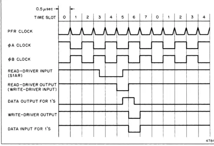
The timing for this read-write cycle is illustrated in figure 3-3.
t n represents the number of synchronizers in the system.
* j is any synchronizer in the system.
ADDRESS OUTPUTS TO OUTPUT PULSE FORMERS I SAR1 SAR2 SAR25 \
I--__tt--I---~-+---
-S1AR
I__ttI+...+r
-S2AR
REGISTERS 3 ... n-1
I--__tt--+---+-~-+--+--
-SnAR
LOGICAL SCHEMATIC SYMBOL REPRESENTATION
~=(t
, SMR1 SMR2 SMR25 , ADDRESS INPUTS FROM INPUT PULSEFORMERSFigure 3-2. Address-Register Matrix: Simplified Diagram
3-4. INPUT-BUFFER-REGISTER MATRIX
I I I I
I I
4783
An input-buffer register is a 60-bit magnetic-core register used by an input synchronizer as buffer storage for a word being transferred from an input device to the memory. (See figure 3-4 and logic drawings 0807560 ••• 563). Since the input device fills its input-buffer register one digit at a time, and a word sent over the memory HSB system is 60-bit parallel, the register is also designed to act as a series-to-parallel converter. A word is written into the register under control of the synchronizer and is read out by signals from the address- and buffer-register controls of the dispatcher.
Since all the input synchronizers operate at a comparatively high rate of data transfer, the time interval between words is not sufficient for successive words to gain access to the memory; consequently two one-word input-buffer registers are used alternately for each input synchronizer. While one word is being written into one register ('odd' registed, the
preceding word is waiting in the other register ('even' register) for the dispatcher to gain memory access for it. By the time the odd register is full, the word in the even register will have been sent to the memory. Then the roles of the registers are reversed. The terms 'odd' and 'even'
O.5J.Lsec
TIME SLOT
PFR CLOCK
¢A CLOCK
¢B CLOCK
READ-DRIVER INPUT (S1AR)
2 3 4 5 6
READ-DRIVER OUTPUT J--...,--I---+---+-~
(WRITE-DRIVER INPUT)
DATA OUTPUT FOR ,'S
J--...,--I---+--4--~
WRITE-DRIVER OUTPUT
DATA INPUT FOR 1'S
7 0 2 3 4
Figure 3-3. Timing of Read-Write Cycle of an Address Register
4784
Since a word is written into an input-buffer register with each par-allel-bit digit in series, the 60 cores of the register are connected in a 12 x 5 input matrix. The input-buffer registers for all the input syn-chronizers in the system are within a t x 60 matrix.*
Each register has 12 B-phase magnetic-amplifier write drivers, each of which energizes the write wi.ndings of the five cores in one digit posi-tion (figure 3-4). The write drivers are selected sequentially by a digit counter in the synchronizer, so that each digit of five parallel bits, fed to the register through five transistor amplifiers, will be stored in the five cores of the digit position specified by the sequential digit counter.
Because input to an input-buffer register is by one digit at a time, each successive digit should in theory be applied through the same five in-put amplifiers (one for each bit). The actual wiring of the registers, however, is such that 30 cores of the register are on one plane and the re-maining 30 on another; for this reason there are two sets of five input transistor amplifiers, one set for each half of the register. One set of input amplifiers is used for the first 30 cores of both the odd and even registers of one synchronizer; the other is used for the last 30 cores of both the odd and even registers. (See figure 3-4.)
Since the two registers of each synchronizer therefore have their own sets of input amplifiers and write drivers, the input circuits of the
reg-• t is the total number of input-buffer registers in the system.
isters of each synchronizer are independent of those of the registers of other synchronizers.
One complete word is read out of an input-buffer register at one time, all 60 bits in parallel. Each register has two A-phase magnetic-amplifier read drivers activated by a l-~s signal derived from the set state of the memory-ready FF in the address- and buffer-register control circuits. These amplifiers drive one half of the register each--that is, 30 cores--as illustrated in figure 3-4, but, since they are activated simultaneously, the contents of all 60 cores are read out in parallel through 60 transistor output amplifiers to the memory-write buffers. Only one set of 60 output amplifiers is provided for the 60 parallel-bit output of all t registers, since only one register can transfer information to the memory at anyone time. Thus, although each register has its own two read drivers, the cor-responding cores of all t registers have a common output path--that is, the output windings of all corresponding cores are connected in series.
Figure 3-4 illustrates the connections between the cores of two half registers, both odd and even, of drum read synchronizers 1 and 2 (51 and 52). The connections between the cores of the second halves of registers 1 and 2 are identical to those shown in figure 3-4. The cores representing digit positions 1, 2, and 6 are shown fully, but those representing digit positions 3, 4, and 5 are omitted for brevity.
The first six digits of a word of information transferred from it,s in-put device by drum read synchronizer 1 (51), for example, will be written into the first 30 cores of one of two input registers of the synchronizer in the following way.
Assume that the odd register for the synchronizer is already filled, and the synchronizer therefore specifies that the word to be transferred will go into the even register. When the first digit of the new word is fed through the five input amplifiers (lA) at the input to both the odd and even registers of the synchronizer, signal 5lWVl from the synchronizer activates the B-phase write driver controlling the first five cores of the even register. The first digit will therefore be written only into the first digit position of the even register. When the second digit is ap-plied to the same five input amplifiers, signal 5lWV2 will cause it to be written only into the second digit position of the even register, and so on until signal 5lWV12 writes the 12th digit into the 12th digit position of the even register (at the end of the second half of the register not shown in figure 3-4). Since the signals that activate the write drivers of an input register are derived from the digit counter within the syn-chronizer, the order in'which the digit positions in the register are fill-ed is dictatfill-ed by the ordei in which the digit counter of the synchronizer is stepped. Because of mode considerations, for example,a tape synchron-izer has several sequences for writing digits into its input-buffer regis-ter.
When the even register is filled with the word and the synchronizer has gained access to the memory, signal 51RV from the address- and buffer-register control activates two read drivers, one for each half buffer-register
(only one being shown, therefore), to read out the register content through the output amplifiers to the memory write buffers and onto the memory write H5B.
TO MEMORY WRITE BUFFERS (0807,512)
, - - - COMMON OUTPUT AMPLIFIERS - - - " SWI
t
I
OA 1HE TWO
T
HALF OF SY
REGISTERS NCHRONIZER 1
EVEN [
SIWVl <loB W 51 RV R
~
<loASlWDI <10:
,~~
<loASW2 SW3 SW4 SW5
t
+
1
1
I
OA 2 lOA 3 lOA4JlOA5~~
P'<~
P'<~
~'\
~~
~~
P'<~
~'\
1"\
IA IA IA
?
IA 51 51 51 51 51S1WV2 <loB W
SlWD2 <loB W
BIT 1 BIT 2 BIT 3 BIT4 BIT 5
T HALF OF SYN
HE TWO REGISTERS CHRONIZER 2 S2WVl <loB
EVEN [ S2RV W
R <loA 2WDI ¢B
S2WV2 <loB
4~
~~
K~
~'\
W~
S2WD2 ¢B
ooo~
~
¢A~
~
~
~
WIA
2
5
BIT 1
I A I A IA IA
52 52 52 52 BIT 2 BIT 3 BIT 4 BIT 5 DATA-I NPUT AMPLIFIERS
DIGIT 1
4:-SW6 SW7 SW8 SW9 SW10
t
t
t
t
t
lOA610A7
I
OA 8I
OA 9I
OA 10~~
~~ ~~
~~ ~'\
"\-~
~r\ ~r\ ~~
~'\
"t~
~~
~~
~~
Hr\
'\-~
~
~
rf\
~
-=.E="
DIGIT 2
, ,
,
, '\ J I J ~ ~ ~ ,~
I rDIGIT 3 ... 5
SW26 SW27 SW28 SW29 SW30
DIGIT 6
LOGICAL SYMBOL
WRITE IN DATA
4'7~TPUT
READ 1
OUT 3 DATA 5 6 INPUT SCHEMATIC REPRESENTATION
4795
Figure 3-4. Half Registers of Drum Read Synchronizers I and 2 (51, 52)
3-5. OUTPUT-BUFFER-REGISTER MATRIX
An output-buffer register is a 60-bit magnetic-core register used by a synchronizer as buffer storage for a word being transferred from the mem-ory to an output device. Such a word is sent from the memmem-ory on the HS8, all 60 bits in parallel, and is transferred to the output device one digit at a time; thus the output-buffer register is designed to act as a paral-lel-to-.series converter. (See figure 3-5 and logic drawings 0807564 ••• 567.)
The writing of a word into the output register is controlled by the address- and buffer-register controls of the dispatcher, and the reading out of a word by the synchronizer.
Where two output-buffer registers are used for one synchronizer, they are distinguished by the terms 'odd' and 'even,' as shown in figure 3-5.
Since a word is read out of an output-buffer register with each paral-lel-bit digit in series, the 60 cores of each register are arranged in a 12 x 5 output matrix. The output-buffer registers for all the output syn-chronizers in the system are within a t x 60 array.·
Each register has two A-phase magnetic-amplifier write drivers, each of which energizes the write windings of one half of the register, and 12 8-phase.magnetic-amplifier read drivers, one to energize the read windings of the five cores of each digit position in the register (figure 3-5).
For any output device except the line printer in an alphanumeric mode. a complete word of data from the memory is written into an output-buffer register, all 60 bits in parallel. Coincident with the arrival of the word. a signal from the address- and buffer-register controls energizes both of the write-amplifier drivers of the appropriate register to write the 60 bits in parallel into the 60 cores. Only one set of 60 input am-plifiers is provided as input to all the t registers. since only one regis-ter can receive information from the memory at anyone time. Thus. al-though each register has its own two write drivers. the corresponding cores of all the t registers have a common input path---that is. the data input windings of all corresponding cores are connected in series.
When an output device is ready to receive a word from its output-buf-fer register. sequential signals derived from a digit counter within the synchronizer set each of the 12 read amplifier drivers in turn to read out the 12 digits one after the other through a set of five output transistor amplifiers. As with input-buffer registers, the actual wiring of the out-put buffer registers is such that one set of five outout-put amplifiers is pro-vided for each half of each register (figure 3-5). Where a synchronizer has two registers, one set of output ampl.ifiers serves the same half of both the odd and even registers. The output path of the registers of each synchronizer is therefore independent of the output paths of the registers of other synchronizers.
The common 60-bit parallel input path to all registers is arranged on the logic drawings in this digit-position order, from left to right:
1 2 5 6 9 10 3 4 7 8 11 12
This digit-position order is dictated by the printout characteristics of the line printer in the alphanumeric mode. When operating in this mode, the line printer prints the three characters in digit positions I, 2, 5, 6, 9, and 10 of a word during one print cycle (figure 3-5), and then in a later print cycle prints the three characters in digit positions 3, 4, 7, 8, II, and 12. Because of these two separate print cycles required for the printing of one alphanumeric word, the line-printer output-buffer register is used as two separate 30-core registers, which are filled and emptied at different times. The first time that a word to be printed is sent from the memory, only the write driver for the first 30 cores is activated, so that the first 30 cores are filled with digits I, 2, 5, 6, 9, and 10 of the al-phanumeric word. These digits are read out serially to the line printer. When the word is sent again from the memory, only the write driver for the second 30 cores is activated, so that digits 3, 4, 7, 8, II, and 12 are written into the remaining cores and read out serially to the line printer.
The 60 cores of the line-printer output-buffer register are therefore arranged in this digit-position order:
1 2 5 6 9 10 3 4 7 8 11 12
5ince the data-input path to all output-buffer registers is common, the cores of all output registers are arranged in the same order. This irreg-ular digit-position order does not, however, affect the order in which digits are read out of the