Volume 2006, Article ID 32408, Pages1–12 DOI 10.1155/ASP/2006/32408
A Fully Automated Environment for Verification of
Virtual Prototypes
P. Belanovi´c, B. Knerr, M. Holzer, and M. Rupp
Institute of Communications and Radio Frequency Engineering, Vienna University of Technology, 1040 Vienna, Austria
Received 15 October 2004; Revised 29 March 2005; Accepted 25 May 2005
The extremely dynamic and competitive nature of the wireless communication systems market demands ever shorter times to market for new products. Virtual prototyping has emerged as one of the most promising techniques to offer the required time savings and resulting increases in design efficiency. A fully automated environment for development of virtual prototypes is pre-sented here, offering maximal efficiency gains, and supporting both design and verification flows, from the algorithmic model to the virtual prototype. The environment employs automated verification pattern refinement to achieve increased reuse in the design process, as well as increased quality by reducing human coding errors.
Copyright © 2006 P. Belanovi´c et al. This is an open access article distributed under the Creative Commons Attribution License, which permits unrestricted use, distribution, and reproduction in any medium, provided the original work is properly cited.
1. INTRODUCTION
Complexity of modern embedded systems, particularly in the wireless communications domain, grows at an astound-ing rate. This rate is so high that the algorithmic complex-ity now significantly outpaces the growth in complexcomplex-ity of underlying silicon implementations, which proceeds accord-ing to the famous Moore’s Law [1]. Furthermore, algorithmic complexity even more rapidly outpaces design productivity, expressed as the average number of transistors designed per staff/month [2,3]. In other words, current approaches to em-bedded system design are proving inadequate in the struggle to keep up with system complexity.
Hence, a number of new system design techniques with potential to speed up design productivity are intensively re-searched [4,5]. One of these techniques known as virtual prototyping [6–8] speeds up the design process by enabling development of hardware and software components of the embedded system in parallel.
Development of a comprehensive design environment for automatic generation and verification of virtual proto-types (VPs) from an algorithmic-level description of the sys-tem is presented here.Section 1.1describes the concept of a VP in closer detail andSection 1.2explains the model of the hardware platform used in this work. A survey of re-lated work, including a comparison of the presented environ-ment with the most advanced current approaches, is given in Section 1.3. The design environment for automatic genera-tion of VPs is described in detail in Section 2. The part of
the presented environment concerned with automated veri-fication pattern refinement for VPs is presented inSection 3, together with an example design. Finally, conclusions are drawn inSection 4.
1.1. Virtual prototype concept
System descriptions at algorithmic level contain no specific implementation details. Hence, before implementation of the system can begin, the algorithmic description is parti-tioned, that is, each component in the description is assigned to software or hardware implementation.
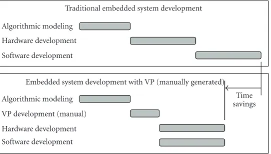
Traditionally, implementation of hardware components proceeds from this point. Development of software modules, however, can begin only once all required hardware design is complete. This is due to the fact that the design of software components must take into consideration the behaviour of the underlying hardware. Hence, a significant penalty is in-curred in the length of the design process (seeFigure 1, top chart).
Traditional embedded system development Algorithmic modeling
Hardware development Software development
Embedded system development with VP (manually generated) Time savings Algorithmic modeling
VP development (manual) Hardware development Software development
Figure1: Shortening of the design cycle by the VP technique.
The speedup in the system development cycle by employ-ing virtual prototypemploy-ing is achieved as depicted inFigure 2. Firstly, the algorithmic model is partitioned into components to be implemented in hardware and those to be implemented in software. This defines the hardware-software interfaces in the system. InFigure 2, blocks B, C, and E have been assigned to implementation in hardware and blocks A, D, and F in software. The algorithmic description is then remodeled to a form where these interfaces are clearly defined. Thus, the VP of the system is created.
From this point, hardware and software development proceed in parallel. It is important to note that all blocks as-signed to hardware implementation are grouped into a num-ber of VP components, each of which will later be realised as a separate hardware accelerator in the system architecture. In Figure 2, blocks B and C form the VP component 1, whereas block E alone forms the VP component 2.
Development of the hardware implementation of VP component 1 is done against the hardware-software inter-face defined in the VP. Similarly, the software implementa-tion of VP component 2 relies on the existence of the same hardware-software interface. At the same time, the develop-ment of the software impledevelop-mentation of VP component 3 makes use of the same interface. Such use of the VP en-sures co-operability of the three implementations, allowing for their parallel development and the resulting time savings. Virtual prototyping offers numerous improvements to the design process. First and foremost, it allows parallel de-velopment ofallcomponents in the system, resolving all in-terface dependencies. Furthermore, it allows verification of software components which interface with hardware against the known hardware-software interface. Finally, a VP allows verification of the hardware implementation itself, making sure the hardware indeed provides correct interface to ex-ternal components as it was designed for at the algorithmic level.
Very importantly, creation of a VP for a system com-ponent requires a relatively small design effort, compared to that of a full hardware or software implementation. This is due to the relaxed requirement of the VP to recreate
behaviour only at component boundaries, allowing all other implementation details to be overlooked. As seen inFigure 1 (bottom chart), this allows the time savings which make VP a desirable design technique.
1.2. Model of hardware platform
The structure of the hardware platform assumed in this work is a generic multiprocessor system-on-chip (SoC) ar-chitecture. At least one processor core, such as the StarCore DSP, for example, is present in the architecture, as shown in Figure 3. All the system components assigned to software im-plementation will be targeted to one of these processor cores. Also present in the system are a number of hardware accel-erator (HA) blocks. These contain custom silicon designs to provide accelerated processing for time-critical system func-tions. All the system components assigned to hardware im-plementation will be realised as these HA blocks. The system also contains one or more banks of system memory and a dedicated direct memory access (DMA) controller, serving the processor cores as well as the HA blocks.
Communications on this hardware platform are facili-tated by at least one system bus, such as an AMBA bus for ex-ample, connecting all system components. Additionally, HA blocks may be provided with dedicated direct I/O ports, for off-chip communications.
1.3. Related work
Hardware development
Virtual prototype Comp2
(HW) Comp1 (HW)
B C E
A D F
Algorithmic model
A B C
D E F
Comp1 Comp2
HW HW
A D F
B C E
Comp3
Comp1 Comp2
Comp3 Software
development Comp3 (SW)
HA1 HA2
DSP
SW
Final
implementation
Figure2: System development using a VP.
DMA DSP
HA1 HA2
Direct I/O
System bus
RAM
Figure3: Target hardware platform.
On the other hand, St¨ohr et al. [11] present FlexBench, a fully automated methodology for reuse of component-level stimuli in system verification. While this environment presents a novel structure which supports verification pat-tern reuse at various abstraction levels without the need for reformatting of the verification patterns themselves, this in turn creates the need for new “driver” and “monitor” blocks in the environment for every new component being verified. Also, this environment has only been applied to hardware components.
An automated testing framework offered by Odin Tech-nologies called Axe [12] also offers automated reuse of ver-ification patterns during system integration. However, this environment requires manual rewriting of test cases in Mi-crosoft Excel and relies on the use of a third-party test au-tomation tool on the back end. Also, the Axe framework has only been applied to development of software systems.
The verification extension of the virtual prototyping en-vironment presented here is also designed to provide fully
automated verification pattern refinement, but addresses this issue in a more general manner than previously published work. Hence, it is applicable to both software and hardware components, and indeed to verification pattern refinement between any two abstraction levels, though the particular instance of this framework presented here is specific to the transition from algorithmic to virtual prototype abstraction levels.
2. AUTOMATED VIRTUAL PROTOTYPE GENERATION
As described earlier, design of an embedded system proceeds from the algorithmic-level description towards the system’s final implementation firstly through a partitioning process, followed by the creation of a VP and finally hardware or soft-ware implementation of each individual component.
The process of VP generation is typically performed manually, through rewriting of the VP from the algorithmic-level description. However, when the VP design environment is integrated into a unified design methodology, it is possi-ble to make VP generation a fully automated process. This helps eliminate human errors and drastically decrease the time needed to create a VP, in turn deriving maximum possi-ble efficiency gain promised by virtual prototyping [13,14]. This is illustrated inFigure 4.
Embedded system development with VP (manually generated)
Algorithmic modeling VP development (manual) Hardware development Software development
Embedded system development with VP (automatically generated) Time savings Algorithmic modeling
VP development (automatic) Hardware development Software development
Figure4: Shortening of the design cycle by automating VP generation.
HW/SW partitioning information
table
COSSAP project
W X Z
Y Fileset
.gc v arc v ent
COSSAP guidelines
SDI for COSSAP
SSD VPG
VP components for W, X, Y, Z Bus interface
C A
B Scheduler
Figure5: Design environment for automatic generation of VPs.
2.1. Processing the algorithmic description
The environment for automatic generation of VPs presented here is based on processing algorithmic descriptions created in the COSSAP environment. Nevertheless, the VP environ-ment is in principle independent of languages and tools used for algorithmic modelling and can, due to its modular struc-ture, easily be adapted to any language or tool.
COSSAP descriptions contain separate structural/inter-connection and functional information. The structural and interconnection information in the COSSAP description is VHDL-compliant and is read into the SSD by the system description interface (SDI). The SDI comprises a VHDL-compliant parser module as well as a scanner module which manages the database structure within the SSD.
The functional information in COSSAP descriptions is written in GenericC (extension to ANSI C proprietary to the
COSSAP environment) and has to be formatted in accor-dance with specific guidelines. These guidelines ensure com-patibility of the GenericC code with tools in the second phase of the automatic VP generation. Suitably formatted func-tional component descriptions are placed directly into the SSD.
Initial concept
. . .
Leveln
Leveln+ 1 . . .
Final product
Model (leveln)
Model refinement
Model (leveln+ 1)
Verification
Refinement information
Verification
Verification patterns (leveln)
Verification pattern refinement
Verification patterns (leveln+ 1)
Figure6: Conceptual view of parallel refinement of the model and the associated verification patterns.
2.2. Virtual prototype generation
A VP component is composed of several parts, as shown in Figure 5. The core of the VP component is the recreated in-terconnected block structure, as found in the algorithmic-level model—blocks A, B, and C in Figure 5. Additionally, the VP component contains a scheduler which controls the execution of each block, according to the current input and output sample rates of each block and the availability of data to be processed. Finally, the VP component contains a bus interface, responsible for communications between the VP component and the processor core(s) in the system over the bus. This block is shown in gray inFigure 5, because it needs to be created manually, depending on the bus type, commu-nications protocol, and processor core(s) used in the system. The second phase of automatic VP generation is per-formed by the virtual prototype generator (VPG) tool. This tool extracts all necessary structural information for the par-ticular component from the SSD and creates the intercon-nected block structure accordingly. Relevant functional in-formation in the SSD is code-styled to be compliant with the VSIA standard [16] and the C++ language and is then in-tegrated into the VP component. Following these steps, the automatically created VP component can be manually cus-tomised to a particular system bus, processor core(s), and communications protocols, before being used.
3. AUTOMATED VERIFICATION PATTERN REFINEMENT
As stated previously, design flows for embedded systems tra-ditionally start from initial concepts of system functionality, progressing through a number of refinement steps, eventu-ally resulting in the final product, containing all the software and hardware components that make up the system. These
refinement levels of a particular design flow may include the algorithmic level, architectural level, register transfer level (RTL), and others.
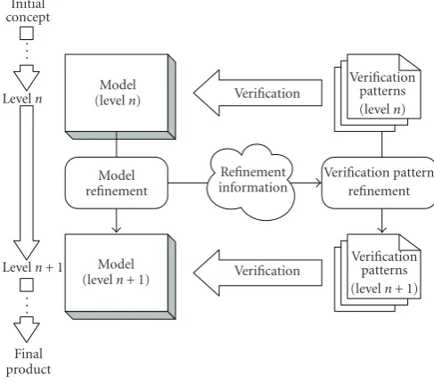
As the model of the design progresses from one refine-ment level to another, it needs to be verified for correct func-tionality at each level. Hence, the model of the system at each refinement level has associated with it a set of verification patterns, designed to verify correct functionality of the cor-responding model.
The verification patterns at each new level in the design flow are traditionally created from the verification patterns at the previous refinement level. This is shown inFigure 6. We refer to this process henceforth asverification pattern
refine-ment.
Whereas a great multitude of EDA tools and reseach work exists for automating refinement of system models between all the various refinement levels, there is a distinct lack of such support for verification pattern refinement. This causes both significantly prolonged verification cycles as well as lower design quality, due to the introduction of manual cod-ing errors. Hence, significant reduction of the time to mar-ket as well as improvement in quality can be achieved by au-tomating verification pattern refinement.
The manual process of verification pattern refinement, as it is customary in modern engineering practice, involves rewriting of the verification patterns from the earlier refine-ment level, applying the refinerefine-ment information which re-sulted from model refinement, to produce the new verifica-tion patterns (seeFigure 6). Hence, two distinct tasks can be recognised in the process of verification pattern refinement.
(i) Reformattingof verification pattern data, to fit the new
format required at the next refinement level.
(ii) Enrichmentof the same data, with the refinement
Algorithmic level verification patterns
Data-in streams
Data-out streams
Parameter-in stream
Parameter-out stream
Test generator
script
Interface specification
Direct I/O data
Memory
image Verificationprogram
Virtual prototype level verification patterns
Figure7: Structure of the environment for automatic generation of verification patterns.
original verification patterns, but is a necessary com-ponent in the newly created verification patterns.
Although the reformatting task can be, and frequently is, fully automated, current approaches to verification pattern refinement require manual effort from the designer in order to complete the enrichment task, for which traditionally no formal framework exists.
The environment for automated generation of vir-tual prototypes from algorithmic-level models presented in Section 2 demonstrated automated model refinement be-tween these two refinement levels. This section presents an environment for automating the corresponding verification pattern refinement, from the algorithmic level to the virtual prototype level, performing both reformatting and enrich-ment of the verification patterns automatically.
3.1. Verification at algorithmic level
At the algorithmic level, the model of the system contains no architectural information and the partitioning of the system is done on a purely functional basis. Hence, the model of the system typically assumes the form of a process network, with all functional blocks that make up the system executing con-currently and communicating through FIFO channels. Pop-ular commercially available environments for development and simulation of such models are Matlab/Simulink, COS-SAP, and SPW, among others. The work described here con-centrates on algorithmic models developed in the COSSAP environment, though with no substantial changes, it is appli-cable to other algorithmic-level models as well.
The presence of two types of information flowing through the FIFO communications channels of the model is assumed. The first type of information consists of parame-ters, responsible for controlling the modes of operation of each process. The second type of information isdata, the ac-tual values which are processed in the system and have no influence on the mode of operation of any process.
Therefore, verification patterns at the algorithmic level consist of a set of sequences of values, or streams. Exactly
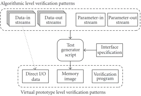
one stream exists for each of the data channels going into the model and one for each data channel going out of the model. A pair of dedicated parameter streams, exactly one for all parameters going into the model, and exactly one for those going out of the model, also exist. The complete set of streams is shown as algorithmic-level verification patterns in Figure 7.
Since no architectural or implementation information is yet known at the algorithmic level, the simulation of the model (and hence its verification) at this level is purely un-timed functional. In other words, the simulation is driven solely by the availability of input parameters and data, and their processing by the system modules.
3.2. Verification at virtual prototype level
Use of a virtual prototype implies a highly heterogeneous system. Initially, all of the components in the system have a general, purely algorithmic description. During parallel soft-ware and hardsoft-ware development of the various system com-ponents (see Figure 2), some of the initial component scriptions may be replaced by implementation specific de-scriptions. For hardware components these may be VHDL or Verilog descriptions, while for software components these may be written in Java or C++, for example. Hence, as the development of the system progresses, the VP becomes in-creasingly heterogeneous.
In this work, we focus on verification of system compo-nents assigned to hardware implementation, since they will be implemented as part of an HA block (seeFigure 3). Ver-ification of software components is entirely analogous, but has reduced complexity, because no HA blocks are involved (a more homogeneous problem).
Hence, verification at the virtual prototype level requires the following:
(i) device under verification (DUV), (ii) verification patterns,
Header Header Header
Input memory
image
output memory
image
Block 1 Block 2 Block 3
. . .
Blocki
Sequence 1 Sequence 2 Sequence 3
. . .
Sequencej
Values
Masks
Figure8: Structure of the memory image.
It is important to note that the structure of the hardware platform (seeFigure 3) enforces the separation of verification patterns into two types, according to how they are commu-nicated to the DUV. Hence, there exist verification patterns communicated to the VP through the system bus (stored in a structured memory image) and those communicated to the VP through its direct I/O interfaces (supplied directly to the VP during functional simulation). Both of these types of ver-ification patterns are shown as virtual prototype-level verifi-cation patterns inFigure 7, together with the necessary veri-fication program.
Since verification at the virtual prototype level relies heavily on transactions over the system bus, it is imple-mented in a bus-cycle true manner. The bus interface of the DUV, as well as the rest of the simulation environment, in-cluding the VSIA-compliant models of the DSP and the sys-tem bus, are also accurate to this time resolution within the functional simulation of the complete system.
3.3. Environment for automatic generation of verification patterns
The environment for automated verification pattern refine-ment presented here generates virtual prototype-level verifi-cation patterns from algorithmic-level verifiverifi-cation patterns, as shown inFigure 7.
3.3.1. COSSAP verification patterns
The environment for algorithmic-level modelling consid-ered in this work is COSSAP from Synopsys. Hence, the algorithmic-level verification patterns used also come from the COSSAP environment. As seen inFigure 7, they are di-vided into four sets of streams parameter in and out, and data in and out streams.
Exactly one stream exists for all parameters supplied to the DUV during functional verification, as well as exactly one stream for all parameters read from the DUV. Exactly one stream exists for each data input port of the DUV and exactly one for each of its output ports.
The structure of each stream is a sequence of values to be supplied to the inputs or expected at the outputs of the DUV. Remembering that verification at the algorithmic level
follows an untimed functional paradigm, that is, is driven purely by the availability of input parameters and data, no further timing information needs to be contained in the streams.
3.3.2. Verification program
The verification program runs on the processor core and communicates with the DUV over the system bus. Its func-tion is to supply the appropriate verificafunc-tion patterns from the memory image to the DUV, as well as to verify the pro-cessing results of the DUV against the expected results, also stored in the memory image. The cycle of writing to/reading from the DUV is repeated for the complete set of verifica-tion patterns, on the basis of one input block and one output block being processed per cycle (seeSection 3.3.3for more details).
Functionality of the verification program is hence not de-pendent on the particular VP being verified. Thus, the veri-fication program is generic in nature, and can be reused for verification of any VP component. However, a separate ver-ification program must of course be written for every new processor core used in the system and being employed to run the verification of any DUV.
3.3.3. Memory image
The memory image is a structured representation of the ver-ification patterns for the virtual prototype level. It includes only those verification patterns which are to be supplied to or read from the DUV over the system bus.
As already mentioned, since the verification program is generic and applicable to the verification of any VP com-ponent, all verification pattern values, their sequence, and the appropriate interface information must be contained in the memory image. This in turn dictates the structure of the memory image: it contains all the above information, while both making it efficiently accessible in a generic manner by the verification program, as well as minimizing the memory size overhead required to establish this structure.
As a consequence, the memory image is organised as shown inFigure 8. It is primarily divided into theinput
mem-ory imageand theoutput memory image. The former contains
all verification patterns (both parameter and data) which are written to the DUV. The latter contains those verification patterns which are used to check the validity of the outputs of the DUV.
Further, each of the two primary parts of the memory im-age contains a header, followed by severalblocks. The header contains the number of blocks in the particular image, fol-lowed by a pointer to the beginning of each block, as well as a pointer to the end address of the last block. The latter pointer is effectively the pointer to the end of the particular image and is used in assessing the total size of the memory image by the verification program.
vc1 di1 pi1 di2 di3 di3
b1 b2
p1
d1 do1
po1 po2
System bus
di1 di2 di3 do1 di4 pin pout vc1
Direct I/O
Figure9: Model refinement of the virtual component vc1, from algorithmic level (left) to virtual prototype level (right).
by the DUV in a single functional invocation. Similar to the structure of the memory image itself, each block contains a header, followed by a number ofsequences. The header con-tains the number of sequences in the particular block, fol-lowed by a pointer to the beginning of each sequence.
A sequence is a set of verification pattern values to be written to or read from a contiguous section of the DUV’s register space. It is composed of a header, a set of values, and a set of masks. The header contains only the start ad-dress within the DUV’s register space where the write or read operation is to take place.
In the case of the input memory image, the values in a sequence are to be written to the DUV, while the masks de-termine which bits of each value are to be written to the DUV (overwriting the current content) and which bits are to be kept at their current state. Hence, the required oper-ation for writing the verificoper-ation patterns from the mem-ory image to the DUV is given (on the bit level) as n = ( ¯m·c) + (m·v), or a simple 1-bit multiplex operation, where
vis the value in the verification pattern,mis the mask,cis the current value in the DUV register space, andnis the new value.
In the case of the output memory image, the values in a sequence are to be compared to those returned by the DUV, to verify its functionality. The mask values are used to indi-cate which of the bits are to be verified and which bits can be regarded as “do not care.” Hence, the required operation while verifying the functionality of the DUV is given (on the bit level) ast=m·(c⊕v), wherevis the expected value,m is the mask,cis the current value in the DUV register space, andtis the test output. A failed test is indicated with the log-ical state “1” of the variablet.
3.3.4. Direct I/O data
As already mentioned inSection 3.2, during the verification process, some verification patterns are supplied to the DUV directly through the I/O interfaces of the HA (seeFigure 3) and not through the system bus. Hence, during the verifica-tion process these values are not handled by the processor core and are thus not part of the memory image.
The direct I/O data is therefore handled separately during the simulation process. A dedicated module in the simulation environment has been created to serve the sole purpose of making the direct I/O data available to the DUV through its direct I/O ports.
3.3.5. Interface specification
The interface specification (see Figure 7) contains all the structural information which is present, and naturally re-quired during verification, at the VP level, but did not ex-ist at the algorithmic level. Indeed, this interface information comes as a result of the refinement process, going from the algorithmic model to the VP.
In other words, the interface specification is the
refine-ment information(as depicted inFigure 6) between the
algo-rithmic level and the VP level. Hence, the interface informa-tion is needed in order to perform verificainforma-tion pattern refine-ment between these two levels.
The interface specification can contain interface informa-tion for several VP components. Each part dedicated to a par-ticular VP component is composed of exactly one parameter and one data section. The parameter section contains inter-face information for all the parameters of the VP component in question. Correspondingly, the data section contains in-terface specifications for each data channel (input as well as output) of the VP component in question.
The parameter interface information includes names of all parameters in the model, together with their bit-exact ad-dresses in the register space of the DUV. Unlike parameters, data is packaged for communication over the system bus and writing into the register space of the DUV. That is to say, several data values may be packaged into one register of the DUV. If the latter is 32 bits wide, it is efficient to package four 8-bit data values into a single register. Hence, the data section of the interface specification contains in addition to the name of the data input or output, also its packaging fac-tor (being four in the example above) and its starting address in the register space of the DUV.
3.3.6. Test generator script
The test generator script (TGS) lies at the core of the auto-mated environment for verification pattern refinement pre-sented here, as shown inFigure 7. Its main function is to cre-ate the VP level verification patterns, that is, perform both steps in the verification pattern refinement process automat-ically (seeSection 3).
di1 di1
di1 di1
di2 di2 di2 di2 di3
di3
pi1 do1 do1 do1 do1
po2 po1 01A0
01A1 01A2 01A3 01A4 01A5 01A6 01A7
Figure10: Register mapping of each data and parameter port of vc1.
Interface specification · · · Component vc1 Parameter Pi1 01A5 3 0 Po1 01A7 0 0 Po2 01A7 8 1 Data di1 bus 01A0 2 di2 bus 01A2 4 di3 bus 01A3 1 di4 IO do1 bus 01A6 4
Component vc2 · · ·
Figure11: Interface specification for the virtual component vc1.
the algorithmic verification patterns, followed by the analysis of the resulting single stream of patterns. As a result of this analysis, the structure of the memory image, with associated block, sequence, and pointer structures can be created.
The second step in the verification pattern refinement process is the enrichment of the verification patterns with re-finement information, that is, architectural details. This task achieves the filling out of the empty memory image struc-ture with the actual verification pattern values, with correct bus interface formats, including appropriate register map-ping. Hence, in order to complete this task, the TGS con-structs each sequence of each block, both in the input and the output memory image, by bitwise combination of the algo-rithmic verification patterns, according to the register map-ping found in the interface specification. Also, the TGS cre-ates the appropriate bitwise masks found in each sequence, again from the information found in the interface specifica-tion.
di1 New block CD9A 501C E0D5 4F05 New block 1AC1 7000
· · ·
di2 New block 1B 89 60 A1 New block 7B 70
· · ·
di3 New block 000B0855 002C4002 New block 00F4128E 00C11032 · · ·
do1 New block 22 01 84 74 New block 01 76
· · ·
para in New block pi1A New block New block pi1 3 New block
· · ·
para out New block po1 0 po2 04 New block po2 03 New block New block po2 1A
· · ·
Figure12: The COSSAP verification patterns for each port of vc1.
The so-prepared memory image is written by the TGS in binary file format, ready to be loaded directly into system memory, either within the VP simulation environment or (in the implementation stage of the design process) on the hard-ware platform itself.
3.4. Example design
An example design, showing the automated refinement of verification patterns for a virtual component vc1, from the algorithmic level to the virtual prototype level, is given in this section. Initially, this component undergoes refinement of the model itself, as shown inFigure 9. Here the model of vc1 in the algorithmic modelling environment, such as COS-SAP, is shown on the left. The component is made up of two subblocks, b1 and b2, connected by various data channels (represented by full lines, such as d1) and parameter chan-nels (represented by broken lines, such as p1).
On the right inFigure 9, the virtual prototype model of vc1 is shown. This model contains the same interconnected structure as that in the algorithmic model, butadditionally
it contains architectural information. This additional archi-tectural information is hence introduced into the model as a result of the refinement process, as shown inFigure 6as “Re-finement Information.” This architectural information in-cludes the architectural location of data ports, such as the assignment of input port di1 to the system bus interface and input port di4 to the direct I/O interface.
Moreover, this refinement information includes the reg-ister mapping of all data and parameter channels which have been assigned to the system bus interface, as described earlier in this section. The register mapping for the virtual compo-nent vc1 is shown inFigure 10. Hence, the bus interface be-tween the component vc1 and the processor core on which the software components are running occupies the section of the register space between addresses 01A0 and 01A7 (inclu-sive). Data corresponding to the input data port di1 occu-pies registers 01A0 and 01A1, with a packaging factor two (as described earlier). Similarly, the output parameters po1 and po2 occupy nonoverlapping (but bordering) sections of the register 01A7.
00 00 00 05 00 00 00 07
00 00 00 43 00 00 00 52 00 00 00 01 00 00 00 09 00 00 01 A0 50 1C CD 9A 4F 05 E0 D5 A1 60 89 15 00 0B 08 55 00 2C 40 02 00 00 00 0A FF FF FF FF FF FF FF FF FF FF FF FF FF FF FF FF FF FF FF FF 00 00 00 0F
00 00 00 05 00 00 00 5A
00 00 00 70 00 00 00 75 00 00 00 01 00 00 00 5C 00 00 00 A6 74 84 01 22 00 00 00 08 FF FF FF FF 00 00 01 FF
Number of blocks in the input image Pointer to input block 1
Pointer to input block 5 Pointer to end of input block 5 Number of sequences in input block 1 Pointer to sequence 1
Pointer to the starting address in the register space
Values
Masks
Number of blocks in the output image Pointer to output block 1
Pointer to output block 5 Pointer to end of output block 5 Number of sequences in output block1 Pointer to sequence 1
Pointer to the starting address in the register space Values
Masks Input image
header
00 01
05 06 07 08 09 0A 0B 0C 0D 0E 0F 10 11 12 13 14 15 16
52 53 54
58 59 5A 5B 5C 5D 5E 5F 60 61
75 Input block 1
Start of input block 2 End of input
block 5
Output image header
Output block 1
Start of output block 2 End of output
block 5
Input
image
Output
image
Figure13: The structure and content of the memory image for the virtual component vc1.
parameter pi1 will be read by vc1 from the address 01A5, occupying a total of four bits, between bits 0 and 3 inclu-sive. Similar specifications are given for the other parameters. The interface of each data channel is similarly described. For example, data associated with the output data channel do1 is to be written by the component vc1 to the system bus inter-face, at address 01A6, packaging four data values into each 32-bit register.
After the refinement information has been formally spec-ified, in the form of the interface specification, it is possi-ble to automatically generate virtual prototype verification patterns from algorithmic-level verification patterns. These algorithmic-level patterns are shown in Figure 12. As de-scribed earlier, each data input and data output port in the al-gorithmic model has associated with it a stream of values, in addition to the two dedicated parameter streams, para in and para out, for the input and output parameters, respectively.
Values in each stream are devided into blocks, for synchro-nization across streams.
As already explained, the idea of automated verification pattern refinement revolves around the enrichment of the algorithmic-level patterns with the refinement information that results from the model refinement, to create virtual pro-totype patterns automatically. The result is a memory image, containing the original algorithmic patterns, which are not only reformatted to fit the VP simulation environment (as well as the final hardware platform), but also appropriately enriched with the necessary architectural information, which is not present in the original verification patterns. The struc-ture and content of the memory image for the example vir-tual component vc1 is shown inFigure 13.
followed by a number of blocks. In this case, both images contain five blocks. Each block is composed of a header, fol-lowed by a number of sequences. In this example, both the first blocks of the input and the output image are shown fully, and both of them contain one sequence each.
Each sequence starts with a pointer to the starting address in the register space, where the reading (in the case of the input image) or writing (output image) is to start. Following this pointer, the rest of the sequence is made up of actual values and the corresponding masks, as described earlier. In this example, as can be seen inFigure 13, the first sequence of the first block of the input image is six values long, whereas the same in the output image is two values long.
4. CONCLUSIONS
In the rapidly changing and highly competitive field of wire-less communication systems, minimizing time to market is a key requirement for any commercially viable product devel-opment. While virtual prototyping has proved to be one of the most effective techniques for achieving the required time savings, it is only with full automation that the maximal gains can be achieved.
The presented environment for automated development of virtual prototypes not only offers these maximal time gains, but also supports the virtual prototyping process com-prehensively, in both the design and verification flows. In other words, the transition from the algorithmic-level to the corresponding virtual prototype is covered seamlessly by the presented environment, for both the model itself, as well as for the associated verification patterns.
The application of the presented environment is limited in its general applicability in several aspects. Firstly, the al-gorithmic descriptions considered in this work come from the COSSAP environment. While system descriptions origi-nating in any of the numerous other environments for algo-rithmic modelling have not yet been considered, the modular nature of the presented environment offers the possibility to process these other types of descriptions as well with minimal modifications and/or extensions. In particular, processing al-gorithmic descriptions in SystemC is being considered as a future extension to the presented environment, due to the strong presence of SystemC in the EDA market [17–19]. This will require only minimal extension to the presented envi-ronment, due to the already present ability of the underlying framework to process algorithmic descriptions in SystemC.
Furthermore, the verification strategy presented here has been implemented only for systems built around the Star-Core DSP [20]. However, the modular nature of the verifi-cation environment ensures the applicability of the environ-ment to systems build both around other processor cores as well as multiprocessor systems, with only minimal modifi-cations and/or extensions. One of the directions of future work being considered includes extending the environment to systems using other processor cores, by creating verifica-tion programs for a set of supported cores. This may also re-quire reformatting the associated memory images, to accom-modate varying register and memory widths. However, since
these widths are parameters in the TGS, no further modifica-tion to this script itself is required in order to adopt it to any set of processor cores.
ACKNOWLEDGMENTS
The authors would like to acknowledge the ongoing co-operation with Infineon Technologies and in particular thank Guillaume Sauzon, Thomas Herndl, Ahmad Sarashgi, Wolfgang Haas, and Johann Glaser for their collabora-tion. This work has been funded by the Christian Doppler Laboratory for Design Methodology of Signal Processing Al-gorithms.
REFERENCES
[1] G. E. Moore, “Cramming more components onto integrated circuits,” Electronics Magazine, vol. 38, no. 8, pp. 114–117, 1965.
[2] R. Subramanian, “Shannon vs Moore: driving the evolution of signal processing platforms in wireless communications,” in Proc. IEEE Workshop on Signal Processing Systems (SIPS ’02), pp. 2–2, San Diego, Calif, USA, October 2002.
[3] International SEMATECH, The International Technology Roadmap for Semiconductors, Austin, Tex, USA, 1999. [4] G. Karsai, J. Sztipanovits, A. Ledeczi, and T. Bapty,
“Model-integrated development of embedded software,” Proc. IEEE, vol. 91, no. 1, pp. 145–164, 2003.
[5] P. Belanovi´c, M. Holzer, D. Miˇcuˇs´ık, and M. Rupp, “Design methodology of signal processing algorithms in wireless systems,” inProc. International Conference on Com-puter, Communication and Control Technologies (CCCT ’03), pp. 288–291, Orlando, Fla, USA, July–August 2003.
[6] A. Hemani, A. K. Deb, J. Oberg, A. Postula, D. Lindqvist, and B. Fjellborg, “System level virtual prototyping of DSP SOCs using grammar based approach,”Design Automation for Em-bedded Systems, vol. 5, no. 3-4, pp. 295–311, 2000.
[7] C. A. Valderrama, A. Changuel, and A. A. Jerraya, “Virtual prototyping for modular and flexible hardware-software sys-tems,”Design Automation for Embedded Systems, vol. 2, no. 3-4, pp. 267–282, 1997.
[8] N. S. Voros, L. S´anchez, A. Alonso, A. N. Birbas, M. Bir-bas, and A. Jerraya, “Hardware-software co-design of complex embedded systems: an approach using efficient process mod-els, multiple formalism specification and validation via co-simulation,”Design Automation for Embedded Systems, vol. 8, no. 1, pp. 5–49, 2003.
[9] R. Ernst, “Codesign of embedded systems: status and trends,” IEEE Des. Test. Comput., vol. 15, no. 2, pp. 45–54, 1998. [10] P. Varma and S. Bhatia, “A structured test re-use
methodol-ogy for core-based system chips,” inProc. IEEE International Test Conference (ITC ’98), pp. 294–302, Washington, DC, USA, October 1998.
[11] B. St¨ohr, M. Simmons, and J. Geishauser, “FlexBench: reuse of verification IP to increase productivity,” inProc. Design, Au-tomation and Test in Europe Conference and Exposition (DATE ’02), pp. 1131–1131, Paris, France, March 2002.
[12] Odin Technology,Axe Automated Testing Framework, 2004,
www.odin.co.uk/downloads/AxeFlyer.pdf.
[14] P. Belanovi´c, B. Knerr, M. Holzer, G. Sauzon, and M. Rupp, “A consistent design methodology for wireless embedded sys-tems,”EURASIP Journal on Applied Signal Processing, Special issue on DSP enabled radio, 2005
[15] B. Knerr, M. Holzer, and M. Rupp, “HW/SW partitioning us-ing high level metrics,” inProc. International Conference on Computer, Communication and Control Technologies (CCCT ’04), Austin, Tex, USA, August 2004.
[16] U. Bortfeld and C. Mielenz, “White paper C++ System Simu-lation Interfaces,” Infineon, Munich, Germany, July 2000. [17] The Open SystemC Initiative (OSCI), San Jose, Calif, USA,
www.systemc.org.
[18] CoWare Incorporation, “SoC Platform-Based Design Using ConvergenSC/SystemC,” July 2002,www.coware.com. [19] T. Gr¨otker, S. Liao, G. Martin, and S. Swan,System Design with
SystemC, Kluwer Academic, Boston, Mass, USA, 2002. [20] StarCore DSP,www.starcore-dsp.com.
P. Belanovi´creceived his Dr. tech. degree in 2006 from the Vienna University of Tech-nology, Austria, where his research focused on design methodologies for embedded sys-tems in wireless communications, virtual prototyping, and automated floating-point to fixed-point conversion. He received his M.S. and B.E. degrees from Northeastern University, Boston, and the University of Auckland, New Zealand, in 2002 and 2000,
respectively. His research focused on the acceleration of image processing algorithms with reconfigurable platforms, both in re-mote sensing and biomedical domains, as well as custom-format floating-point arithmetic. Currently he is a Ph.D. candidate at the Vienna University of Technology, Austria, focusing on the design methodologies for embedded systems in wireless communications, virtual prototyping, and automated floating-point to fixed-point conversion.
B. Knerr studied communications engi-neering at the University of Saarland and the Technical University of Hamburg, Har-burg, respectively. He finished the diploma thesis about OFDM communications sys-tems and graduated with honours in 2002. He worked for one year as a Software Engi-neer for the UZR GmbH & Co KG, Ham-burg, on image processing and 3D com-puter vision. In June 2003 he joined the
Christian Doppler Laboratory for Design Methodology of Signal Processing Algorithms at the Vienna Technical University as a Ph.D. candidate. His research interests are hw/sw partitioning, multicore task scheduling, static code analysis, and platform-based design.
M. Holzerreceived his Dipl. Ing. degree in electrical engineering from the Vienna Uni-versity of Technology, Austria in 1999. Dur-ing his diploma studies he worked on the hardware implementation of the LonTalk protocol for Motorola. From 1999 to 2001 he worked at Frequentis in the area of auto-mated testing of TETRA systems and after-wards until 2002 at Infineon Technologies on ASIC design for UMTS mobiles. Since
2002 he has a research position at the Christian Doppler Labora-tory for Design Methodology of Signal Processing Algorithms at the Technical University of Vienna.
M. Ruppreceived his Dipl. Ing. degree in 1988 at the University of Saarbr¨ucken, Ger-many and his Dr. Ing. degree in 1993 at the Technische Universit¨at Darmstadt, Ger-many, where he worked with Eberhardt H¨ansler on designing new algorithms for acoustical and electrical echo compensa-tion. From November 1993 until July 1995 he had a postdoctoral position at the Uni-versity of Santa Barbara, California with