IJEDR1604064 International Journal of Engineering Development and Research (www.ijedr.org) 420
Design of Energy Efficient Low Power Adder
using Multi-mode Addition
1
P.Sangeetha, 2M.Thiruppathi, 1
PG Student [VLSI], 2Assistant Professor, 1
Department of ECE, 1
Vivekanandha College of Engineering for Women, Namakkal,India
_____________________________________________________________________________________________
Abstract—Adders are usuallydesigned for the worst case where their carry propagates throughacross the entire bits, those cases rarely occur at real operation. This work takes advantage of the infrequent worst-case occurrencesby designing adders for the average case. Such design indicates that computation errors may occur. Those are being modified by implementing multi-mode addition with the help of a dedicatedcontrol circuit. A power-delay-energy model is presented, allowing to find the optimum design point. We demonstration for that situations where the system's critical paths are prescribed by the adders, the system's operation voltage can be scaled, without harming the clock cycle and with extremely small performance degradation. The multi-mode adder has been integrated in a 32-bit pipelined MIPS processor, proving the correctness of such design methodology.
IndexTerms— low power design, multi-mode adders, voltage scaling.
_____________________________________________________________________________________________
I.INTRODUCTION
The design of adders assumes that addition must be accurately accomplished in a prescribed period, independently of the input operands. Subsequently, the worst-case of carry propagation along the entire bits is targeted. When high performance is desired, preface and Carry Look-Ahead (CLA) adder architectures which consume large area and energy are used. With the spread of mobile and green computing the focus of adder design is on low energy.The most significant factor in adder optimization is its carry propagation possibilities. It was used to estimate the adder's energy consumption in [4, 5]. We present an architecture called multi-mode, where the adder is designed for the expected longest carry slightly than the worst-case. The addition completes within a single clock cycle with minimum energy for most cases, while with anextremely small probability one or more cycles may be required.
Precision, performance and energy of adders were traded off by several works. Energy savings in adders can be completed by sacrificing accuracy in applications that can allow it. In [6] it was proposed to reduce the logic density of a full adder at the transistor level and reduce the statistical accuracy in a design of multibit adders. In addition to the essential reduction in switched capacitance, the method resulted in important reduction of the critical paths, thus enabling voltage scaling. The approximate adder was used for video and image density, achieving upto 69% power savings associated to accurate adders. In accurate processing has also been used for multiplication [7]. It accomplished average power savings of 32–45% over consequent accurate multiplier designs, with averageerrorsof1.4–3.3%.
IJEDR1604064 International Journal of Engineering Development and Research (www.ijedr.org) 421 tolerate in accurate computation. Our method allows in accurate addition n mode (with very low probability), for special purpose application that can allow such inaccuracies.
In an effort to increase the overall throughput, a technique called telescopic unit [9] took advantage of data consequences on the worst-case carry probability. The development is achieved by speeding up the clock signal, such that its cycle serves for common input cases. This paper extends the idea further into multi-mode by using simple carry-completion control logic. Its energetic and performance advantages and demonstration good matching between the speculative energy-performance modeling and circuit simulations. It is exposed how different processors architectures can influence of multi-mode addition and how the probabilistic model matches with results achieved from real code running on a 32-bit MIPS processor.
The rest of the paper is organized as follows. Section iioverviews prior work related to the adder proposed in this paper.Section iiidescribes the proposed multi-mode adder‟s architecture, Section iii. (a)Describes how the multi-mode adder enables voltage scaling .In Section iii. (b)The carry propagation probability and multi-mode addition that is the basis of the analysis, is presented. Energy consumption is analyzed in Section iii. (c). Section ivpresents results and discussions Section v concludes the discussion.
II. EXISISTING METHOD
The existing adder is designed for O (log2n) carry-chains length, but must still handle properly longer carry-chains. To this end we need to detect whether or not the longest carry-chain occurring in an addition exceeds a confidentlimit of k bits. If it does, [10] the adder must modify its operation and allocate more time so that a correct result is produced. We subsequentlyaddress these issues in our existing n-bit adder architecture, called dual-mode adder. It will target k-bit carry propagation inits mostpossible operation mode called normal, while another mode where additional clock cycles are required to properlycomplete the addition is called extended.
A dual-mode adder is working either in a single clock cycle, called normal-mode, or in m cycles, called extended-mode. A single clock cycle suffices when the longest carry does not exceed k bits. Otherwise, the adder will use more m clock cycles to complete properly its computation. The dual-mode adder targets the delay of a k-bit group relativelythan the worst-case of n = mk bits, which ordinary adders do. In its most likely normal mode it will uselow power and energy. The extended mode will take place in those few cases where the carry propagates across more than k bits, where it will consume more time, power and energy.
III. PROPOSED MULTI-MODE ADDER ARCHITECTURE
IJEDR1604064 International Journal of Engineering Development and Research (www.ijedr.org) 422 placed the ALU's ordinary adder of a 32-bit MIPS pipelined processor with a multi –mode one.
Fig. 1 Block diagram of multi-mode adder embedded in a pipelined MIPS processor
Figure 1 depicts how a multi-mode adder is integrated in the MIPS's ALU. That requires only replacing the existing adder by a multi-mode one and introducing a clock gater as described below. Notice that the registers in Figure 1 are not new, but parts of the ordinary pipeline registers, storing ALU's operands and result. A and B are a part of the Instruction Decode/Execute pipeline register, while SUM is a part of the Execute/Memory access pipeline register. The operation SUM=A+B starts when the arguments are loaded into the registers A and B. The mode decision moduleuses carry-completion circuit, operating simultaneouslywith the adder. The signal “all_done” is gating the global clock signal “global-CLK”.
If a normal node is validated, a case where “all_done” is asserted within a single cycle (most often), the clock gater keep onthe global clock, and the result will be loaded into SUM after one cycle. If more cycles are required for “all_done” assertion, “Pipeline_CLK” is delayed by asuitablenumber of clock cycles, allowing the adder to properly complete. “Pipeline_CLK” is synchronizing the entire pipeline, so all the pipe is delayeddelayeduntil the addition completes. Other adders, e.g. those used for address calculations, can equallybe replaced by multi-mode ones. That needsadditional gating level to AND the individual “Pipeline_CLK” signals the clock is deactivated in order. Other than the adder, no logic signal is switching during the extra cycle of sub-normal addition mode.Hence dynamic energy is not wasted.
A.ENERGY SAVING IN MULTI-MODE ADDERS BY VOLTAGE SCALING
A 64-bit carry propagate adder (CPA) designed in 65-nano meter TSMC process technology, operated in 1.3V supply voltage. It is well known that the expected longest carry propagation in n-bit addition is O (log 2 n). Rather than considering the carry propagation long 64 bits, we divide the adder into several k-bit groups. We found by SPICE simulation show far can the supply voltage be scaled, while a k-bit group still properly computes. The operands were set such that a carry in pulse at the group's LSB will propagate through its entire bits.
The k-bit group includesa pass gate carry propagation chain combined with per bit addition circuit. The corresponding energies were obtained by integrating the current voltage product over time. It is exposedlater how the multi-mode adder takes advantage of voltage scaling from 1.3V to 0.95V, yielding considerable energy reduction. Those are later required to compute the energy consumed by an addition operation as a part of the absolutecomputing system, where it is integrated in a pipelined processor.
B.CARRY PROPAGATION PROBABILITIES AND MULTI MODE ADDITION
Dual-mode adder architecture divides an n-bit CPA into m = n / k independent groups of k-bit each using a fast pass gate carry chain circuit architecture. As shown subsequently, the optimal values of k used in multi-mode adders does not exceed ten. For such size, fast circuit architecture; such as carry-skip or prefix tree adders do not produceany speed advantage over pass gate carry chain.
The additions are properly computed with high probability within a single clock cycle. A dual-mode adder is working either in a single clock cycle, called normal-mode, or in m cycles, called extended-mode. A single clock cycle suffices when the longest carry does not exceed k bits. Otherwise, the adder will use more m - 1 clock cycles to complete properly its computation. The probability pnormthat the longest carry does not exceed k bits at any of the m groups, a case where a single clock cycle suffices, is
pnorm(k ,m) = (1-2−k)m =1-m2−k +O (m² 2−2k ) >1-m2−k (1)
The disadvantages of dual-mode adder which spends m cycles for its extended mode, a multi-mode improvesthe extra cycles by using a simple carry completion supplementary logic. Such logic validates when all the adder's bits have been already received their proper carry in signal, thus ensuring proper addition result. We call sub-normal mode where proper addition requires two clock cycles. The probability that a carry is generated or killed within each of the m/2 2k-bit groups is
( 1 − 2−2k)m2
= 1 -m2−(2k+1)+ O ( 2−4k) >
1 -m2−(2k+1)
IJEDR1604064 International Journal of Engineering Development and Research (www.ijedr.org) 423
psub −norm k , m = (1-2−2k)m/2- pnorm k , m = (1-2−2k)m/2
- (1-2−k)m̴̳ m2−k
(3) C. MODELLING AND ANALYSING THE ENERGY CONSUMPTION
Let us consider the total energy Etotconsumed by a multi-mode adder, integrated in a computing system. While the dynamic energy depends only on the logic switching, and hence is independent of (k,m), the static energy depends. It follows from (1) and (3) that the adder's total energy consumption is
Etot = pnorm E + psub −norm [(1-𝝺) E + 2𝝺E]
= E (1+𝝺psub −norm) (4)
Energy is not the only concern. Recall that multi-mode adder spends with some probability more than one cycle to compute properly. We therefore consider the product of the expected computation time with the energy. Denoting by T the clock cycle and by Tave the average addition time, the energy-delay product is
EtotTave ̴̳ E (1+𝝺psub −norm) T pnorm + 2 psub −norm (5)
The parameters Vdd and k are in contrast design choices. Let us therefore find the dependency of Vdd on k such that the carry complete sits propagation through a group within a single clock cycle. The intrinsic delay t of a unit-size CMOS pass-gate transistor is
t = α Vdd
(Vdd−Vth)² (6) The propagation delay tkof a pass-gate carry-chain grows quadratic with k, yielding
tk = k² αVdd
(Vdd−Vth)² (7)
Ignoring register's setup and propagation delays, given a clock cycle tk, one can derive the smallest supply voltage required to operate the carry-chain transistors such that the propagation delay will not exceedtk. Solving (7) for Vdd yields
Vdd = Vth + αk2 2tk +
αVthk2 tk +
αk4
4tk2 (8)
The knowledge of Vdd from (8) allows to derive the dynamic energy consumed by the adder, expressed byEdyn = CVdd², where C is the adder's underlying total capacitance. The total energy Etot can be found fromEdyn, λ and psub −norm. The term (1-𝝺)E in (5) is the dynamic energy Edyn, whereas λE is the static energy consumed during a single clock cycle, expressed by λE =λEdyn/ (1-𝝺). Recalling that m=n/k, substitution in (4) yields
Etot = C(Vth + αk2 2tk + (
αVthk2 tk +
αk4 4tk2)²
*{(1-2−k)m/k
+ [1-(1-2−k)m/k
](𝑛𝜆𝑘 + 1 − 𝜆)} (9)
IV. RESULTS AND DISSCUSSIONS
IJEDR1604064 International Journal of Engineering Development and Research (www.ijedr.org) 424 margins are used to reduce the supply voltage Vdd such that the switching point will move rightwards tothe 2.0nSec point. The quadratic growth of the delay with group size, occurring by the group's pass-gate carry-chain, as expressed in (7).Whenever the latch output is 1 the pipeline_ clk is generated. Otherwise, the output should be zero.
Fig. 2 Output for multi-mode adder
Designed a 64-bit adder with 8-bit groups, such that those meet 500MHz clock frequency with smallest possible supply voltage. The energy comparison must account for the sub-normal mode and extended modes, where more than one cycle is required for proper addition, and thereforeadditional static power is consumed. To find the energy efficiency of the multimode addition compared to the ordinary addition the consistentenergies (power multiplied by the clock cycle) are substituted in (4) and the normalized by the energy consumed by the synthesized adder.Whenever the latch output is 1 the pipeline_ clk is generated. Otherwise, the output should be zero.
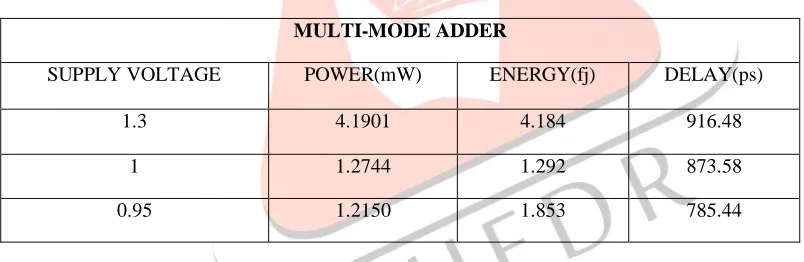
Table 1 Analysis of multimode adder with different supply voltages MULTI-MODE ADDER
SUPPLY VOLTAGE POWER(mW) ENERGY(fj) DELAY(ps)
1.3 4.1901 4.184 916.48
1 1.2744 1.292 873.58
0.95 1.2150 1.853 785.44
The multi-mode adder, using 64-bit carry propagate adder designed for 1.3 v, 1v and 0.95v supply voltages. All the designs ran LTspice and HSPICE tools and results are summarized in Table 1.The energy are very close to the power since the probability of the adder to require more than one cycle is very small.While the energy was cut to 1.85 of the design-ware adder when scaling down to 0.95V,that might be too risky due to process variations sensitivity.
When the supply voltage can be scaled down, the power and energy has been reduced. V. CONCLUSION AND FUTURE WORK
IJEDR1604064 International Journal of Engineering Development and Research (www.ijedr.org) 425 performance of such pipelines. In future, to get better results i.e., low power consumption, energy and reduce delay using CMOS 65 nm technology instead of FINFET 32 nm technology is used.
REFERENCES
[1] Benini L., Macii E., Poncino M. and DeMicheli G. (1998), „Telescopic units: a new paradigm for performance optimization of VLSI designs‟, IEEE Trans. Comput.-Aided Des. Integr. Circuits Syst., vol.17, no.3, pp.220–232.
[2] Chen Y., Li H, Koh C.K., Sun G., Li J., Xie Y. and Roy K. (2010), „Variable latency adder (VL-adder) designs for low power and NBTI tolerance‟, IEEE Trans. Very Large Scale Integr. (VLSI) Syst., vol.18, no.1, pp.1621–1624.
[3] Das S., Dasika G.S., Shivashankar K. and Bull D. (2014), „A 1 GHz hardware loop-accelerator with razor based dynamic adaptation for energy efficient operation‟, IEEE Trans. Circuits Syst.I: Regul. Pap. vol.61, no.8, pp.2290–2298.
[4] Ernst D., Das S., Lee S., Blaauw D., Austin T., Mudge T., Kim N.S and Flautner K. (2004), „Razor: circuit level correction of timing errors for low-power operation‟, IEEE Micro., vol. 6, pp. 10–20.
[5] Freking R.A. and Parhi K.K. (1998), „Theoretical estimation of power consumption in binary adders, in Proceedings of the IEEE International Symposium on Circuits and Systems‟.
[6] Gupta V., Debabrata M., Anand R. and Kaushik R. (2013), „Low-power digital signal processing using approximate adders‟, IEEE Trans. Comput. –Aided Des. Integr. Circuits Syst., vol. 32, no. 1, pp. 124-137. [7] Koren I. (2002), Computer arithmetic algorithms, Universities Press.
[8] Kulkarni P., Gupta P. and Ercegovac M. (2011), „Trading accuracy for power with an under designed multiplier architecture‟, in Proceedings of the 24th
International Conference on VLSI Design, vol.0, pp.346-351.
[9] LaGuiadeSolaz M. and Conway R. (2015), „Razor based programmable truncated multiply and accumulate, energy reduction for efficient digital signal processing‟, IEEE Trans. Very Large Scale Integr. (VLSI) Syst., vol.23, no.1 189–193.