Fabrication, Characterisation and Modelling of Rare-
Earth Doped Alumina (AI2O3) Thin Films for
Optoelectronics
Costas Chryssou
Department o f Electronic and Electrical Engineering
University C ollege London
A thesis submitted to University College, University o f London for the
degree of Doctor o f Philosophy
ProQuest Number: U642226
All rights reserved
INFORMATION TO ALL USERS
The quality of this reproduction is dependent upon the quality of the copy submitted. In the unlikely event that the author did not send a complete manuscript and there are missing pages, these will be noted. Also, if material had to be removed,
a note will indicate the deletion.
uest.
ProQuest U642226
Published by ProQuest LLC(2015). Copyright of the Dissertation is held by the Author. All rights reserved.
This work is protected against unauthorized copying under Title 17, United States Code. Microform Edition © ProQuest LLC.
ProQuest LLC
789 East Eisenhower Parkway P.O. Box 1346
Abstract
The experimental aim of the work presented in this thesis was to determine the suitability of aluminium oxide (AI2O3) as host for rare-earth ions in the production of optically active thin films for optoelectronics.
Two fabrication techniques were used to prepare rare-earth doped AI2O3 thin films; plasma- enhanced chemical vapour deposition (PECVD) and ion implantation. Two A1 PECVD precursors were used; trimethyl-aluminium (TMA) and trimethyl-amine alane (TMAA). A number of AI2O3 thin films were deposited by PECVD on silicon and on silica glass. The thin films were analysed in terms of refractive index, thickness, chemical composition, structure and surface roughness; the optimum deposition conditions were determined. Er^+ -doped AI2O3 thin films were deposited by PECVD using both TMA and TMAA. Er doping of the alumina matrix was achieved using an organic Er precursor; Er(thd)3. Er^+ -doped AI2O3 thin films exhibited broad room-temperature photoluminescence (PL) at 1.533|LLm and 1/e fluorescence lifetime of 2ms. The Er^+ concentration ranged from 0.01At% to 0.2At%. The alumina matrix was co-doped with both erbium and ytterbium by ion implantation. Both AI2O3 PECVD-synthesised thin films and sapphire crystals were used as substrates. Er^+/Yb3+ co-implanted alumina films exhibited very broad room- temperature PL at 1.53|xm. The Er^+ and Yb^+ concentrations ranged from 0.3At% to 0.8At% and from 2.4At% to 8At% respectively. The 1/e fluorescence lifetim e was measured 4.2ms. Both the PL peak intensity and the fluorescence lifetime were studied as a function of the annealing temperature. Evidence for the existence of energy exchange between Er^+ and Yb^+ has been observed.
Acknowledgments
I am indebted to Prof. C. W. Pitt for taking me on in the first place, for his supervision and for finding financial support for the project.
I am particularly grateful to Dr. R. Heinecke and Dr. T. Clapp of Northern Telecom (NORTEL) for sponsoring the project in the first place and for providing access to some of NORTEL facilities at Harlow.
I am also obliged to Dr. A. J. Kenyon for his help with the optical experiments, his helpful discussions and comments through out the research project and for proof-reading the manuscript.
I am particularly grateful to Dr. P. J. Chandler, Mr. D. E. Hole and Prof. P. D. Townsend of the University of Sussex for their invaluable contribution to the ion implantation experiments and their help with the initial lifetime measurements.
A special mention must be given to Dr. F. Di Pasquale for letting me use his theoretical model for analysing rare-earth doped optical waveguides and for all his help with the modelling.
The following people have contributed to the analysis of the thin films:
Dr. J. Milledge of the UCL Geology Department for initial FTIR experiments.
Mr. G. Critchlow of the Institute of Surface Science and Technology, Loughborough University for the AES analysis.
Dr. B. Farmery and Mr. D.E. Hole of the University of Sussex for the RES analysis. Mr. D. Jeffrey for the AFM images.
Mr. N. S. Cohen for the X-ray diffraction analysis.
Mr. K. Lee of UCL for showing me how to use the Talystep and for the SEM analysis. Mr. J. Van Sickle for his help with adapting equipment.
Mr. K. G. Reeves of the UCL Institute of Archeology for the X-ray emission spectroscopy analysis.
Table Of Contents
Page
Abstract
2Acknowledgments
3Table Of Contents
4List Of Tables
8List Of Illustrations
1 0Chapter 1:
Introduction
141 . 1 General Introduction 14
1.2 Outline Of The Thesis 20
References 21
Chapter 2:
Electronic & Optical Properties
Of Rare
-Earth Ions In Solids
252.1 Introduction 25
2.2 Forms Of Aluminium Oxide (AI2O3) 27
2.3 Lattice Sites of Er3+ In AI2O3 29
2.4 Energy Levels Of The Er^+ & Yb^+ Ion 30
2.5 Line Broadening Mechanisms & Radiative Transitions 33 2.6 Multi-Ion Effects In Rare-Earth Doped Materials 34
2.6.1 Like-Ion Interactions 34
2.6.2 Co-Doping 37
2.7 Absorption & Stimulated Emission Cross Sections 39
References 43
Chapter 3:
Process & Analysis Techniques
473.1 Introduction 47
3.2 Plasma-Enhanced Chemical Vapour Deposition (PECVD) 48
3.2.1 Plasmas 48
3.2.2 The PECVD Process And Thin Film Formation 49
3.2.3 The PECVD Apparatus 52
3.4 Thin Film Characterisation Techniques 57
3.4.1 Physical Properties 57
3.4.1.1 Talystep Method 57
3.4.1.2 Ellipsometry 57
3.4.2 Surface Morphology 58
3.4.2.1 Atomic Force Microscopy (AFM) 58
3.4.3 Microstructure - Atomic Positions 59
3.4.3.1 X-Ray Diffraction (XRD) 59
3.4.3.2 Scanning Electron Microscopy (SEM) 59
3.4.4 Chemical Bonding Spectroscopy 60
3.4.4.1 Fourier Transform Infrared (FTIR) Spectroscopy 60
3.4.5 Atom Specific Spectroscopies 60
3.4.5.1 Auger Electron Spectroscopy (AES) 61 3.4.5.2 Rutherford Backscattering Spectrometry (RBS) 61
3.4.5.3 X-Ray Emission Spectroscopy 62
3.4.6 Optical Spectroscopic Methods 62
3.4.6.1 General Characteristics Of The Equipment 62
3.4.6.2 Absorption Measurements 63
3.4.6.3 Photoluminescence Measurements 64 3.4.6.4 Fluorescence Lifetime Measurements 6 6
References 6 8
Chapter 4:
Experimental Results I;
AI
2O
3Thin Films by Plasma-Enhanced
Chemical Vapour Deposition (PECVD)
704.1 Introduction 70
4.2 Aluminium Precursors 71
4.2.1 Trimethyl-aluminium (TMA) 71
4.2.2 Trimethyl-amine alane (TMAA) 72
4.3 Deposition Of AI2O3 Thin Films By PECVD 74
4.3.1 Using Trimethyl-aluminium (TMA) 74
4.3.2 Using Trimethyl-amine alane (TMAA) 80
4.3.3 FTIR Spectroscopy Analysis 93
4.4 Summary 95
Chapter 5:
Experimental Results II;
Er^+ -Doped AI
2O
3Thin Films by
Plasma-Enhanced Chemical Vapour
Deposition (PECVD)
5 . 1 Introduction
5.2 Rare-Earth Precursors
5.3 Er2 0 3 Thin Films By PECVD
5.4 Er3+ -Doped AI2O3 Thin Films By PECVD 5.4.1 Photoluminescence Spectra 5.4.2 Thermal Annealing
5.4.3 Defect Luminescence 5.4.4 Fluorescence Lifetime 5.5 Summary
References
Chapter
6:
Experimental Results HI;
Er^+ And Yb^+ Co-Implanted AI
2O
3Thin Films And Sapphire Crystals
6 . 1 Introduction
6.2 Ion Ranges And Implant Concentration Profiles 6.3 Photoluminescence Spectra
6.4 Energy Exchange Between Yb^+ And Er^+ 6.5 Defect Luminescence
6.6 Thermal Annealing 6.7 Fluorescence Lifetime 6.8 Summary
References
Chapter 7:
Computer Modelling;
Signal Gain Characteristics Of Er^+
-Doped AI
2O
3Channel Optical
Waveguides
7 . 1 Introduction 7.2 Theoretical Model
7.5 Possible Applications 160
7.6 Summary 165
References 167
Chapter 8:
Conclusions
1698.1 Summary Of Objectives 169
8.2 Summary Of Achievements 169
8.3 Future Work 171
References 173
Appendix A :
List Of Publications
174List Of Tables
Chapter 2
Table 2.1 : The rare-earth elements (lanthanides).
Table 2.2: Characteristics of polymorphic forms of AI2O3.
Table 2.3: Peak emission cross sections of Er^+ in various host materials.
Chapter 3
Table 3.1: Typical operating parameters for the deposition of AI2O3 thin films.
Chapter 4
Table 4.1: The basic characteristics of TMA. Table 4.2: The basic characteristics of TMAA.
Table 4.3: The deposited AI2O3 thin films using TMA. Table 4.4: The deposited AI2O3 thin films using TMAA. Table 4.5: Reflection peaks of various forms of AI2O3.
Table 4.6: Infrared band assignment for plasma deposited AlOx films.
Chapter 5
Table 5.1: The structures of (3-diketones used as ligands.
Table 5.2: Deposition conditions of Er2 0 3 thin films deposited by PECVD using Er(thd) 3 as the Er precursor.
Table 5.3: The deposition conditions of Er^+ -doped AI2O3 thin films using TM A and TMAA as the A1 precursor.
Table 5.4: 1500nm bandwidths for Er^+ -doped materials.
Chapter 6
Table 6.1: The PECVD-deposited AI2O3 thin films and the sapphire crystals implanted with both Yb and Er.
Table 6.2: Peak Yb^+ and Er^+ concentrations corresponding to the three Yb3+/Er3+ concentration ratios.
Table 6.7: The linear thermal expansion coefficient (a) for Si, quartz Si0 2 and AI2O3. Table 6 .8: PL peak intensity and FW HM of the emission spectra from as-implanted Er3+/Yb^+ co-implanted AI2O3 thin films deposited on quartz Si0 2 glass.
Table 6.9: PL peak intensity and FW HM of the emission spectra from as-implanted Er^+/Yb^+ co-implanted sapphire crystals.
Table 6.10: Defect luminescence intensity from two Er3+/Yb^+ co-implanted AI2O3 thin films.
Table 6.11: Fluorescence lifetime of some Er^+/Yb^+ co-implanted AI2O3 thin films and sapphire crystals, as-implanted and following thermal annealing in air at 950°C for 90min.
Chapter 7
Table 7.1: Input parameters to the model used for the theoretical analysis of Er^+ -doped Si0 2 waveguides.
List of Dlustrations
Chapter 1
Figure 1.1: (a) A schematic of an EDFA and (b) the three level lasing system provided by
Er3+.
Figure 1.2: Schematic of an Er^+ -doped planar amplifier.
Chapter 2
Figure 2.1: Schematic of the crystal structure of a-A l2 0 3 (sapphire). Figure 2.2: The y-Al2 0 3 structure (defect spinel structure).
Figure 2.3: Energy levels of Er^+. Figure 2.4: Energy levels of Yb3+.
Figure 2.5: Absorption of Er^+ -doped silicate glass.
Figure 2.6: Schematic of three different concentration quenching effects in Er3+.
Figure 2.7: Schematic energy level diagram showing the energy transfer between donor and acceptor in a system doped with two different rare-earth ions.
Figure 2.8: Absorption spectrum of an Yb3+/Er3+ Si0 2 optical fibre.
Chapter 3
Figure 3.1: The thin film formation.
Figure 3.2: The PECVD reaction chamber and the gas delivery system. Figure 3.3: A schematic of the 200keV implantation system.
Figure 3.4: Block diagram of the experimental set-up used to measure the absorption spectrum.
Figure 3.5: Block diagram of the experimental set-up used to measure the PL spectrum. Figure 3.6: The second experimental set-up used to measure the fluorescence lifetime.
Chapter 4
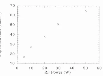
Figure 4.1 : Deposition rate as a function of the substrate temperature. Figure 4.2: Deposition rate as a function of the RF power.
Figure 4.3: Refractive index as a function of the RF power. Figure 4.4: AES depth profile of the AI2O3 sample AS2.
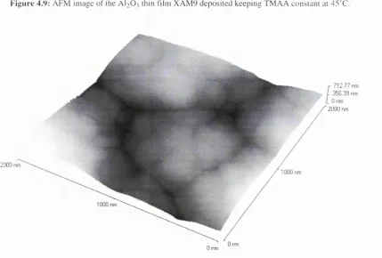
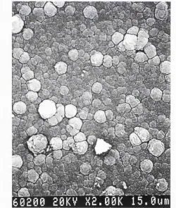
Figure 4.9: AFM image of the AI2O3 thin film XAM9. Figure 4.10: AFM image of the AI2O3 thin film XAM7. Figure 4.11: SEM picture of the AI2O3 thin film XAM7.
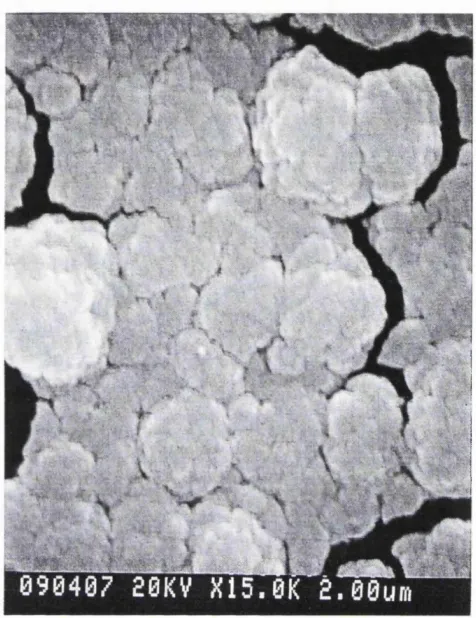
Figure 4.12: SEM picture of a part of the same area as Figure 4.11 but at greater magnification.
Figure 4.13: Deposition rate of the AI2O3 thin film deposited using TMAA as a function of the RF power.
Figure 4.14: X-ray diffractograms of the AI2O3 sample XAMIO: (a) as grown and (b) following annealing at 600°C for 2h.
Figure 4.15: X-ray diffractograms of the AI2O3 sample XAMIO: (a) following annealing at 1000°C for 2h and (b) following annealing at 1200°C for 5h.
Figure 4.16: AES depth profile of the AI2O3 sample XAM3.
Figure 4.17: AES depth profiles of the AI2O3 samples XAM4 and XAM6. Figure 4.18: AES depth profiles of the AI2O3 sample XAM7 and XAMIO.
Figure 4.19: FTIR spectra of the AI2O3 sample AS4 as-grown and following thermal annealing at 600°C for 90min.
Figure 4.20: FTIR spectra of the AI2O3 sample XAM7 as-grown and following thermal annealing at 600°C for 90min.
Chapter 5
Figure 5.1: The TGA curve for Er(thd) 3 compound.
Figure 5.2: Deposition rate of Er2 0 3 thin films as a function of the Er(thd) 3 temperature. Figure 5.3: X-ray emission spectroscopy analysis of the Er2 0 3 thin film ER5.
Figure 5.4: AES depth profiles of the Er^+ -doped AI2O3 thin films XAM23 and XBL4. Figure 5.5: AES depth profile of the Er^+ -doped AI2O3 thin film XML2.
Figure 5.6: Room-temperature photoluminescence spectrum of the Er^+ -doped AI2O3 thin film XML2 deposited by PECVD using TMA.
Figure 5.7: Room-temperature photoluminescence spectrum of the Er^+ -doped AI2O3 thin film X B L31 deposited by PECVD using TMAA.
Figure 5.8: Photoluminescence spectrum of the sample XML2 at 65K. Figure 5.9: Photoluminescence spectrum of the sample XBL31 at 65K. Figure 5.10: PL peak intensity as a function of the sample temperature.
Figure 5.11: FTIR spectra of the Er^+ -doped AI2O3 sample XML2 as grown and following thermal annealing in air at 950°C for 90min.
Figure 5.15: Fluorescence decay of the sample XML2 together with the best single exponential fit.
Figure 5.16: Fluorescence decay of the sample XML2 together with the best double exponential fit.
Chapter 6
Figure 6.1 : Concentration profiles for batch #1, (a) for Yb and (b) for Er. Figure 6.2: Concentration profiles for batch #2, (a) for Yb and (b) for Er. Figure 6.3: Concentration profiles for batch #3, (a) for Yb and (b) for Er.
Figure 6.4: Room-temperature PL spectrum from the as-implanted Er3+/Yb^+ co-implanted AI2O3 thin film YAM6 pumped at 514nm.
Figure 6.5: Room-temperature PL spectrum from the as-implanted Er^+/Yb3+ co-implanted sapphire crystal SI pumped at 514nm.
Figure 6.6: Room-temperature PL spectrum from the as-implanted Er^+ZYb^^ co-implanted AI2O3 thin film YAM 13 pumped at SOOnm.
Figure 6.7: Room-temperature PL spectrum from the as-implanted AI2O3 thin film YAM 13 pumped at 840nm. Absorption is primarily due to Yb^+.
Figure 6.8: PL peak intensity as a function of the Yb^+/Er3+ concentration ratio.
Figure 6.9: Normalised PL peak intensity as a function of the pump wavelength for the sample YAM 12.
Figure 6.10: Defect luminescence spectra from the sample Im l as-implanted and following thermal annealing at 950°C for 90min.
Figure 6.11: Defect luminescence spectrum from the as-implanted sample S 1.
Figure 6.12: Defect luminescence spectra from the PECVD-grown AI2O3 sample AS2 as- grown and following ion implantation.
Figure 6.13: PL peak intensity as a function of the annealing temperature.
Figure 6.14: Room-temperature PL spectra from the AI2O3 sample Im l as-implanted and following thermal annealing at 850°C, 900°C and 950°C for 90min.
Figure 6.15: Fluorescence decay of the sample Im l with the best single exponential fit. Figure 6.16: Fluorescence lifetime as a function of the annealing temperature.
Figure 6.17: Fluorescence decay of the as-implanted sample Im8 with the best single exponential fit.
Chapter 7
Figure 7.5: Signal gain as a function of the input pump power. Figure 7.6: Simulated transmission system
Figure 7.7: ASE filter used in the computer simulation.
Chapter ] : Introduction
Chapter 1 : Introduction
1.1 General Introduction
Photonics technology today is a driving force for many technological developments. Because of its enormous speed and bandwidth, photonics can speed up computers dramatically and will yield a wealth of sophisticated telecommunication services. Future information superhighways will also be based on photonic technology [1].
R are-earth ions, in particular erbium (Er), have played an im portant role in the development of optical communication technology and systems in the last decade. Er^+ (the preferred bonding state) has an incomplete 4f electronic shell that is partially shielded from perturbation by external fields by closed 5s and 5p shells [2-5]. Transitions are not normally allowed, but in a solid host, mixing of states changes symmetry. As a result, sharp optical intra-4f transitions can be achieved from Er3+ -doped materials. Er^+ is particularly attractive because its emission wavelengths, around 1.53|Lim, coincide with the low attenuation region of silica (Si0 2 ) optical fibres.
In 1987 it was discovered [6, 7] that Er^+ -doped Si0 2 optical fibres could be used as optieal amplifiers operating at 1.54]Lim. A sehematic diagram of an Er^+ -doped fibre amplifier (EDFA) is shown in Figure 1.1(a); Figure 1.1(b) shows the three level lasing system provided by Er^+. The principle is well known; when a signal photon (wavelength around 1.54|im) encounters Er^+ ions within an optical fibre that are excited to higher energy levels by a continuous pump laser source, the signal power gradually increases along the optical fibre by stimulated emission [3, 4, 6-10].
C h a p te r 1 : Introduction
Signal
input Coupler
Diode
pump Er^+ -doped fibre
A m plified signal output
High energy level
Pump
photon Signalphoton
M etastahle level T~10ms
Signal photon
Stim ulated photon
b
F ig u re 1.1: (a) A schematic o f an E D F A and (b) the three level lasing syste m provided by Er^+ [10].
P r a c t i c a l p u m p w a v e l e n g t h s fo r E r - d o p e d m a t e r i a l s are 0 . 9 8 p m , at w h i c h i n e x p e n s i v e
la s e rs a re a v a i l a b l e , a n d 1 .4 8 p m . It is r e p o r te d th at g a in p u m p e f f i c i e n c y at 0 . 9 8 p m m a y
be i m p r o v e d to 4 . 9 d B / m W , th re e tim e s h ig h e r th a n th a t o f 1 .4 8 p m p u m p - w a v e l e n g t h [8,
1 1]. T o d a te o n e o f th e m o s t im p r e s s i v e t r a n s m i s s i o n e x p e r i m e n t s r e p o r ts a t r a n s m i s s i o n
o v e r IbOOOKm o f f i b r e at 2 .4 G b i t s / s w ith less th a n 10^ b i t - e r r o r r a te u s i n g a d i r e c t -
m o d u l a t i o n la s e r t r a n s m i t t e r [12]. R e c e n t l y , a m u l t i w a v e l e n g t h o p tic a l t r a n s m i s s i o n rate
as h ig h as lO OGbits/s w a s d e m o n s t r a t e d in a 6 3 0 0 K m l o n g f i b r e link w ith fib re a m p l i f i e r s
C h ap ter 1 : Introduction
B e c a u s e o f t h e ir e y lin d r ic a l g e o m e t r y a n d t h e ir larg e le n g th ( s e v e r a l m e te r s ) E D F A 's are
n o t s u i t a b l e as e o m p o n e n t s fo r in te g r a te d p l a n a r o p tic a l c irc u its . T h e c h a l l e n g e , h o w e v e r ,
lie s in o p t o e l e c t r o n i c i n t e g r a t i o n , in w h i c h e l e c t r i c a l a n d p h o t o n i c t e c h n o l o g i e s are
s y n t h e s i s e d in o n e s y s t e m , a l l o w i n g i n f o r m a t i o n to be g e n e r a t e d , t r a n s p o r t e d , s w i t c h e d ,
a n d r e c e i v e d as lig h t [1]. A lo g ical s te p in o p tic a l a m p l i f i e r d e v e l o p m e n t is th e p l a n a r
a m p l i f i e r , in w h i c h Er^+ - d o p e d c h a n n e l w a v e g u i d e s a re m a d e on a p l a n a r s u b s t r a t e .
T h e r e f o r e , in th e last fe w y e a rs , ra re -e a rth d o p e d p l a n a r o p tic a l w a v e g u i d e s h a v e r e c e iv e d
a lot o f a t t e n t i o n b e c a u s e o f th e ir p o t e n tia l a p p l i e a t i o n in in t e g r a t e d o p tic s . R a rc -e a i ih
d o p i n g o f c h a n n e l w a v e g u i d e s f a b r i c a t e d in a r a n g e o f m a t e r i a l s o ffe rs the p o s s ib ilitv o f
c o n s t r u c t i n g a c t i v e d e v i c e s th a t c a n p l a y i m p o r t a n t r o l e s in o p t i e a l c o m m u n i c a t i o n
s y s t e m s [4]. T h i s te c h n o l o g y e n a b le s the c o n s t r u c t i o n o f o p tic a l a m p lif ie r s , la s e rs o r m o re
c o m p l i c a t e d d e v i c e s / s y s t e m s o n s u b s tr a te s w ith m u c h s h o r t e r w a v e g u i d e s th a n th e fib re-
b a s e d s y s t e m s . P l a n a r w a v e g u i d e a m p l i f i e r s o f f e r the i m p o r t a n t a d v a n t a g e th at th e y c an
be in t e g r a t e d w ith o t h e r w a v e g u i d e d e v ic e s s u c h as s p litte rs , s w i t c h e s , o r m u l t i p l e x e r s on
a s i n g l e c h ip . A s c h e m a t i c o f an Er^+ - d o p e d w a v e g u i d e a m p l i f i e r ( E D W A ) is s h o w n in
F i g u r e 1.2. A l t h o u g h E D W A ' s s h o w c o n s i d e r a b l y le ss o p t i c a l g a i n t h a n E D F A ' s ,
E D W A ' s h a v e th e a d v a n t a g e o v e r th e i r f i b r e e o u n t e r p a r t s o f e a s e o f m a s s p r o d u c t i o n ,
m i n i a t u r i s a t i o n , c o m p a c t n e s s , co st an d p a c k a g i n g [14].
Signol
P um p
Signa!
F igu re 1.2: S chem atic o f an EF+ -doped planar am plifier (A M P ) integra ted with a 1x4 splitter (S PL ) on a
Chapter 1: Introduction
The radiative lifetime of the first excited state of Er^+ is in the m illisecond range, depending on the material. As a result, the emission and absorption cross sections are relatively small (typically 10'^^ - lO'^Ocm^). Therefore, to achieve reasonable signal gain (~3dB), it is important that the signal beam encounters a large number of excited Er^+ ions. Given the small length of Er^+ -doped planar waveguides, concentrations ranging between 0.1 At% and lA t% are necessary. However, at such high Er^+ concentrations the Er^+ ions are not uniformly distributed anymore in the host material but they tend to interact with each other and form clusters; clustering of the Er^+ ions reduces the gain perform ance of the optical amplifier. The biggest barrier to obtaining efficient planar waveguide amplifiers with high gain is both uniform and ion-pair (clustered) induced up- conversion. The up-conversion mechanism takes place between two excited (in the level) Er3+ ions which interact with each other promoting one ion into the 4lg/ 2 Er^+ state leaving the other one in the ground state. Thus, the degree of population inversion at a given pump power is reduced. Another problem is the difficulty of fabricating a well- confined low-loss waveguide using material suitable for amplifier. However, such waveguides can be obtained by optimising the fabrication processes. Thus, the focus is on degradation resulting from up-conversion. This up-conversion process depends strongly on both the host material and the Er^+ concentration.
W hen this research started, in 1994, Er^+ -doped Si0 2 planar waveguides had been thoroughly investigated and successfully fabricated by several groups using various fabrication techniques; this is mainly because of their compatibility with existing Si0 2 optical fibre technology. Two main approaches were followed for the fabrication of optical am plifiers with high signal gains; the first one was using very high Er^+ concentrations (1 x 10^^ - 6 x 10^0 ions/cm^) [15, 16] and short optical waveguides (2cm - 4cm) and the other using relatively small Er^+ concentrations (~4 x 10'^ ions/cm^) and long optical waveguides (20cm - 36cm) [17, 18].
Chapter 1: Introduction
1.53)im signal wavelength. The high Er^+ concentrations used, however, reduce the lifetime of the metastable level; in addition, the achievable signal gain is quenched due to up-conversion. Therefore, a recent publication by the same group reports the use of a much lower (7 x lO^^ions/cm^) Er^+ concentration; as a result a very low threshold pump power (8mW) at 0.98p.m was achieved with a net optical gain of 4.5dB at 80mW of pump power at a signal wavelength of 1.536p.m.
A nother research group reports the first attempt to integrate a 980/1530nm wavelength division m ultiplexing (WDM) coupler with an Er^+ -doped silica-based waveguide amplifier [17]. A high gain of 27dB and a low noise figure of 5dB were realised with the waveguide amplifier integrated with the WDM coupler. The Er^+ -doped waveguide had an Er^+ concentration of -3.7x10^^ ions/cm^ and a total length of 47.7cm. This high signal gain was measured for pump power of 264mW at 0.98|utm and a signal wavelength of 1.533p.m.
Apart from being used for signal amplification at 1.54pm, EDWA's can also be used for loss compensation towards transparent optical networks [19, 20]. The realisation of a 23cm long optical beam splitter consisting of Er^+ -doped optical waveguides has already been reported [19]. It compensates for the total device loss, including the principal splitting (3dB) and the propagation losses when pumped with 60mW at 0.98pm . Moreover, it exhibited 8dB net signal gain when pumped with 170mW.
In addition to Er^+ -doped materials, there are many reports on co-doping the erbium system with another rare-earth ion, in particular with ytterbium (Yb) [10, 21-25]. The co doping technique is an attractive mean of alleviating constraints on the pump source wavelength by using a sensitiser with a broad absorption band. Ytterbium is especially attractive in this regard as it exhibits an intense broad absorption between 800nm- 1080nm. A small Er3+/Yb^+ ion-ion separation provides a very efficient indirect pumping m echanism for Er^+ and may also allow doping with extrem ely high erbium concentrations without serious gain and pump efficiency reduction due to up-conversion
Chapter 1: Introduction
They should also be uniform and free from scattering and absorption losses [27]. As a rough figure attenuations of IdB/cm or less are desirable. For most applications the absolute value of the refractive index is of secondary importance. Although there is in principle no disadvantage in applying high refractive index materials, low refractive index materials have some advantages. A low index facilitates coupling to optical fibres. Furthermore, with low indices (n<1.8) light can be coupled into the film with high index glass prisms [28].
A lum inium oxide (AI2O3) thin films are of interest for various applications such as m icroelectronics, coatings, catalysis and advanced material technology [29, 30]. The properties m ost im portant for m icroelectronics are high dielectric constant, low permeability of alkali ions and high thermal conductivity [30, 31]. Moreover, alumina's hardness (Mohs 9), its stability at high temperatures and its inertness against a wide range of chemicals make it extremely attractive for protective coatings.
AI2O3 is an interesting material as host for rare-earth ions because the feasibility of producing high quality AI2O3 waveguides has been demonstrated. Thus, AI2O3 thin film optical waveguides have been recently fabricated with attenuation as low as 0.38 dB/cm [32]. Moreover, its refractive index is low enough to apply glass prisms and a contacting liquid and high enough to provide good optical contrast with Si0 2 or glass to be used as cladding layers. Furtherm ore, it is a stable oxide. Si0 2 /Al2 0 3/Si0 2 structures are attractive because they can be formed on oxidised Si substrates [28].
W hile this research work was heading towards its completion, AI2O3 received a lot of attention as host for Er^+. An impressive signal gain of 2.3dB was achieved at 1.53p.m from a 4cm long Er^+ -implanted AI2O3 optical waveguide when pumped with only 9mW of pump power at 1.48p.m. This improved performance of the AI2O3 waveguides can be attributed to the better solubility of Er^+ in AI2O3 matrix compared to Si0 2 [32].
Chapter 1; Introduction
This research work demonstrated that optically active Er^+ -doped AI2O3 thin films can be deposited by PECVD using an organic precursor as the Er source material. In addition, this thesis reports the incorporation of both Er and Yb in the AI2O3 matrix by ion implantation, and the demonstration of very broad Er^+ photoluminescence.
1.2 Outline Of The Thesis
Following the introduction, where a general overview of the research on Er^+ -doped and Er^+/Yb^+ co-doped planar optical waveguide amplifiers is given, chapter 2 describes the electronic and optical properties of the rare-earth ions when incorporated in solids. Chapter 2 gives also an account of the dissipative processes that manifest themselves due to the high Er^+ concentrations needed to achieve reasonable signal gains in EDWA's. Chapter 3 gives a detailed description of the PECVD and ion implantation processes used for the preparation of the thin films and presents all the analysis techniques used for the characterisation of the AI2O3 and rare-earth doped AI2O3 thin films. The choice of precursors and the experimental results are presented in chapters 4, 5 and 6.
Chapters 4, 5 and 6 describe the experimental results achieved from the AI2O3, Er^+ -doped AI2O3 and Er3+/Yb3+ co-im planted AI2O3 thin film s, respectively. A fter presenting the structural and chemical characterisation of the AI2O3 thin films, the fluorescence spectra and lifetime measurements are displayed for both the Er3+ -doped and Er^+ /Yb3+ co-implanted AI2O3 thin films. The results confirm that fluorescent rare- earth doped AI2O3 thin films can be produced by both PECVD and ion implantation. Some evidence of the existence of an energy transfer mechanism between Er^+ and Yb^+ is also presented.
Chapter 7 predicts the signal gain from Er^+ -doped AI2O3 thin films by PECVD. The model is based on the experimental results acquired from the PECVD grown erbium- doped alumina thin films. It is shown that Er^+ -doped AI2O3 optical waveguides show improved gain characteristics compared to Er^+ -doped Si0 2 optical waveguides. In addition, the performance of WDM transmission systems consisting of Er3+ -doped AI2O3 and Er^+ -doped Si0 2 waveguide amplifier cascades are analysed and compared.
Chapter 1 : Introduction
References
[1] A. Polman, "Erbium Ion Implantation For Optical Doping," Mat. Res. Symp.
Proc., Vol. 316, pp. 385-396, 1994.
[2] A. Polman, "Erbium implanted thin film photonic materials," J. Appl. Phys., Vol.
82, pp. 1-39, 1997.
[3] P. Urquhart, "Review of rare earth doped fibre lasers and amplifiers," lE E Proc.,
Vol. 135, pp. 385-407, 1988.
[4] P.W. France (ed.): Optical Fibre Lasers and Amplifiers (Blackie, London, 1991).
[5] M.J.F. Digonnet (ed.): Rare earth doped fiber lasers and amplifiers (Marcel
Dekker, 1993).
[6] E. Desurvire, R.J. Simpson, P.C. Becker, "High Gain Erbium-Doped Traveling-
Wave Fiber Amplifier," Opt. Lett., Vol. 12, pp. 888-890, 1987.
[7] R.J. Mears, L. Reekie, I.M. Jauncey, D.N. Payne, "Low Noise Erbium-Doped
Fiber Amplifier Operating at 1.54pm," Electron. Lett., Vol. 23, pp. 1026-1028, 1987.
[8] K. Nakagawa, S. Shimada, "Optical Amplifiers in Future Optical
Communication Systems," IEEE ECS Magazine, Vol. 1, pp. 57-62, 1990.
[9] J. Senior: Optical Fiber Communications; Principles and Practice (2nd edition,
Prentice Hall, 1992).
[10] D. Payne, "Active Fibres and Optical Amplifiers," Fiber and Integrated Optics,
Vol. 11, pp. 191-219, 1992.
[11] M. Shimizu," Compact and highly efficient optical fibre amplifier module
pumped by a 0.98pm laser diode," OFC'90, PD-17, 1990.
[12] N.S. Bergano, J. Aspello, C.R. Davidson, P.R. Trischitta, B.M. Nyman, F.W.
Kerfoot, "Bit Error Rate Measurements Of 14000km 5 Gbit/S Fiber-Amplifier
Chapter 1: Introduction
[13] N.S. Bergano, C.R. Davidson, F. Heismann, "Bit Synchronous Polarization and
Phase Modulation Scheme for Improving the Performance of Optical Amplifier Transmission," Electron. Lett., Vol. 32, pp. 52-54, 1996.
[14] H. Takahashi, K. Okamoto and Y. Ohmori, "Integrated-optic 1 x 128 power splitter with multifunnel waveguide," IEEE Photonics Techn. Lett., Vol. 5, pp. 58- 60, 1993.
[15] J. Shmulovich, A. Wong, Y.H. Wong, P.C. Becker, A.J. Bruce, and R. Adar,
"Er3+ Glass Waveguide Amplifier At 1.5|Lim On Silicon," Electron. Lett., Vol. 28, pp. 1181-1182, 1992.
[16] G. Nykolak, M. Haner, P.C. Becker, J. Shmulovich, Y.H. Wong, "Systems
Evaluation of an Er^+ -Doped Planar Waveguide Amplifier," IEEE Photonics Techn. Vol. 5, pp. 1185-1187, 1993.
[17] K. Hattori, T. Kitagawa, M. Oguma, Y. Ohmori, M. Horiguchi, "Erbium- Doped Silica-Based Waveguide Amplifier Integrated With A 980/1530nm WDM Coupler," Electron. L ett, Vol. 30, pp. 856-857, 1994.
[18] T. Kitagawa, K. Hattori, K. Shuto, M. Oguma, J. Temmyo, S. Suzuki, M.
Horiguchi, "Erbium-Doped Silica-Based Planar Amplifier Module Pumped by
Laser Diodes," I9th European Conference on Optical Communication, Montreux, Paper THC 12.11, 1993.
[19] T. Kitagawa, "Rare-Earth-doped Planar Waveguide Amplifiers," Optical
Amplifiers A nd Their Applications Technical digest, Yokohama, Paper M C I, pp. 136-139, 1993.
[20] C.E. Chryssou, M.F. Federighi, C.W. Pitt, "Lossless Stripe Waveguide Optical Beam Splitter: Modeling of the Y-Structure," lEEE/OSA J. Lightwave Techn.,
Vol. 14, pp. 1699-1703, 1996.
[2 1] P. Laporta, S. De Silvestri, V. Magni, O. Svelto, "Diode-pumped cw bulk Er:Yb
glass laser," Optics Lett., No\. 16, pp. 1952-1954, 1991.
Chapter 1: Introduction
[23] J.M.P. Delavaux, S. Granlund, O. Mizuhara, L.D. Tzeng, D. Barbier, M.
Rattay, F. SaintAndre, A. Kevorkian, "Integrated optics erbium-ytterbium
amplifier system in 10-Gb/s fiber transmission experiment," IEEE Photonics Techn. Lett., Vol. 9, pp. 247-249, 1997.
[24] D. Barbier, M. Rattay, F. SaintAndre, G. Clauss, M. Trouillon, A.
Kevorkian, J.M.P. Delavaux, E. Murphy, "Amplifying four-wavelength
combiner, based on erbium/ytterbium-doped waveguide amplifiers and integrated splitters, " IEEE Photonics Techn. Lett., Vol. 9, pp. 315-317, 1997.
[25] P. Fournier, P. Meshkinfam, M.A. Fardad, M.P. Andrews, S.I. Najafi,
"Potassium ion-exchanged Er-Yb doped phosphate glass amplifier," Electron. Lett., Vol. 33, pp. 293-295, 1997.
[26] F.Di Pasquale, M. Federighi, "Improved gain characteristics in high- concentration Yb^+ / Er^+ co-doped glass waveguides amplifiers", IEEE J. Quantum Electron., Vol. 30, pp. 2127-2131, 1994.
[27] A.H. Bailey, D.A. Darbyshire, A.P. Overbury, C.W. Pitt, J. Newton, "Plasma deposition of metal oxide films for integrated optics," Vacuum, Vol. 36, pp. 139-
142, 1986.
[28] M.K. Smit, G.A. Acket, C.J. van der Laan, "AI2O3 Films For Integrated Optics," Thin Solid Films, Vo\. 138, pp. 171-181, 1986.
[29] B. Ealet, M.H. Elyakhloufi, E. Gillet, M. Ricci, "Electronic and crystallographic structure of y-alumina thin films," Thin Solid Films, Vol. 250, pp. 92-100, 1994. [30] Y. Wen Zhao, H. Suhr, "Aluminium Oxide Thin Films Prepared by Plasma-
Enhanced Chemical Vapour Deposition," Appl. Phys. A, Vol. 55, pp. 176-179, 1992.
[31] J.S. Kim, H.A. Marzuk, P.J. Reucroft, J.D. Robertson, C.E. Hamrin,
Chapter 1: Introduction
[32] G.N. van den Hoven, R.J.I.M. Koper, A. Polman, C. van Dam, J.W.M. van
Uffelen, M.K. Smit, "Net optical gain at 1.53|Lim in Er-doped AI2O3 waveguides
Chapter 2; Electronic & Optical Properties Of Rare-Earth Ions In Solids
Chapter 2 : Electronic & Optical Properties Of
Rare-Earth Ions In Solids
2.1 Introduction
This chapter presents the basic physical ideas behind the incorporation of the rare-earth elements into solids. Apart from presenting the lanthanides and the Er and Yb energy levels this chapter discusses the influence of the host material on the rare-earth ions and also presents the ion-ion interaction effects that arise due to the high doping levels needed for producing efficient rare-earth doped planar optical amplifiers.
Rare-earth ions have important characteristics that distinguish them from other optically active ions: they emit and absorb over narrow wavelength ranges, the wavelengths of the emission and absorption transitions are relatively insensitive to host material, the intensities of these transitions are weak and the lifetimes of metastable levels are long [1].
The rare-earth elem ents are divided into two groups of fifteen elem ents each. The lanthanides are characterised by the filling of the 4f shell and begin with lanthanum (La, Z=57) and end with lutetium (Lu, Z=71) [1-4]. The actinides fill the 5f shell from thorium (Th, Z=71) to lawrencium (Lw, Z=103). Although actinides show the same electronic properties with the lanthanides only the latter are of great importance to lasers and amplifiers since many actinides have no isotopes stable enough to be useful for such devices [1]. Table 2.1 shows the lanthanides together with their atomic num ber and electron configuration both as neutral atoms and in the +3 ionisation state. As it can be seen all the rare-earth atoms have the same outer electronic structure 5s^5p^6s^, which are filled shells. The num ber of electrons occupying the inner 4f shell dictates their optical characteristics [2, 3]. La has zero and Lu has fourteen 4f electrons. Optical absorption and emission causes transitions within the 4f shell. Ionisation of the rare-earths usually takes place to form a trivalent state to give, for example Er^+. During ionisation, two of the 6s electrons and one of the 4f electrons are removed, but the outer 5s and 5p shells remain intact [2, 3].
Chapter 2: Electronic & Optical Properties Of Rare-Earth Ions In Solids
by the hope of using semiconductors to achieve electrical pumping of rare-earth centres instead of the optical excitation. Moreover, Er^+ -doped Si is very attractive because if efficient light emission could be achieved from this material, the integration of electrical and optical functions on a single chip may be realised. Rare-earth doped waveguides in LiNbOg have also been reported; these waveguides could be used to produce splitters and modulators which can compensate for their intrinsic losses [5, 11].
T a b le 2 .1 ; T h e rare-earth e le m e n ts (la n th a n id e s ) s h o w in g the a to m ic num ber and th e e le c tr o n co n fig u ra tio n for both as neutral atom s and in the +3 ion isation state. (X e ) corresp on d s to the electron co n fig u ra tio n o f a neutral X en o n atom , i.e. ls^2s^2p^3s^3p^3d^®4s^4p^4d'®5s^5p^ [2, 3].
Rare-earth elem en ts
A tom ic num ber
E lectron configuration (neutral atoms)
E lectron co n fig u ra tio n
(io n s )
Lanthanum (La) 57 (X e) 6s25d (X e)
C erium (C e) 58 (Xe)6s^4f5d (X e)4P
Praceodym ium (Pr) 59 (X e)6s24f3 (X e)4f2
N eodym ium (Nd) 60 (X e)6s24f4 (Xe)4f^
P rom ethium (Pm ) 61 (Xe)6s^4f5 ( X e ) 4 f
Sam arium (Sm ) 62 (Xe)6s^4f6 (Xe)4f^
E uropium (Eu) 63 (X e )6 s 2 4 f (Xe)4I^
G adolinium (Gd) 64 (X e)6s24E 5d (X e)4 T
Terbium (Tb) 65 (X e)6s24f9 (Xe)41^
D ysprosium (D y) 66 (X e)6s24f'0 (X e)4f9
H olm iu m (H o) 67 (X e)6s^ 4f" (X e)4 f'o
Erbium (Er) 68 (X e)6s24fi2 (X e )4 f'i
T hulium (Tm ) 69 (X e)6 s2 4 p 3 (X e)4f'2
Y tterbium (Y b) 7 0 (Xe)6s24f>4 (X e)4fi3
L utetium (Lu) 71 (Xe)6s24f>^5d (X e)4 p 4
Chapter 2: Electronic & Optical Properties Of Rare-Earth Ions In Solids
been explained in [14] : Erbium oxide (8 :2 0 3) dissolves more in AI2O3 than in Si0 2 . Thus, when Si0 2 is co-doped with Al, AI2O3 forms a solvation shell around the rare-earth ion and the resultant complex is readily incorporated into the Si0 2 network reducing the amount of clustering [14].
As it was discussed in chapter 1, in order to achieve reasonable signal gain from Er3+ -doped optical waveguides, high Er^+ concentrations have to be incorporated in the host material (~lA t% ). Rare-earth ions require large co-ordination numbers, i.e. the number of nearest neighbour atoms must be high; the absence of a sufficient number of non-bridging oxygens to co-ordinate isolated rare-earths causes them to cluster in order to share non bridging oxygens [4]. AI2O3 introduces a larger number of non-bridging oxygens than Si0 2 and therefore increases the co-ordination number of the Er^+ ions. For example, it is reported that the Er^+ ion is situated in an eight-fold and twelve-fold co-ordinate site in crystals of Y3AI5O1 2 and YAIO3 respectively whereas in silicate glasses the Er^+ ion is six fold co-ordinated [15]. The larger co-ordination number of the Er3+ ions in AI2O3 and the need to find a host where high Er^+ concentrations could be incorporated without dramatic concentration quenching effects led research to AI2O3 host.
2.2 Forms Of Aluminium Oxide (AI
2O
3)
Stoichiometrically there is only one oxide of aluminium; alumina (AI2O3). However, this simplicity is compensated by the fact that alumina exists in various polymorphs, hydrated species and so on, the formation of whieh depends on the conditions of preparation [16- 23]. There are accounts of the formation of 5 or even 6 modifications of alumina: a , (3, y, y , a , £ [16-23]. The characteristics of the main types of AI2O3 are given in Table 2.2 [16].
Table 2 .2 : C haracteristics o f p olym orp h ic form s o f A I2O3 [1 6 , 17].
Form S y ste m H abit S p e c ific
G ravity
R efra ctiv e In d ex
R eaction to heating
a -a lu m in a
(corundum)
H exagonal Tablets and
rhombohedra
3.99 1.768 Melts at
2050°C
(3-alumina H exagonal Platelets 3 .3 -3 .4 E68 Above 1600°C
converts to a -alumina
y-a lu m in a C ubic Octahedra 3 .6 1 .736 Above 1200°C
converts to a -alumina
Chapter 2: Electronic & Optical Properties Of Rare-Earth Ions In Solids
the Al atoms themselves form a regular structure, the octahedral sites occupied by Al are distinctly different from the free octahedral sites. There are also tetrahedral sites which are all unoccupied in AI2O3.
*
Octahedral
i
Tetrahedral
Figure 2.1: S ch em a tic o f the crystal structure o f a - A ^ O g (sap p h ire). T he O atom s form a h ex a g o n a l c lo se -p a c k e d lattice indicated by the thin solid lin es. T here is on e O atom at each intersection o f th ese lines; the h e x a g o n s indicate the O planes. T he A l atom s occu p y octahedral sites (on e is in d icated in the figure). A lso indicated is a tetrahedral site. T he vertical dashed lines indicate how the ox y g en planes are stacked with resp ect to each other [24].
C h a p te r 2: E lectro n ic & O ptical P ro p erties O f R are-E arth Ions In S olids
e v e r y t h r e e m a g n e s i u m a t o m s r e p l a c e d [1 6 -1 8 ]. T h e la ttic e c o n s t a n t o f y - A l2 0] is 7 . 9 0 Â [16, 17, 23].
@ Vacant site
O
-F igu re 2.2: The y - A ^ O ^ stru cture (defect spinel stru cture) 118].
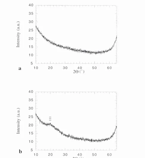
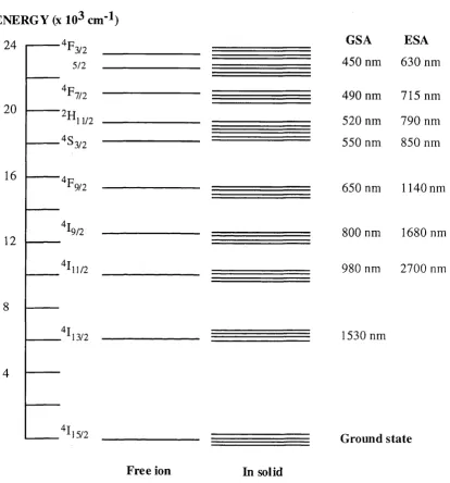
T h e A I2O3 th in film s d e p o s ite d by P E C V D d u r in g this r e s e a r c h p r o je c t w e r e a m o r p h o u s , as j u d g e d f r o m X - r a y d i f f r a c t o g r a m s , but a f t e r a n n e a l i n g at 1 0 0 0 °C f o r 2h a n d at 1 2 0 0 T fo r
5 h , t r a n s f o r m e d to p o l l y c r y s t a l l i n e Y-AI2O3 a n d a - A l2Û3 r e s p e c t i v e l y , as p r e s e n t e d in c h a p t e r 4.
2.3 Lattice Sites Of Er^+ In AI
2O
3R e c e n t s tu d ie s o f th e la ttic e sites o f Er3+ in s a p p h i r e [24, 2 5 ] , i n d ic a te th a t 7 0 % o f the E r
o c c u p i e s fre e o c ta h e d r a l sites (se e F ig u r e 2 .1 ), b u t d i s p l a c e d 0 . 8 Â f r o m th e ideal p o s itio n ;
2 0 % o f th e E r is in te tra h e d ra l sites, a n d th e r e m a i n i n g 10% is r a n d o m l y d is tr ib u te d . T h e s e
re s u lts s h o w t h a t in a - A l2 0], E r m a in ly o c c u p i e s f re e o c t a h e d r a l sites, w h i c h h a v e s im ila r s u r r o u n d i n g s as Al a n d E r h a v e in a - A l2 0g a n d E r2 0 3 c r y s t a l la t t i c e s , r e s p e c t i v e l y . M o r e o v e r , P L s tu d ie s o f b o th E r - i m p l a n t e d (X-AI2O3 a n d Y - A I2O3 s a m p l e s w ith th e s a m e a m o u n t o f o p tic a lly a c tiv e E r s h o w e d th at a p p r o x i m a t e l y 1 0 0 % o f the E r is o p tic a lly a c tiv e
in the s a p p h i r e s a m p le s . T h e r e f o r e , s in c e m o s t o f E r r e s i d e s on o c ta h e d r a l p o s itio n s , it c a n
b e c o n c l u d e d th a t E r in an o c t a h e d r a l s ite is i n d e e d th e l u m i n e s c i n g Er. O f c o u r s e th e
p o s s ib ility o f E r on tetra h e d ral o r r a n d o m p o s itio n s l u m i n e s c i n g c a n n o t b e e x c l u d e d [24].
T h e re s u lts o f this stu d y c an b e u s e d to e x p la in w h y h ig h a m o u n t s o f o p tic a lly a c tiv e E r c an
b e i n c o r p o r a t e d in A E G3. E r s h o u l d b e in th e t r i v a l e n t s t a t e in o r d e r to e x h i b i t th e c h a r a c t e r i s t i c r a d i a t i v e tr a n s i t i o n a r o u n d 1 .5 p m . In s a p p h i r e , A l a t o m s w h i c h o c c u p y
Chapter 2: Electronic & Optical Properties Of Rare-Earth Ions In Solids
Er occupies similar sites (free octahedral), implying that it is in the trivalent state in the lattice. As one out of every three octahedral positions in the AI2O3 lattice are unoccupied, the effective solubility of Er in AI2O3 is high, and high amounts of optically active Er can be incorporated. M oreover, octahedral positions in the AI2O3 lattice have a 6-fold coordination with O atoms. Other studies [25] have identified this surrounding for Er to be optically active.
These results not only explain the high solubility of Er in a - A l2 0 3 but the same conclusions hold for Y-AI2O3. The reason is that the hexagonal a - A l2 0 3 lattice and the cubic Y-AI2O3 lattice differ only in the stacking sequence of the O atoms, and have the same density of empty sites.
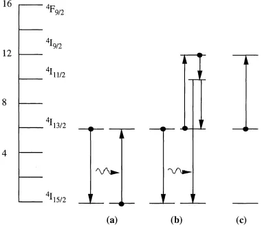
2.4 Energy Levels Of The Er+3 &
Yh^+
Ion
Figure 2.3 shows the energy diagram of Er^+ both as a free ion and when incorporated in a solid, for energy levels up to 24000 cm-^ [3, 4]. Figure 2.4 shows the energy levels of Yb3+ as free ion. In both figures the energy levels are labelled according to Russell- Saunders (LS) coupling. In this scheme the total orbital angular momentum (L) and the total spin (S) are vectorially added to form the total angular momentum (J) and the ion energy levels are labeled as ^s+iLj. Total orbital angular momentum is specified by the letters S,P,D,F,G,... which correspond to L = 0,1,2,3,4,...respectively.
The electronic structure of the rare-earth ions is dominated by electron-electron interaction with spin-orbit interaction immediately after in importance. The host material has the least influence [1-5]. The electron-electron interactions are caused due to Coulomb forces acting between the electrons in the unfilled 4f shells. The inter-Coulomb interaction splits the single electron configuration into a spectrum of states, whose energies depend on L and S, but not J. Spin-orbit interactions split the energy levels into multiplets by causing the energy of a state to be dependent on the total angular momentum quantum number J.
For rare-earth ions, the optical transitions from the infrared to the ultraviolet are between states composed of 4f wave functions. Because the initial and final states have the same parity, electric-dipole processes are totally forbidden and transitions for free ions can occur only by the much weaker magnetic-dipole and electric-quadrapole processes.
Chapter 2: Electronic & Optical Properties Of Rare-Earth Ions In Solids
electrons (4f) are situated inside the 5s^ and 5p^ shells and are therefore, to a certain extent, shielded from the ion's immediate environment.
ENERGY (x 10^ cm'^)
24
20
16
12
■4f
3/2
5/2
7/2
1/2
.4S3/2
■4f
9/2
9/2
4l11/2
4l
13/2
15/2
Free ion In solid
GSA ESA
450 nm 630 nm 490 nm 715 nm 520 nm 790 nm 550 nm 850 nm
650 nm 1140 nm
800 nm 1680 nm
980 nm 2700 nm
1530 nm
Ground state
Figure 2.3: E nergy le v e ls o f Er^+; for each state the G S A colu m n lists the w a v elen g th o f the ground state ab sorp tion (G S A ) transition term inating on it. T he E S A colu m n co n ta in s the w a v e le n g th o f the e x cited -sta te absorption (E S A ) transition to that le v e l originating on the \ -n2 m etastable le v e l [4].
C h a p te r 2: E lectronic & O ptical P ro p erties O f R are-E arth Ions In Solids
is t h e in itia l le v e l f o r p r o d u c i n g g a in at 1 . 5 3 p m . A n y p r o c e s s , a p a r t f r o m s t i m u l a t e d
e m i s s i o n , th a t r e m o v e s io n s f r o m th e m e t a s t a b l e le v e l c a n be c o n s i d e r e d as d i s s i p a t i v e ;
t h e s e p r o c e s s e s a re d i s c u s s e d in s e c tio n 2.6.
ENERGY ( x l0 3 c m - i )
1 2
5/2 1064 nm
2p7/2
O U
c
.2
Br
o CA
-O
<
Free ion
F ig u re 2.4: E n e rg y levels o f |2 , 4|.
0 . 5
0 . 4
0 . 3
0.2
4 0 0 600 800 1000 1200 1400 1600
W avelength (nm)
Chapter 2: Electronic & Optical Properties Of Rare-Earth Ions In Solids
2.5 Line Broadening Mechanisms & Radiative Transitions
In addition to splitting the energy levels, the crystal field can also affect the strength of the optical transitions between levels. The effect of the host on the rare-earth ions can be represented by a potential field which is usually expanded in a power series of spherical harmonics [1-4]. The even terms of the expansion slightly split the energy levels into Stark com ponents; the odd terms of the expansion induce a weak mixing of states (5d) of opposite parity to the 4f electrons, introducing a degree of electric-dipole strength into the intra-4f shell transitions i.e. make forbidden transitions allowed. This is a very important effect because most infrared and visible rare-earth transitions are dominated by this electric- dipole contribution; for the Er^+ transition though, from the ^I]3 /2 level to the "^I]5 / 2 state, the electric-dipole and magnetic-dipole transitions are comparable. The odd terms are only non-zero if the ion site lacks inversion symmetry, as it usually does in a glass or in an amorphous material. This means that rare-earth ions that occupy slightly distorted sites yield stronger fluorescent signals. In an amorphous material each individual ion occupies a unique site and the influence of the crystal field on each Er^+ ion is different. This translates to a variation of transition strength in a given Stark com ponent and results in inhomogeneous broadening of the emission spectrum.
The rare-earth transitions are also homogenously broadened; this is associated with the creation or annihilation of a phonon through the transition process between two energy levels. This process is temperature sensitive and it yields a characteristic thermal distribution of phonon energies which causes a spread of wavelengths for the absorption and emission. Spectral narrowing is achieved by a reduction in phonon population via a reduction in temperature. Phonon broadening acts on all the rare-earth ions to a similar extent and is thus homogeneous [1-4].
In a lightly doped medium (where the Er^+ ions are sufficiently far apart that each ion decays independently of all the other ions in the sample) an ion in an excited manifold can decay to a different manifold through any of the following processes: (1) spontaneous emission to any lower lying manifold, (2) multiphonon decay to the next lower lying manifold, (3) absorption/stimulated emission of a pump photon, and (3) absorption / stimulated emission of a lasing photon.
Chapter 2: Electronic & Optical Properties Of Rare-Earth Ions In Solids
quantum mechanical theory of rare-earth ion doped solid-state media, which allowed estimates to be made of the electric dipole transition strengths between any pair of LSJ manifolds. The Judd-Ofelt theory essentially involves using the line strengths of all the observable transitions from the ground state to excited manifolds, which can be determined from white light absorption measurements, and using these line strengths to estimate line strengths of transitions between pairs of excited levels. They proposed that the line strength between any manifolds i and j could be simplified to an expression of the form,
^ i j = Z A | ( 4 / " a [ ^ . ‘^ ] ./ ||c / ' ' i |4 / ”a ' [ L ' , S ' ] / ' ) f ( 2 . 1 )
t = 2 A , 6
where ^ 4 and are the Judd-Ofelt intensity parameters which characterise the strength and nature of the crystal field and |( 4 / ”o '[L ,5 ]/|f/^^ ^|4 /"a'[L ',5 '']7 ') are the squared reduced matrix elements which are essentially independent of the host material; their values, for most of the transitions of interest, can be found in the published literature. The theory has been used in the past with considerable degree of success (accurate to 10-
15%) which justifies the many approximations contained within the theory.
2.6 Multi - Ion Effects In Rare - Earth Doped Materials
As it was discussed in chapter 1, for an integrated rare-earth doped amplifier in an optical circuit on a chip, the length is restricted to several centimeters for any useful application. This im plies rare-earth concentrations in the range of 0.1-1 At%. At such high concentrations the distance between the rare-earth ions is small, and electric dipole-dipole interactions between the ions take place, the interaction strength of which depends on 1/r^, with r the distance between two rare-earth ions. As the doping density increases, there comes a point where the mean ion separation is sufficiently small that spatial migration of excitation from one rare-earth ion to a neighbouring ion becomes possible. Such transfer of excitation can be used to enhance the pumping of a laser transition and so increase the lasing efficiency (Forster transfer). However, there are other situations where multi-ion phenomena can impair laser performance. The following sections distinguish between the two cases, depending on whether energy m igration takes place between sim ilar or dissimilar rare-earth ions.
2.6.1 Like - Ion Interactions
Chapter 2: Electronic & Optical Properties Of Rare-Earth Ions In Solids
ion in the ground state. This results in a diffusion of the excitation and finally loss of the excitation if one of the Er^+ ions couples to a defect, for example, a hydroxyl group (OH ) [1, 29]. The energy transfer from the Er^+ ion to the OH complex serves as a trap and is extremely effective at quenching excited Er^+ ions [1, 29]. At high OH' concentrations this can occur through direct transfer from the excited ion. AI2O3 is known to have a strong catalytic effect, increasing OH' concentration. Although no chemical reaction occurs, it has the ability to immobilise many surface molecules because it has the appropriate structure to form weak links with H2O. OH' impurities can be easily reduced upon thermal annealing at 600°C; this effect is studied using Fourier transform infrared (FTIR) spectroscopy and is discussed in chapter 4.
16
12
9 / 2
9 / 2
1 1 / 2
41,
IL
v w
‘^ h 5 / 2 'r \ r
(a)
1A / W
(b)
(c)
Figure 2.6: S ch em atic o f three different concentration quenching e ffe c ts in Er^+ (a) energy m igration, (b) coop erative u p-conversion and (c) excited-state absorption (E SA ). The left hand side scale sh o w s the Er^+ energy le v e l diagram w ith the corresponding R ussell-Saunders notation [28].
Chapter 2: Electronic & Optical Properties Of Rare-Earth Ions In Solids
decays rapidly to the ^ I n/ 2 level through a non-radiative transition by emission of phonons. From there it can either decay back to the metastable level (^1 1 3/2) or to the ground state. As a result, cooperative up-conversion reduces the degree of inversion at a given pump power. The rate of cooperative up-conversion depends quadratically on the concentration of ions in the "^Ii3 / 2 state [28],
Very efficient cooperative up-conversion can occur when two or more Er^+ ions form ion- pairs (clusters), resulting in almost immediate interaction of the ions once both of them are excited. This form of interaction is called pair-induced quenching (PIQ) [28, 30-33], and effectively limits the maximum degree of inversion attainable in the material.
In the energy levels of the lanthanide ions, there is the possibility of accidental degeneracies existing, where the spacing of two excited energy levels matches exactly the energy of either the pump or the lasing photons. Therefore, up-conversion can also occur by the excitation of an ion in the metastable '^1 1 3 / 2 state to a higher level through the absorption of a pump or signal photon. Even if the ion ultimately returns back again to the upper lasing level, a photon will be lost either to heat or spontaneous emission. This effect is called excited-state absorption (ESA) and reduces the pumping efficiency. Figure 2.6(c) shows ESA when pumping at 800nm; an Er^+ ion in the "^Ii3 / 2 is promoted to the ^1 9 /2 state by the absorption of an 800nm photon. Excited ions have an ESA spectrum which differs from their GSA spectrum due to the new energy gaps in the higher lying states. This is shown in Figure 2.3 where each state above the "^Ii3 / 2 is labelled with the wavelength of the ESA transition terminating on it [4]. ESA depends on the concentrations of Er^+ ions in the 4I]3 / 2 level as well as on the pump intensity.
Although up-conversion processes put a limit to the performance of the optical amplifiers operating at 1.5|Lim, they may be used to create higher-energy excitations, and thus shorter- w avelength photons, using relatively long-w avelength pump light. One of the characteristics of ESA is the observation of fluorescence at shorter wavelengths than the pump [28]. For example ESA promotes ions from the '^Ii3 / 2 to the % n/ 2 state (pumping at 800nm); from there the ions can either decay non-radiatively back to the ^Ii3 / 2 level or decay radiatively to the ground state emitting at 520nm, 550nm or 650nm [4, 28].
Chapter 2: Electronic & Optical Properties Of Rare-Earth Ions In Solids
(YAG), which has a similar crystal structure as AI2O3, has a Cup=5.4xl0'^'^ cmYs much higher than AI2O3. For soda-lime silicate glass, Cup=3xlO-^^ cm^/s, nearly the same as AI2O3. Recent studies of two other silica-based glasses show that Cup=l-10xl0-^^ cm^/s [28].
2.6.2 Co - Doping
The idea of deliberately incorporating two or more types of rare-earth ion simultaneously into a medium has been in existence for a long time. Figure 2.7 shows the most common use of co-doping. The laser transition of interest takes place between two levels of the acceptor ion. The donor ion is there to absorb the pump radiation. Following the absorption of a pump photon, a donor ion relaxes from the pumped level down to a metastable level. If the fluorescence from that metastable level overlaps with the absorption spectrum of the acceptor ion, and if the acceptor ion density is sufficiently high, then there is a distinct probability that a donor-acceptor pair will undergo a radiationless transition leaving the donor ion back in the ground state and pumping the acceptor ion to an excited level.
Donor
Acceptor
Lasing
Transition
Pump
Transition
Figure 2.7: Sch em atic energy lev el diagram sh ow in g h o w energy transfer betw een donor and acceptor ion s (dashed lin es) can lead to a population inversion in the acceptor su b system [2].
C h a p te r 2: E lectro n ic & O ptical P ro p erties O f R are-E arth Ions In Solids
th e p u m p i n g w a v e l e n g t h th e r e are p u m p e x c i t e d - s t a t e a b s o r p t i o n p r o b l e m s th a t n e e d to be
a v o i d e d . T h i s is i n d e e d th e c a s e w ith Er^+ w h i c h s u f f e r s f r o m E S A (e.g. a t SOOnm) as
d i s c u s s e d in s e c tio n 2.6.1.
3 C O
4—»
Dh Ch
o
c/2 X)
<
0
000
1 0 0
6 0 0 8 0 0 1 0 0 0 1 2 0 0 1 4 0 0 1 6 0 0
Wavelength (nm)
F ig u re 2.8: A bso rp tio n sp ectru m o f an Yb^+/Er^+ SiOz optical fibre [35].
T h i s r e s e a r c h w o r k w a s c o n c e r n e d w ith c o - d o p i n g th e E r3+ :A l2 0 3 s y s t e m w ith Yb^+. In this c a s e , Yb^+ io n s a re th e d o n o r a n d th e Er^+ io n s the a c c e p t o r . A s m a ll Er^+/Y b3+ io n -
ion s e p a r a t i o n p r o v id e s a v ery e f f ic ie n t in d ire c t p u m p i n g m e c h a n i s m f o r Er^+ a n d m a y also
a llo w d o p i n g w ith e x t r e m e l y h ig h Er^+ c o n c e n t r a t i o n s w i t h o u t s e r io u s r e d u c t i o n o f g a in o r
p u m p d u e to c o o p e r a t i v e a n d p a i r - i n d u c e d u p - c o n v e r s i o n [34]. W i t h o p t i m i s e d r a r e - e a r t h
c o n c e n t r a t i o n a n d f a b r i c a t i o n p r o c e s s , th e f o r m a t i o n o f Er^+ZEr^^ i o n - p a i r s m a y b e
c o m p l e t e l y e l i m i n a t e d a n d e a c h E r^+ ion c a n b e c o n s i d e r e d c l u s t e r e d o n l y to th e
s u r r o u n d i n g Yb^+. In s u c h a c o n d i t i o n , the h a r m f u l e f f e c t d u e to p a i r - i n d u c e d q u e n c h i n g
f r o m t h e Er^+ m e t a s t a b l e lev el is c o m p l e t e l y e l i m i n a t e d a n d , at th e s a m e t i m e , a v e r y
e f f ic ie n t e n e r g y tra n s f e r p r o c e s s ( in d ire c t p u m p i n g ) f r o m Yb^+ to Er^+ e f f e c tiv e ly c o n t r a s t s
c o o p e r a t i v e u p - c o n v e r s i o n . It h a s b e e n r e p o r t e d t h a t w i t h i n c r e a s i n g t h e Y b ^ +
c o n c e n t r a t i o n , Yb^+ to Er^+ e n e r g y t r a n s f e r p r o g r e s s i v e l y r e d u c e s th e n e g a t i v e e f f e c t o f
Ei'3+ i o n - i o n in te r a c tio n s at h ig h Er^+ c o n c e n t r a t i o n s . A t l o w e r Er^+ c o n c e n t r a t i o n s , th e up-
c o n v e r s i o n p r o c e s s e s d o n o t s e rio u s ly a ffe c t a m p l i f i e r p e r f o r m a n c e a n d th u s the a d d itio n a l
![Figure 1.1: (a) A schematic of an EDFA and (b) the three level lasing system provided by Er^+ [10].](https://thumb-us.123doks.com/thumbv2/123dok_us/8616278.1405986/16.597.35.531.65.604/figure-schematic-edfa-b-level-lasing-provided-er.webp)

![Figure 3.1: The thin film formation [7],](https://thumb-us.123doks.com/thumbv2/123dok_us/8616278.1405986/52.597.91.531.110.586/figure-the-thin-film-formation.webp)