Systems
GA33-1526- 2 File No. 4300-01
IBM 4331 Processor
Functional Characteristics
and Processor Complex
Configurator
- - -
-- -- -- --
-
- - - -
-
_._._-- .
.---- .----
-
----
Third Edition, June 1980
This major revision of IBM 4331 Processor Functional Characteristics and Processor-Eomplex Configurator
obsoletes the second edition, GA33-1526-1. Information is added on the 4331 Processor Model Group 2 and on new DASD
compatibility features. Other sections of the manual have
been brought up to date.
Requests for copies of IBM publications should be made to your IBM representative or to the IBM branch office serving your local i ty.
It is possible that this material may contain reference to, or information about, IBM products (machines and programs), programming, or services that are not announced in your country. Such references or information must not be construed to mean that IBM intends to announce such IBM products, programming, or services in your country"
A form for reader's comments is provided at the back of the publication. If the form has been removed, convnents may be addressed to IBM Product Publications, Department 3179, Schoenaicher Strasse 220,7030 Boeblingen/Wuertt., Federal Republic of Germany. IBM may use or distribute any of the
information you supply in any way it believes appropriate without incurring any obligation whatever. You may, of course, continue to use the information you supply.
C Copyright International Business Machines Corporation 1979, 1980
Preface
Page of GA33 - 1526 - 2
Revised September 15, 1980
by TNL GN33 - 1733
The characteristics of the IBM 4331 Processors with their I/O adapters, standard channels and data communication
facilities are described ~n this publication for the use of
sytem analysts and programmers.
The reader is assumed to have a working knowledge of the IBM 4300 Processors Principles of Operation for ECPS:VSE Mode, Order No. GA22-7070, and the IBM System/370
Principles of Operation, GA22-7000, and to have had programming experience with System/360, System/370, or other 4300 Processors.
Note: The term "principles of operation manuals" used in this publication refers to the two manuals listed above.
The main chapters of the manual cover: • Introduction to the 4331 Processor
• 1/0 and data communication characteristics • ~odel-dependent information
• Compatibility features
Appendixes present a calculation of available processor storage, machine instruction timings, definitions of the abbreviations and special terms, and code tables for the communications adapter.
Prerequisite Reading
IBM 4300 Processors Summary and Input/Output ~ Data
-Communications Configurator, GA33-1523
Associated Publications
IBM 4300 Processors Installation Manual-Physical Planning, GA24-3667
IBM 4331 Operating Procedures and Problem Determination Guide, GA33-1525
~331 Processor Channel Characteristics, GA33-1527 IBM 4331 Processor Compatibility Features GA33-1528 IBM 3270 Information Display s*stem
Component Description, GA27-27 9
IBM 3289,Model
E
Printer Component Description andOperator s Guide, GA27-3159
IBM 3262 Printer Models 1 and 11 Component Description,
GA24-3733 - -
Page of GA33 - 1526 - 2 Revised September 15, 1980
by TNL GN33 - 1733
t
IBM 8809 Magnetic Tape Unit Introduction, GA26-1659
IBM 3310 Direct Access Storage Reference Manual, GA26-1660
IBM 5424 and ~ Multifunction Card Units Operator's Guide
and Programmer s Reference Manual, GA21-9167
IBM 4331 Processor: DASD Adapter for 3370 Direct Access Storage: Reference Manual, GA33-1539
IBM 3540 Diskette Input/Output Unit Operator's Guide and Programmeris Reference, GA21-9197
IBM 4331 Processor Loop Adapter Functional Characteristics GA33-1534
Illustrations
Figure Title
1. IBM 4331 Processor with Input/Output Devices
2. Simplified Processor Data Flow (4331 Model Group 1) 2-1
3. Simplified Processor Data Flow (4331 Model Group 2) 2-2
4. Storage Concept 2-4
5. Processor, Main Elements 2-5
6. 3278-2A Display Console 2-7
7. Operatorls Control Panel 2-8
8.
Console Keyboard 2-109. Integrated Channel, 4331-1 3-1
10. Integrated Channel, 4331-2 3-2
11. Support Subsystem 3-12
12. I/O Subsystem 3-14
13. DASD Adapter and 8809 Magnetic
Tape Unit Adapter 3-15
14. Standard Channel Adapter 3-18
15. Structure of Communications
Adapter 7-2
16. Line Control Sequence for IBM
Terminal Control-Type 1 with
1050 Data Communication System 7-9
17. Line Control Sequence for IBM
Terminal Control-Type 1 with
1060 Data Communication System 7-10
18. Line Control Sequences for IBM
Terminal Control-Type 1 with
2740 Communication Terminal 7-11
19. Line Control Sequences for IBM
Terminal Control-Type 1 with
2741 Communication Terminal 7-12
20. 4331-1 Configurator 10-1
21. 4331-2 Configurator IAI 10-3
22. 4331-2 Configurator IBI 10-5
23. 4331-2 Configurator ICI 10-7
24. Code Structure for 1050
Data Communication System 0-1
25. Code Structu~e for 1060 Data
Communication System 0-2
26. Code Structure for 2740 and 2741
Communication Terminal 0-3
27. EBCDIC as used for Binary
Synchronous Communication
Control 0-4
28. ASCI I as used for Binary
Synchronous Communication
Control 0-5
CONTENTS
Chapter 1. Introduction . . Relationship to System/370 Compatibility . . . . Programming Support . . . . .
· . 1-1 . . . 1-1 · . 1-2
1-2 Processor Configuration and Features.
Maintenance Concept . . . • . Remote Support Facility . . . .
· . 1-3 . 1-3 · . 1-3
Chapter 2. System Structure . . Machine Summary . . .
Storage. • . . . . Storage Features . • • • • . High Speed Buffer Storage . . Processor • . . • . . .
· . 2-1 · . 2-3
· . . . 2-3
· . . . 2-
3
· . 2-4 · . 2-5
IBM 3278 Model 2A Display Console. · . 2-7
Contro 1 Pane 1 •
Keyboard . . . Display Screen. System Operation
· . 2-8
. 2-9
· . 2-15 • . . • . . 2-16
Chapter 3. I/O Adapter Characteristics . . 3-1
Integrated Channel . . . 3-1
Input/Output Adapters . • . . . • . . . 3-4
Channel and Device Addresses . . . 3-5
Support Subsystem . . . • . . . 3-11
I/O Subsystem. . . . . . . . . 3-14
Chapter 4. Keyboard/Displays and
Terminal Printers . . 4-1
3270 Commands. . . .' • • . . 4-1
'Wr i t e' Comma n d, Hex '0 1 ' . . . 4 - 2
'Erase/Write' Command, Hex '05' • . • . . 4-3 'Erase/Write' Alternate, Hex '08' . . . . 4-4 'Erase all Unprotected' Command Hex 'OF' 4-4 'Read Modified' Command, Hex '06' . • . . 4-5 'Read Buffer' Command, Hex '02' . . • . . 4-7
'Sense' Command, Hex '04'. . • . . . 4-7
'Sense I/O' Command, Hex 'E4'.. ..4-7
'N o operation, ex . , H '03' . . . . . . -4 8
Orders and Control Characters . . . 4-8 Write Control Character . . . 4-8 'Set Buffer Address' Order, Hex '11' . . 4-10
'Start Field' Order, Hex '10'.. . . 4-11
Attribute Character. . . 4-11
, NL " Hex I 15' :. . . 4-13
'EM', Hex '19':. . . 4-14
'FF', Hex
'oct:. . . .
.
4-14, Ins er t Cur so r' 0 r de r, Hex '1 3 '. . . 4 - 14 'Program Tab' Order, Hex '05' . . . 4-14 'Repeat To Address' Order, Hex '3C' . . . 4-15 'Erase Unprotected To Address' Order,
Hex '12'. . . 4-15
Display Status . . 4-17
Unit Status. . . 4-17
Channel Status . 4-19
Video Display Sense Information. . . 4-20
Sense Byte 0 . . . • . . . 4-20
Visual Status Indicators . . . . . . 4-21
1052 Commands . . . 4-21 'Write Inhibit Carrier Return', Hex '01' 4-22 'Write Auto Carrier Return', Hex '09' . . 4-23
'Read Inquiry', Hex lOA' . . . . . 4-24
, Contro 1 No-Op', Hex '03'. . . 4-26
, Con t r 0 1 A 1 arm', Hex '0 B '. . . 4 - 26
, Sense', Hex '04'. . • . . . . 4-26
'Sense 1/0', Hex 'E411. . . . 4-26
Console Printer Status. . . . . 4-27
Unit Status. . . 4-27
Channel Status . . . • . . . . 4-28
Console Printer Sense Information.. . 4-29
Sense Byte 0 . . . 4-29
Chapter 5. Diskette Drive. 5-1
Commands . . . . . . . . 5-1
Define Operations (2F) . . . 5-1
Seek (07). . . . . . 5-4
Read I PL (02). . . . 5-6
Read Data (06) . . . . . . 5-6
Write Data (05). . . . . 5-8
No Operation (03). . 5-9
Write Control (21) . 5-9
Sense (04) . . . . . . . 5-10
Sense I/O (E4) . . . . . . 5-11
Feed (17). . . • . . . . . 5-11
Diskette Drive Reset States. . . . . 5-11
Manual Operations. • . . . 5-12
Diskette Unit Status . . . 5-13 Diskette Sense Information . . . 5-14
Error Definitions. . . • . . 5-18
Visual Error and Status Indications . . . 5-19
10 Errors During Read or Write . . 5-19
Read or Write Data Errors. . . . . . 5-21
Chapter
6. 3340/3344
Direct Attachment • .6-i
Commands and Instructions. . .
6-1
Status Information . . . . • . . .
6-3
Sense Information. . .
6-4
Chapter 7. Commun i cat ions Adapter.. . 7-1
IBM Terminal Control - Type 1. .
7-3
Line Control Characters. .
7-4
Transmission Code. . . . . 7-5
Commands . . . . . . 7-5
Unit Status. .
7-17
Sense Information. . 7-18
Binary synchronous communications control.
7-24
Line Control Characters. . . . .
7-24
Transmission Code.
7-26
Commands . . . . • .
7-27
Unit Status. . . . • . . . 7-38
Sense I nformat ion. . . . . .
7-40
Synchronous data 1 ink contro 1 . . 7-45
Commands . . . . • . . .
7-47
Basic Commands. . .
7-47
High-level Commands. . . .
7-55
Station Control Block. .
7-55
High level commands. . . .
7-60
Channel Program Rules. . . . . . .
7-70
Channel Program Examples .
7-70
Status Information . . . . . . .
7-74
Unit Status. . . • .
7-74
Channel Status . . . . • 7-76
Sense Information.
7-77
Sense Bytes 0 and 1 . . . • . . . 7-78
Sense Bytes
2
and3. . .
. . . . 7-84
Sense Bytes
4-23 . . . .
7-84
Soft Errors and Recovery . . • .
7-84
CCW Flags. . .
7-86
Termination of Operations. . . •
7-87
Interruptions. . .
7-88
Ending Condition Classification.. .
7-89
General Synchronization Rules . . .
7-90
Line Direction Transitions. . . . .
7-90
Channel Program Synchronization Rules . .
7-90
Description of Timeouts. . . 7-91
Nonproductive Receive Timeout. . .
7-91
Idle Detect Timeout. . . 7-92
Fill Character Timeout. . • . .
7-92
Unit Check and Soft Error Handling..
7-93
Dynamic Trace Feature. . . . . . 7-93
Trace Analysis. . . . 7-94
Trace Channel Commands . . . . .
7-94
Chapter
8.
Model-Dependent Information . .8-1
Channels • . . . 8-1
. 8-1
Implementation . . . Limited Channel Logout. Channel Logout Recording Partial Results . . .
. . . . 8-1
vii i 4331 Functional Characteristics
. . . 8-3
Controls . . . . • . · . 8-4
Clock Resolutions. Instructions . . . .
. . . 8-4
Manual Operations . .
Specifying Storage Address . . Power-On State . . . . Program Event Recording . . Machine Check Handling . . .
Control Register 14 . . . .
Machine Check Interruption Code. Machine Check Recording • .
· . 8-4 · . 8-4 · . 8-6 · . 8-6 · 8-6 · . 8-6 · . 8-6 · 8-8
· . 8-11 Storage. . . .
Reference and Change Recording.
· . 8-11 . . . 8-11
Chapter 9. Compatibility Features. . . 9-1
Direct Access Storage Compatibility . .
Feature • . . . 9-1 1401/1440/1460 Compatibility Feature • . . 9-2
System/3 Data Import . . . . . . . 9-3
Chapter 10. 4331 Processor Complex
Configurator . . . . . . 10-1
Standard Functions.
Optional Features . . .
Appendix IAI. Calculation of Available Processor Storage . . . . .
Table AA . . . . Table AA1 . . . . .
· .10-9 · 10-10
· A-1 · . A-2 · . A-3
Appendix IBI. Instruction Timings . . . B-1
Processor Performance. . . . . B-1
4331 Model Group 1 . . . . B-4
legend . . . • . . . . . B-10
Special Instructions. . . . . . . B-11
Move Inverse (MVC IN) . . . . B-11
MVCIN D1(l,B1), D2(B2) . B-11
Resolution of Average Values . . . B-12
ClM-Timing (in micro sec). . . . B-12
STCM Timing (in micro sec) . . . B-13 SlA Timing (in micro sec) . . . B-13
SRA Timing (in micro sec). . . B-13
SRDA-Timing (in micro sec) . . . B-14
SlDA-Timing (in micro sec) . . B-14
AP, SP Timing (in micro sec) . B-14
CVD Timing (in micro sec). . . . . . B-14
MVC Timing (in micro sec) . . . B-15
XC Timing (in micro sec) • . . B-16
ZAP Timing (in micro sec) . . . B-16
433 1 Mode 1 G roup 2 . . . B - 17
Appendix IC I . Definitions. . . . . C-1
Glossary of Terms and Abbreviation . C-1
Appendix IDI. CA Code Tables. . . . . D-1
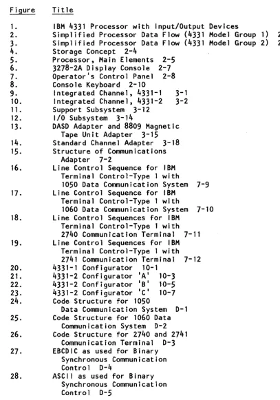
[image:9.615.72.560.48.738.2]Figure 1. 1 BM 4331 Processor with 1 nput/Output Devices
Chapter 1. Introduction
Page ofGA33 -1526- 2 Revised September 15, 1980
by TNL GN33 - 1733
The IBM 4331 Processor (Figure 1) is a compact general
purpose data processor designed to give new standards of performance and simplicity in small-to-medium sized applications. Its concept includes:
• Ease of installation, with minimum disturbance of
existing input/output (I/O) configurations.
• Reduced processor time on certain frequently-used functions, provided in ECPS;VSE mode.
• Selectable System/370 mode.
• Compatibility features for easy transfer from System 3,
System/360, System 370, 1401/1440/1460-Series, and from ex'i st Ii ng to new DASD.
• I/O adapters for direct connection of teleprocessing
lines and selected input/output devices.
• Standard channels for 4300, System/360 and System/370 input/output devices.
• DASD adapter and magnetic tape unit adapter. • Multiuse communications loop adapter.
• Internal processing speed reaching 200,000 machine
instructions per second (Model Group 1) and 420,000 machine instructions per second (Model Group 2).
ReladoDsbip to SysteDl/370
The 4300 Processors are a further development of the Systeml370. The non-privileged instructions in the two systems are i dent i cal. The rna in difference in the 4331 is the simplified dynamic address translation (one-level address translation) which uses only one table to generate an address from a storage of up to 16,777,216 bytes.
A further simplification in the 4331 processors is that storage addresses for I/O operations are also handled by the address ttanslation. This concept of address
translation is supported under DOS/VSE by new privileged . instructions which allow the storage blocks to be
controlled with less overhead. This mode of operation is called ECPS:VSE mode.
The more complex dynamic address translation of the System/370, which allows multiple virtual storages to be created, is available in the 4331 Processors at the
selection of the operator. This mode of operation is called System/370 mode.
Compatibility
Any program written for the 4300 Processors operates on a 4331 provided that it:
1. Is not time-dependent.
2. Does not depend on system facilities (such as storage
capacity~ I/O equipment~ or optional features) being present when the facilities are not included in the configuration.
3. Does not depend on system facilities being absent when
the facilities are included in the 4331. For example~
the program must not depend on interruptions being caused by operation codes not installed in some processors but installed in the 4331.
4. Does not depend on results o~ functions that are
defined in the principles of operation manuals (see 'Preface') to be unpredictable or processor-dependent.
5.
Does not depend on results or functions that aredefined in this publication to be deviations from the principles of operation. See the chapter entitled
• 'Model-dependent Information" for a description of
the deviations.
Any program written for System/370 or System/360 operates on a 4331 in the System/370 mode, provided that the program follows the preceding rules and, if written for System/360, does not depend on functions that differ between System/360 and System/370.
For more details about compatibility, see the IBM 4300 Processors Principles of Operation for ECPS:VSE Mode, GA22-7070.
Programming Support
The 4331 runs under the following operating systems:
• DOS
• DOS/VS
• DOS/VSE
• OS/VS1
• VM/370
Please refer to your IBM representatiye.for the appropriate
release numbers. The one-level addressing described above
is supported only in ECPS:VSE mode. More information on programming support is given in programming publications.
Processor Configuration and Features
The processor configuration and features are shown in the final chapter of this manual, 114331 Processor Complex Configurator " . For details of local and remote I/O configurations see IBM 4300 Processors Summary and
Input/Output! Data Communications Configurator, GA33-1523.
Maintenance Concept
The maintenance of the 4331 Processor is based on reference codes displayed on the operator's console and logged on the system diskette for later retrieval by the service
representative. Each reference code leads the service
representative to a specific procedure for replacing a failing unit. The reference code is automatically generated from the failure symptoms developing in the machine.
Remote Support Facility
This facility (with customer authorization) permits the 4331 to be controlled from a remote IBM site and gives the on-site service representative access to the latest service aids and information.
With this mode, the IBM remote support representative can perform online diagnosis as though he were at the
customer's site. Logout data stored on the system diskette can be saved during the data link operation for offline analysis. Microcode patches may also be applied remotely.
The remote connection is supplied by the customer. For
details of the customers's responsibilities, see IBM 4300 Processors Installation Manual-Physical Planning,--- ----GA24-3667.
The operator IS console is used as a control monitor to
check the content of data to be transmitted. A line disc~nnect key is provided for the customer to stop data transmission immediately.
Page of GA33 - 1526 -2
Revised September 15, 1980
by TNL GN33 - 1733 2. System Structure
CTLI
CTLI
TP Lines
Standard Interface
l=
1=
F
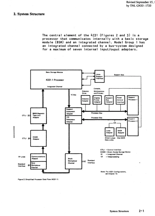
The central element of the 4331 (Figures 2 and 3) is a
processor that communicates internally with a basic storage module (8SM) and an integrated channel. Model Group 1 has an integrated channel connected by a bus-system designed for a maximum of seven internal input/ouput adapters.
Basic Storage Module ...
Units Support Bus
wr
Support4331-1 Processor Interface
Integrated Channel
Console,
1
~ ~ Diskette Workstations
Drive and Printers IC Bus
Diskette Display Support Power Support Adapter Printer Bus Control Processor 1
Adapter Adapter Interface
"
~I
I
I
I
Support
..
Subsystem .... ....
8809 Magnetic Adapter Processor Bus
Tape Unit
Adapter I/O
....
Processor Bus ....Subsystem Support
Adapter ... I ... Processor 2
f
r-0R~ i-Loop 5424 Adapter Adapter
DASD Direct Loops One 5424
Adapter Data Links
CTLI = Control Interface
,
,
DASD = Direct Access Storage Device IC = Integrated ChannelCommunications TP = Teleprocessing
Adapter Block
Multiplexer
F==t Standard
Bvte Channel Interface "'
Multiplexer C",nnel
•
I Note: For 4331 Configurations, [image:15.613.49.571.46.774.2]see Chapter 10.
Figure 2. Simplified Processor Data Flow (4331·1)
Page of GA33 - 1526 - 2 Revised September 15, 1980
by TNL GN33 - 1733
CTLI or Standard Interface CTLI or Standard Interface
TP Lines
Standard Interface
l=
1=
F
Model Group 2 has an extended integrated channel connected by two bus systems designed for a maximum of eight internal
input/output adapters. The number of adapters installed
depends on the processor configuration. Each adapter
controls a subsystem, provides an interface, or satisfies the demands for input/output placed on a modern data processing system.
Basic Storage Module
Units Support Bus
~
Support4331-2 Processor Interface
I ntegrated Channel
~ ~ A ~ Console,
1
Diskette WorkstationsIC Bus IC Bus Drive and Printers
Diskette Display Support Power Support Adapter Printer Bus Control Processor 1
Adapter Adapter Interface
,
,
_1
1I
I
8809 Magnetic Support
..
Tape Unit Subsystem ~
Processor Bus ...
Adapter or Adapter
Block I/O
Multiplexer """'- Processor Bus
Subsystem
..
SupportChannel
Adapter .... I
...
Processor 2~R§j
t
l
,-DASD Loop 5424
Adapter Adapter Adapter
or
DASD High Speed
Adapter ~ CTLI Direct Loops One 5424
Block Data Links
Multiplexer Channel
CTLI = Control Interface DASD = Direct Access Storage Device IC = I ntegrated Channel
Communications TP = Teleprocessing
Adapter Block
Multiplexer ~ Standard
Byte Channel Interface
Multiplexer Channel
•
I
[image:16.618.76.531.221.601.2]Note: For 4331 Configurations, see Chapter 10_ Figure 3. Simplified Processor Data I=low (4331-2i
Machine Summary
The basic characteristics of the 4331 are:
BSM size BSM type
"BSM refresh rate BSM refresh duration BSM access width BSM read cycle BSM write cycle Data flow width Instruction buffer
Translation look-aside buffer High-speed buffer storage RCS size
RCS type
RCS refresh rate RCS refresh duration Control buffer size
Model Group .1
0.5 or 1.0 megabytes Single-cell
11.2 usec 1.0usec 4 bytes
0.9 usec(4 bytes) 1.3 usec (4 bytes) 4 bytes
16 bytes
2-way, 32 entries None
64 or 128 kilobytes Dual cell
50 usec 400 nanosec 64 bytes Control buffer access time 100 nanosec Control word size 4 bytes Read-only store None
Number of standard channels 2 (maximum)
Speed of byte MPX (byte/burst) 18/500 kilobytes/sec Speed of block MPX 0.5 megabytes/sec Speed of high-speed block MPX Not applicable Number of internal I/O adapters 7 (maximum) Service subsystem
BSM Basic storage module IC Integrated Channel
Res Reloadable control storage MPX
=
MultiplexerStorage
~odel Group
a
1,2,3 or 4 megabytes Single-cell
19.2 usec 1.0 usee 16x4 bytes
2.6 usec (64 bytes) 3.1 usec (64 bytes) 4 bytes
None
2-way, 32 entries 8 kilobytes
128 kilobytes Dual cell 50 usee 400 nanosec 64 bytes 100 nanosec 4 bytes 12 kilobytes 4 (maximum)
18/500 kilobytes/se~
1.25 megabytes/sec 1.86 megabytes/sec 8 (maximum)
The storage (Figure
4)
consists of up to 16,777,216 bytes,of which 0.5 to four megabytes, depending on the
4331
model, are processor storage (see configurator in chapter 10). The processor storage is a basic storage module (BSM) that is part of the processor and is controlled by it. There is no separate storage control unit. In Model Group
1, bytes of information are fetched in groups of
4,
16, or32, and stored in groups of
4,
as determined by theprocessor microcode. In Model Group 2, the bytes are
fetched in groups of 64 into a high-speed buffer storage
(see following description) and are also stored from this buffer in groups of 64. The 8SM communicates with the processor over a 4-byte bus used for transferring commands, addresses, and data in both directions.
Depending on the feature configuration, part of the 85M is occupied by microcode and is therefore not available to the user. See the descr i pt i on of microcode under Ilprocessoril in this chapter.
Virtual Storage ( 1, 2, 4, 8, or 16 megabytes)
Processor
I
Extern. IStorage \ DASD Storage
'-~~---~
[image:18.621.51.527.200.352.2]... _ - /
Figure 4. Storage Concept
Storage Features
The 85M has single-bit error correction within four bytes (Model Group 1) or within eight bytes (Model Group 2), and double-bit error detection.
High-speed Buffer Storage (Model Group 2 Only)
The Model Group 2 has eight kilobytes of high-speed buffer storage between the 85M and the processor. This buffer storage accelerates the traffic to and from the processor and compensates for the relatively slow access of the 85M. To the processor, the high-speed buffer storage is the
location from which all instructions and operands are fetched (at 200 nanoseconds per word). The high-speed buffer is also the location where all results are stored. When the desired information is not found in the buffer storage, the 85M is signaled to supply a further 64 bytes of information. A corresponding group of the 64
least-recently used bytes is then either overwritten (or stored back in the 85M and overwritten) by the incoming bytes. Only data changed during processing is stored back.
Processor
The processor is microcode-controlled and has a data flow
four-bytes wide. Its main elements are shown in Figure
5.
The time for executing a microinstruction varies from 200 nanoseconds (Model Group 2) or 300 nanoseconds (Model Group
1) to 1.6 microse~cnds depending on the complexity of the
operation. A microinstruction which addresses processor storage may take up to four microseconds.
To 1/0 - - - . Adapters .... ~I----II
Integrated Channel (s)
.---T---~
+
Data Local Store
Processor Storage
t
I
AlignerTranslation Look Aside Buffer
l
System/370Instruction Buffer
Key Storage Manual Operations
r+
I
I I
Control Storage
~,. I
1--_______ ... "'-... _ _ _ ... _ _ _ - - - - ___ J
,,.
,
\
Arit~metic
7
Logic Unit
..
...Figure 5. Processor, Main Elements
~,
Support Hardware
Op-Register
To Processor Control Points
[image:19.617.134.569.228.630.2]The microcode executes the machine instructions defined in the principles of operation manuals, including input/output
instructions and commands. In Model Group 1 up to eight
trap levels handle the various logical and input/output tasks according to fixed priorities. The processor operates on a ninth level which has the lowest priority. Model Group 2 has two entries per trap level, giving in effect sixteen levels, plus a seventeenth for the
processor.
The microcode resides in a reloadable control storage located in the processor. Model Group 2 has 128 kilobytes of reloadable control storage and Model Group 1 has 64 bytes or 128 kilobytes, depending on the configuration. Model Group 2 contains additional microcode in a read-only storage. The microcode is loaded from the system diskette at IML. None of the reloadable control storage is available
to ,the user. Microcode that exceeds the limit of this
storage is located in a protected area of processor storage. This code is mainly for handling machine checks and exceptional conditions; it consists partly of UCWs and other control information which is not constantly used. When required, the code is fetched by an automatic
mechanism. The processor storage reserved for microcode
depends on the system configuration. To determine the processor storage available to the user, see Appendix IAI.
When microcode from reloadable control storage is to be used, sixteen microwords at a time are read into a buffer to counteract the effect of access delay. When microcode from processor storage is to be used, eight microwords (Model Group 1) or four microwords (Model Group 2) are read at a time into the same buffer. An address compare network determines if the code needed is in the buffer, in the reloadable control storage, or in the processor storage. The microinstruction addresses are then routed accordingly.
The processor hardware consists of a fullword (4-byte) arithmetic and logic unit, a fullword shift unit, two kilobytes of local storage, an additional 128-byte local store (Model Group 2 only), and hardware for address decoding, floating-point acceleration, and condition code generation. The local storage provides space for the work registers needed for addressing and accumulating the
results of operations. It also holds the general registers, floating point registers, control registers, and most of the UCWs for the transfer of channel data. The additional
local store in Model Group 2 contains a duplicate of the general purpose registers. Duplication allows two register operands to be fetched simultaneously, thus saving an access cycle and increasing the speed of processing.
The processor converts instruction and operand addresses to addresses in processor storage before processing. The
conversion is done through a table in a protected area of processor storage. To avoid using this table for every reference, the processor keeps a copy in a translation look-aside buffer (TlS). The TlB holds the virtual
addresses and corresponding BSM addresses equivalent to
64
pages (a total of 128 kilobytes), and is capable of rapid conversion. When an address that is not stored in the TlB
is referenced, a microcode trap occurs and the TlB is updated. Information passing to or from BSM is adjusted by aligners which compensate for the fixed access width of four bytes.
IBM 3278 Model 2A Display Console
The 3278-2A Display Console (Figure 6) is an input/output
device used for communication between the system and the operator. It consists of a keyboard, a display and a
control panel. Operator commands and console messages allow interaction between the operator, the operating system, and the processor hardware. For instance, the operator may receive a message from the operating system that an
input/output device needs attention.
Figure 6. 3278 Model 2A Display Console
Or the operator can have access to the processor hardware. For example, the operator may display assigned processor storage locations or general registers, or set up
diagnostic operations such as instruction stepping. The
[image:21.615.256.523.394.611.2]Control Panel
BASIC
CHECK SYSTEM WAIT
0 0 0
three parts of the operator console: display, control panel, and keyboard,are described in the following text. The POWER ON switch, located on the right-hand side of the processor, is also described. Procedures for the operator are given in Operator's Library: IBM 4331 Processor
Operating Procedures and Problem Determination Guide, GA33-1525.
The control panel (Figure 7) is used for basic operations such as powering down, loading microcode, and indicating modes of machine operation. The panel consists of three keys and five lamps.
POWER IN POWER PROCESS COMPLETE
o
0
~~~
LdbJld
Figure 7. Operator's Control Panel
BASIC CHECK Lamp
SYS Lamp
WAIT Lamp
The red BASIC CHECK lamp turns on when a failure requiring attention by service personnel occurs. BASIC CHECK is also on when the processor is set to service mode.
The green SYS (system) lamp is on when instructions are being processed. Pressing this button while power is on starts an IML sequence.
The amber WAIT lamp is on when the wait bit in the current PSW is set. The processor waits for an interruption.
POWER IN PROCESS Lamp
The amber POWER IN PROCESS Light indicates that a power-on or power-off sequence is in progress.
POWER COMPLETE Lamp
IML Key
The green POWER COMPLETE light goes on when the power-on sequence is complete.
Pressing this key while pow~r is on starts an initial
microcode load (IML) sequence.
LAMP TEST Key
When the LAMP TEST key is pressed, the lights of the control panel go on, and so do the lights of the 5424 (if
installed). The lights go out when the key is released.
PO WER OF F Key
When POWER OFF is pressed, the power-off sequence is started. The contents of the storages are not preserved when power is off. Power-off is completed in 5 - 7
seconds. POWER OFF should not be pressed until all jobs
are completed and the processor is in the wait state.
Pressing POWER OFF then causes the usage and error counters in the DASD adapter to be saved before the processor shuts down.
PO WER ON S WITCH
Keyboard
The red power-on toggle switch is located on the right-hand side of the processor. When power is switched on, the
ON/OFF switch on the 3278-2A display must be in the lonl
position. The NORMAL/TEST switch of the display must be at
INormal l, otherwis&the 3278-2A is not available.
The keyboard (Figure 8) is used by the operator for entering commands, data, and parameters into the system, and for selecting modes of operation. It is also used by service personnel when running tests.
1~!!:!!!!!!III!!!f!!!1 Function is only active when AL T key is pressed at the same time
o
Typomatic keyFigure 8. Console Keyboard
START STOP
ENTER
The keyboard has 48 a_l phamer ic keys, five cursor keys, a backspace key, a tabulator key, 22 funct i on, keys, and a space bar. Each key allows up to three EBCDIC codes to be ~ntereddependi~g on whether it is pressed alone, with the shift key, or with theALT (alternate) key.
The main function keys are:
Change Display Key
Pressing the CHG DPLY key caus~s the screen display to switch from- one display buffer too the other display buffer.
I f the: screen was d i sp 1 ay i ng the sys tem message buffer, it now displays the manual operations buffer, and vice versa.
[image:24.626.44.527.84.568.2]Cancel Key
The CNCL key has the effect of:
• Clearing data keyed into the display buffer
• Returning control to the operating system after manual
operations
• Recording a log on the system diskette when ' log
pending ' is on the console.
Erase Input Key
Interrupt Key
Tabulator Key
Pressing the ERASE INPUT key erases all input fields on the screen. The cursor moves to the first character location
Pressing the INTR key generates a request for an external interruption. The line disconnect (LINE DISC) function of this key is for service personnel only.
available for entering data.
The cursor moves right to the first unprotected character
position. If held down it traverses all first character
positions of unprotected fields in a left-to-right, top-to-bottom direction. Finally it returns to the leftmost character position of the topmost unprotected field.
Erase to End of Field Key
Request Key
Pressing the ERASE EOF key erases character positions In the input field in which the cursor is located. All
character positions from the cursor location to the end of the field (or the end of the line, if this is detected
first) are erased. The cursor does not move. The SPM/O
function of this key is for service personnel only.
When the 1052 command set is active, pressing the REQ key causes an attention interruption and the keyboard is unlocked if the operating system honors the request. When the 3270 command set is active, the DOS attention routine
is called. The communication request (COMM REQ) function of the key is for service personnel only.
Lock Key
Pressing the lock key locks the keyboard in upper case. The keyboard returns to lower case when one of the shift keys is pressed.
Mode Select and Diagnostic Key
Copy Key
Shift Keys
Reset Key
Pressing the MODE SEL DIAG key brings the list of manual operations for the user to the screen. Manual operations are performed by manual selection without the aid of a program. They include alter/display of storage or registers, address compare operations, instruction stepping, and other operations for debugging and reconfiguring.
Alternatively, the MODE SEL DIAG key, pressed while the ALT key is held down, calls up the Diagnostic Mode Select
display. This display is used for maintenance.
When the copy key is pressed during manual operations and a console printer is attached, the screen display is copied.
If the copy key is pressed with the ALT key held down, a console test is invoked.
There are two shift keys, one on each side of the keyboard. Pressing a shift key causes the upper character of a
two-character key or the upper case of an alphabetic character to be entered.
The RESET key is used to free the keyboard when it is inhibited.
Backspace Key
The cursor moves right to left and line by line upwards. Finally it returns to the bottom right-hand corner of the screen and repeats the same path. The cursor-to-left key performs the same function as the backspace key.
Start Key
Stop Key
When the START key is pressed and the 'MAN' indicator is on, the processor begins to carry out instructions.
When the STOP key is pressed, the processor completes execution of the current instruction and stops after any waiting interruptions have been serviced.
Back Tabulator Key
The current position of the cursor affects the operation of the back tabulator key. When the cursor is in an input field at a location other than the first character
location, the back tabulator key repositions it to the first character position in the field. When the cursor is
in a protected field, or at the first character position of the input field, the back tabulator key repositions it to the first character position of the first input to the left of the present field.
Using this key together with the ALT key repositions the cursor to the home position, that is to the first
unprotected position of the display.
Insertion Mode Key
Delete Key
Pressing the insertion mode key creates a space in a string of characacters on the screen for another character to be
inserted.
When the delete key is pressed, the character underlined by the cursor is deleted from the screen and any characters to the right close up.
Cursor-to-New-Line Key
The cursor moves to the first unprotected character position in the next lower line, which offers such a position traversing all protected lines between.
Cursor- Up Key
The cursor moves upward in the same character column. Finally it returns to the bottom of the screen and repeats the same path upwards if the key is held down. The PAGE UP function of this key (cursor-up pressed with ALT) allows you to display the next higher storage section in ascending order when a storage display is on the screen.
Cursor-Down Key
The cursor moves downward in the same character column. Finally it returns to the top of the screen and repeats the same path downwards if the key is held down. The PAGE DOWN function of this key (cursor-down pressed with ALT) allows you to display the next lower storage section in descending order when a storage display is on the screen.
Cursor-to-Left Key
The cursor moves right to left and line by line upwards if the key is held down. Finally it returns to the bottom right-hand corner of the screen and repeats the same path. The backspace key performs the same function as the
cursor-to left key.
Cursor-to-Right Key
Alternate Key
Enter Key
The cursor moves left to right and line by line downward if the key is held down. Finally it returns to the top left hand corner of the screen and repeats the same path.
Pressing the ALT key allows the second function of
two-function keys to be selected. The second function (if any) is shown at the base of a key.
When ENTER is pressed, an attention interruption is sent to the operating system, which causes the data typed into a display to be read.
Display Screen
The display screen allows visual communication between the
operator and the system. It is used by the operating
system to pass messages to the operator, to present
operating modes for selection and further definition, and to display information accessed or entered at the keyboard. Lines 21-25 provide a permanent display of the machine status.
Pressing the mode selection key breaks any chain of messages being wrltten on the screen and invokes a menu that allows the operator to choose from the following modes:
Mode Selection Address Compare Check Control Display/Alter
Capacity Counts Control Registers Current PSW
Floating-Point Regs
General R~gisters
Storage Key Main Storage Main Storage Real Main Storage Virtual Page Description Page down
Page up
Main Storage Size Communication Lines
Instruction Step Interval Timer Machine Save
Native Displays and Printers Program Load (IPL) *
Restart Clear Reset
Reset Instruction Step Program Reset
Store Status TOO Enable
User Diskette Control Diskette Device Address
*Includes selections for compatibility features
System Operation
As a prerequisite for system operation the operator presses the power-on switch at the right-hand side of the
processor. After the power sequence is completed, the microcode is automatically loaded from the system diskette
and a system clear reset is performed. The clear reset
initializes the program registers and all main storage to the values specified in the principles of operations
manuals. The IPL picture appears on the operator console.
After the operator has performed IPL the processor begins to execute programs, or, if the loader program is so designed, the operator is requested to press START.
Program execution follows the rules laid down in the appropriate principles of operation manuals.
Note: Unless otherwise stated, the descriptions in this manual generally refer to the ECPS:VSE mode of operation described in IBM 4300 Processors Principles of Operation for ECPS:VSE Mode, GA22-7070.
During operation, processor storage is always addressed by a 24-bit address designating one of the 16,777,216 byte
locations.
All bytes that are not directly accessible at a given time are stored on external disk-files by the operating system. The storage addresses never refer directly to processor storage but are translated automatically by translation tables in an internal storage not accessible to the
program. To speed up operation, the processor keeps a copy of this table in a translation look-aside buffer (TLB) which is an associative array with 64 entries. The array holds the corresponding real addresses for up to 64 pages (128K bytes). Referencing a page which is not in the TLB causes the TLB to be updated.
Interruptions of six different classes (machine check, supervisor call, program, external, input/output, and restart) can occur during operation. An interruption
consists of storing the current PSW as the old PSW, storing a code identifying the cause of the interruption, and
fetching a new PSW. Processing is resumed according to the
new PSW. The interruptions to the 4300 Processors in
ECPS:VSE mode vary slightly to those of the System/370. The differences mainly concern storage access exception. The System/370 concept of imprecise interruptions does not
apply and has been deleted. Certain exceptional conditions
no longer occur or are simplified because of the deletion of multiprocessing. Machine-check handling has been
redefined to eliminate the model dependencies found in machine-check handling in the System/370.
Chapter 3. I/O Adapter Characteristics
Integrated Channel
To handle data transfer between the I/O adapters and processor storage an integrated channel (IC) system is provided. The IC system (Figures 9 and 10) consists of a data mover (hardware register and buffers), the processor access facilities to processor storage, an IC bus or buses connecting the I/O adapters, and the microcode to control the hardware.
To and from BSM
PU~BSM A~
From Adapters Bus "
A~ BSM Control Lines
From Processo
IC Bus In
... To Adapters
... IC Bus Out
IC-Bus
....
...
... Controls'"
Cycle ...
Steal ...
Requests
... Cycle
....
Steal Grants
Control Logic for Data Transfer
I
Data Registers and Buffers
Figure 9. Integrated Channel, 4331-1
I
.....
..
....( UCW addresses)
...
Processor - BSM Register (current data address)
I
"
!
Update UCW
."
Data Local Store
(UCWs stored here)
[image:31.618.118.566.321.704.2]Model Group 1 has a data mover which accesses processor
storage in units of four bytes and serves one Ie bus
connecting up to six 1/0 adapters. The data mover in Model
Group 2 accesses buffer storage or processor storage in
units of 64 bytes and serves two Ie buses connecting a
maximum of eight 1/0 adapters. A 64-byte buffer is assigned
to each 1/0 adapter. During Ie operation, the processing
ability of the processor is briefly seized for the tasks of transferring data and updating data addresses and the byte count. This updating service is known as cycle stealing.
From Adapters To and
ICBusOln
IC Bus 1 In
.... To Adapters
~ IC Bus lOut
~
~
IC Bus 0 Out
IC-Bus
....
...
.... Controls'"
....
""'"
Cycle --..
Steal ....
Requests
Cycle
Steal Grants
Control logic for Data Transfer
+
I
,,.
[image:32.620.64.509.217.626.2]Data Registers and Buffers
Figure 1 O. Integrated Channel, 4331-2
3 -2 4331 Functional Characteristics
from BSM
PU-BSM ~~
Bus u
~
nl
..
........
~
( UCW addresses)
~~ BSM Control
Lines
...
From Processo
Processor - BSM Register (current data address)
I
,,.
Update UCW
Data Local Store
(UCWs stored here)
The IC interconnects the I/O adapters by one or two ring-bus systems described as IC buses.
The adapters collect data from the I/O devices under their control and send it in blocks over an IC-bus. The adapters also request data from the IC in blocks for transfer to the
I/O devices.
The tasks of the IC are to:
• Select the appropriate adapter • Transfer command codes
• Handle subsequent data transfer requests.
This handling includes tasks for which help is needed from the processor, such as:
Updating data addresses through unit control words (UCWc;)
Controlling length counts Observing CCW flags
Conducting command and data chaining Handling I/O interruptions at termination
IC activity is initiated by I/O instructions (which address a specific device) and associated channel command words
(which specify the operation to be performed). After an I/O
instruction has been givent microroutines set up UCWs and
notify the adapters that cycle-steal requests may be raised. Processing cycles and storage-cycles are stolen from the processor as they are needed.
If several adapters raise requests at the same time, the IC can transfer data from the various sources over the IC-bus
in multiplex mode. The adapters are serviced in order of priority.
Page of GA33 - 1526 - 2 Revised September 15, 1980
by TNL GN33 - 1733
Input/ Output Adapters
The task of converting the information on the IC-bus into a form acceptable by the I/O devices (and vice versa) is performed by I/O adapters. The adapters have an interface of common design at their point of connection to the
IC-bus, but each adapter presents a special interface to the I/O subsystem that it serves. The following I/O
adapters are available on the 4331 Processor:
• Support subsystem adapter (for operator's console,
workstations, terminal printers, diskette drive, line printers, and service support)
• I/O subsystem adapter (for 5424 Multi-function Card Unit
or multiuse communications loop).
• Communications adapter (for remote terminals and
systems)
• DASD adapters (for direct access storage devices)
• 8809
Magnetic Tape Unit adapter (for magnetic tape units)• Standard channel adapters (for byte multiplexer channel,
and block multiplexer channels)
• Special adapter (Model Group 2 only) for high-speed
block multiplexer channel
Page of GA33 - 1526 - 2 Revised September 15, 1980 by TNL GN33 - 1733
Channel and Delice Addresses
Channel 0 Addresses
4331 Model Group 1
Channel 0 is provided on Model Group 1 and Model Group 2 to address the byte multiplexer, the communications adapter, and the direct attachments for the display console,
keyboard/displays, terminal printers, line printers, multi-fuhction card unit or loop terminals, and diskette drive. Channel 0 has the following address range:
09-1F
30-37, 38
40-7E
4C
24-30, 3F
BO-SF
Avai lable for
24 nonshared subchannels for the display console, keyboard displays, terminal printers,
line printers, and diskette drives (see Note).
Up to eight data
communication lines
(CA-attached), plus line address 38 for the trace facility.
Loop terminals. Address 40 is shared by all non-SNA terminals
(except 3644). Each SNA terminal and each 3644 terminal requires its own address (subchannel). The maximum
number of terminals is 80.
5424
Multi-function Card Unit.27 nonshared subchannels on the byte multiplexer channel. (See address restrictions.)
4 shared subchannels (providing 16 addresses each) on the byte
multiplexer channel.
Note: The device addresses for the 3278-2A Display Console, the direct-attached keyboard displays, termina.l printers, user diskette, line printers and loop terminals can be assigned at the operator console. The channel address (channel 0) is fixed.
Address Restrictions.
The following addresses are not available on the 4331-1 in the given circumstances:
Not available Circumstances
3D When a block multiplexer channel is installed.
3C and 38 When the DASD adapter is installed.
3A and 39
30-37, 38
When the 8809 Magnetic Tape Unit adapter is installed.
These 9 nonshared subchannel addresses of the byte
multiplexer channel overlap with the maximum of 8 data communication lines
(plus trace facility) of the same addresses
(30-37, 38). Depending on the number of data communication
lines installed, the corresponding number of MPX subchannels
(and their addresses) are not available.
The trace feature address (38) is available when any data
communication line is installed.
4331 Model Group 1
Address Restrictions:
09-1F
30-37, 3B
4C
40-7E
20-3F
80-BF
Available for
Page of GA33 - 1526 - 2
Revised September 15, 1980
by TNL GN33 - 1733
24 nonshared subchannels for
the display console, keyboard displays, terminals printers, line printers, and diskette drive. See restrictions below.
Up to eight data communication lines plus trace feature.
5424 Multi-function Card Unit.
Loop terminals. Address 40 is shared by all non-SNA terminals
(except 3644). Each SNA terminal and each 3644 terminal requires its own address (subchannel). The maximum number of terminals is 80.
32 nonshared subchannels on the
byte multiplexer channel. Subchannels 2A-2E are fast (see Note).
4 shared subchannels (providing 16 addresses each) on the byte multiplexer channel. 80-BF are all
fast subchannels (see Note).
Each communication line on the 4331-2 takes one nonshared subchannel address from the byte multiplexer (in the address range 30-37 and 38).
Note:
Fast subchannels are permanently available and may
therefore sustain higher data rates in byte mode than other subchannels.
Channell Addresses
Channel is a block multiplexer channel on Model Group
and Model Group 2 with the following address range:
Range
00-7F
80-FF
Assigned to
Up to
128
nonshared ~ubchannelsUp to 16 shared subchannels
The block multiplexer channel is configured by means of a
selection menu at installation time. Up to
128
nonsharedsubchannels, together with their addresses, can then be spec i f i ed. The number of shared subchanne l.s, and the number of addresses assigned to each shared subchannel, up to a
total of
128
addresses, is also ~pecified.Special
2311/2314
Restriction(4331-.
only)When a
2311/2314
is connected to the block multiplexer thefollowing devices cannot be connected:
- 3340/3344
disks- 3370
disks- 8809
magnetic tapes- High speed data communications line
(above
9,600
bps).- Any magnetic tape on the byte multiplexer channel.
These devices would overrun because of the high trap
priority assigned to the block multiplexer when
2311/2314
disks are attached.
Note:
Only channell provides the means to connect
2311
or2314
disks. Such devices must use a shared subchannel in
2311/2314
mode which includes selector mode.Special
2311/2314
Restriction(4331-2
~)When a
2311
or2314
is connected to a correctly configuredblock multiplexer, the following devices cannot be connected:
- High-speed data communications line (above
9,600
bps)- High-speed channel
Channel 2 addresses
Channel
2
is a DASD adapter for3310, 3370,
and3340/3344
direct access storage. It has the following address range which can be assigned by menu selection.
4331 Model Groups 1 and 2
Range
00-07 10-17 20-27 30-37 40-47 50-57 60-67 70-77
80-FF
Assigned to
Up to 32 nonshared subchannels for physical disk drives (see "Addressing Restrictions for OASO" in the following text).
Emulated disk devices (see IBM 4331 Processor comKatibility Features, GA33-152 ).
Addressing Restrictions for OASD
- Up to four strings can be installed at anyone of the eight string address locations shown above.
- Not more than two of these four strings may be 3340s or 3340/3344s, the others may be 3310s or 3370s in any combination.
- If no 3340/3344s are installed, all four strings may be 33105 or 3370s in any combination, but types cannot be mixed within a string.
- 3340 or 3340/44 strings must have an address that begins with 0 or 1, for example:
Addresses Assigned to (Device ~)
00-07 3340 or 3340/3344 string (first) 10-17 3340 or 3340/3344 string (second)
A fu 11 3340/3344 installation can have, for example, the fo 11 ow i ng add res ses :
3340-A2 3340-B2 3340-B2 3340-B2 String 0 XOO XOl X02 I X03 x04 I X05 X06 I X07 String 1 Xl0 X 11 X12 I X13 x14 I X15 x16 I X17
I I I
3344-B2 3344-B2 3344-B2
String 0 X02 X03 x04 X05 x06 X07 X2A X2B X2C X2D X2E X2F X4A X4B x4c X4D X4E X4F x6A X6B x6c X6D X6E X6F
String 1 X12 X13 x14 X15 x16 X17 X3A X3B X3C X3D X3E X3F X5A X5B X5C X5D X5E X5F X7A X7B X7C X7D X7E X7F
Note:
X
is the channel numberChannel 3 Addresses
Channel
3
provides the following address range for the 8809 tape drives:4331 Model Groups 1 and 2
Range Assigned to
00-05 6 nonshared subchannels
Note: The control unit address portion delivered by I/O instructions must be zero. The device address portion may range from 0 to 5. The 8809 knows only one type of address, the "8809 contro 11 er address". Th is address is set up in each drive during installation with three address switches which have the binary values
4,
2, and 1.The following rules apply to the setting of the 8809 controller (i.e. device) addresses:
- The addresses must be contiguous in ascending order
without gaps. For example: 0, 1, 2,
3,
etc. Up to six tape drives may be connected.- The first tape drive in the installation must have device
address
o.
The highest address is5.
Channel 4 (4331-2 Only)
Channel 4 is a second block multiplexer which consists of a
standard channel adapter with a standard I/O interface.
Channel 4 operates at a speed of 1.25 megabytes per second,
except when the high-speed channel (channel 6) is
installed in which case the block multiplexer speed is
reduced to 625 kilobytes per second. Channel
4
can beconfigured with up to 128 nonshared subchannels plus up to
16 shared subchannels. Channel
4
is exclusive with channel3.
Channel 5 (4331-2 Only)
Channel
5
is a DASD adapter exclusive with channel6.
Channel 6 (4331-2 Only)
Support Subsystem
Channel 6 is the high-speed byte multiplexer channel
operating at an average speed of 1.86 megabytes per second, and providing a standard interface implemented by a special hardware attachment. The high-speed channel is specially suited for the connection of high-speed disk storages. Channe 1 6 is exc 1 us i ve wi th channe 1 5 and channe 1, 3.
The standard support subsystem operates under the control of support processor 1 to provide initialization,
monitoring, system control, maintenance, and servicing for the
4331
Processors. Three adapters, an interface, and alogic element (Figure 11), communicate with console I/O devices and other elements of the system to provide microcode-loading, messenger, and routine checking facilities. Support processor 1 also controls
direct-attached line printers. The support subsystem is connected both to the IC-bus and to the support bus. The various elements of the subsystem are: Support Processor 1: A microcode driven processor that controls:
• System diskette drive
• Diskette drive for input/output in
3540
mode• Display/printer adapter
• Support bus adapter
• Power control interface
3-12
From Processor
Support Bus
Power Panel and Power Supplies
.... ...
.... ...
Support Bus Adapter
[image:42.613.91.537.67.713.2]Power Control
Figure 11. Support Subsystem
4331 Functional Characteristics
Support Subsystem Adapter
Processor Bus
Support Processor 1
IC Bus
Diskette Adapters
Display / Printer Adapter
... ""
...
""
Diskette Drives
Operator Console Work Stations
System Diskette Drive: A diskette drive used for loading microcode into the processor. The diskette also contains storage areas for in-line tests, error logs and analysis
data. The system diskette is not accessible to the user.
Diskette Drive: A drive, similar to the system diskette drive, available as a user-accessible I/O device. The drive has characteristics similar to those described in IBM 3540
Diskette Input/Output Unit Operator1s Guide and
---Programmerls Reference, GA21-9197. See the chapter
.. Dis k e t teD r i veil i nth i s rna n u a 1 . 0 ne - sided dis ke t t e s wit h 128 bytes per record can be used.
Note: Diskettes provide for ease of media handling and storage. It should be recognized, however, that during recording and reading, the read/write head is in contact with the media causing wear in time. Care in storage, use, and handling can also affect diskette life. (See guidelines
in IBM Diskette - General Information Manual, GA21-9192.)
Display/Printer Adapter: An adapter that controls the operator console (consisting of a video display and keyboard), and up to fifteen devices. The devices can
include 3289-4 and/or 3262-1 or -11 line printers, 3287-1 or -2 terminal printers, and a string of 3278-2 display stations.
Support Bus Adapter and Support Bus:
A
link connecting thesupport subsystem to the processor (with the 8SM and the
IC) and to support processor 2. The adapter serializes and
deserializes information so that it can pass between the halfword processor bus (see Figures 2 and 3) and the serial-bit support bus.
The link enables the support subsystem to monitor the processor hardware and to review the status of various elements of the 4331 Processor by sensing and setting
latches, or reading and writing storage locations or registers.
Power Control Interface: A facility that allows the support processor to perform power-on and power-off sequences and to monitor voltage levels.
Page of GA33 - 1526 - 2 Revised September 15, 1980 by TNL GN33 - 1733
I/O Subsystem
The I/O subsystem (Figure 12) provides an adapter for
controlling a
5424
Multi-function Card Unit.From
Processor - - - - 1
Two Direct Loop Loops, two Adapter Data Links
OR
5424
5424 Multi - function
Adapter Card Unit
Figure 12. I/O Subsystem
1/0 Subsystem Adapter