Design of Broadband, High-Efficiency, and High-Linearity GaN
HEMT Class-J RF Power Amplifier
Seyed A. Mohadeskasaei1, *, Fuhong Lin1, Xianwei Zhou1, Sani U. Abdullahi1, and Abdurahman Ahmat2
Abstract—In this paper, the design of a broadband, high-efficiency, and high-linearity Class-J GaN HEMT RF power amplifier (PA) over 1.6–2.6 GHz is explained. The source impedance is conjugate-matched to the input impedance of the device resulted from small signal simulation to make a high-gain power amplifier. The load impedance related to the maximum power added efficiency (PAE) and maximum output power is obtained by pulling the only fundamental and second harmonic components over frequency bandwidth. Thus, not only a high-efficiency PA but also a high-linearity PA is formed. The input and output matching networks are implemented by microstrip transmission lines. The theoretical PA designed is optimized using computer-aided simulations. The fabricated PA provides output power in the range of 38–39.9 dBm with 60%–73% PAE and 15–16.3 dB power gain across the band. The worst measured ACLR1 as the PA is fed by the CDMA signal with 1.2288 MHz bandwidth is at a level of −38.6 dBc. A close agreement between the measured and simulation results is observed due to the use of high-order harmonic balance simulator and high-accuracy implementation procedure.
1. INTRODUCTION
Power amplifiers (PAs) are usually characterized by three main features; bandwidth, power efficiency, and linearity performance, which are often in conflict with one another and hence the need for optimal design tradeoffs by RF engineers. Such tradeoffs are better illustrated by comparing two major PA classes, linear and nonlinear classes. In linear classes, only fundamental harmonic component of drain voltage is considered while nonlinear classes investigate even higher harmonic components of drain voltage as well as drain current.
Several PA classes for applications with different requirements have emerged. Class-A PA topology demonstrates the best linearity performance, but it provides the lowest efficiency of 50% [1]. Class-B PA using an infinite number of high-order harmonics of current shows much better efficiency (78.5%) but lower linearity [2]. For a better compromise, Class-AB PA has been proposed with better linearity than Class-B and better efficiency than Class-A [3]. Higher efficiency, greater than 78.5% and theoretically close to 100%, is addressed using high nonlinear (switching) PA classes such as E [4] and Class-F/F−1 [5]. These topologies rely on tuning at least third-order harmonic of the drain voltage and current signals. In these classes, using the further order of harmonics makes for higher efficiency but lower linearity.
Nowadays, Class-J PA [6] has received wide attention in numerous applications (e.g., new generation communication systems such as WiMAX and LTE/LTE-A), requiring both high efficiency and high linearity performance due to its good compromise between the two performance metrics. This class theoretically yields high efficiency, similar to Class-B (78.5%), but unlike Class-B, it is potentially more
Received 19 January 2017, Accepted 14 March 2017, Scheduled 30 March 2017
* Corresponding author: Seyed Alireza Mohadeskasaei (alireza.kasaee@gmail.com).
linear due to its tuning of only the second harmonic [7]. Therefore, the linearity is not much sacrificed for efficiency. It is also potentially able to demonstrate wide bandwidth since unlike other switching PAs, neither resonator circuits nor large input drive is required in its structure [8–10]. Another advantage of Class-J PA is that the drain-source capacitance is not accounted as a parasitic element but employed in the matching network as a beneficial element [11].
Figure 1 shows the generic circuit schematic of a Class-J PA based on a simplified model of a bare chip GaN HEMT including the input matching network (IMN) and output matching network (OMN). Typically, the transistor gain is sharply decreased as the frequency increases. This effect is known as the transistor gain roll-off and must be properly compensated for a broadband PA to achieve a flatter gain. For simplicity, it is better to first compensate the gain roll-off by a gain equalizer sub-network, as shown in Fig. 1, and then IMN and OMN are designed. Naturally, the gain roll-off is originated from the device parasitic capacitances. To compensate such a capacitive effect and gain roll-off, a simple inductance (or a transmission line) in series with the input device as a pre-matching network is usually used [12].
IMN OMN
Gate Bias Network
Drain Bias Network
RFC RFC
ZL = R1+j*R1@ f0 ZL =-j*(3 /8)R1@ 2f0
Cc1 Cc2
RL RFin
Bare chip
Cds
Cgs Ids
Gain Equalizer/Stabilizer
f
Gate Bond wire
Drain Bond wire
Cdsp Cgsp
Packaged HEMT
π
Figure 1. Generalized circuit schematic of a Class-J PA.
In this research, a broadband Class-J RF PA based on a 6-W Wolfspeed’s CGH40006P GaN HEMT is designed to achieve high-efficiency and high-linearity performances over 1.6–2.6 GHz. The transistor gain variation is first balanced by a gain equalizer sub-network in series with the device input. Then, the source impedance is considered as the conjugate input impedance of the device seen from the generator toward the used equalizer, while the load impedance is obtained from pulling the fundamental and second harmonic impedances of the load. The input and output matching networks are designed and implemented by the microstrip transmission lines in such a way that a broadband Class-J PA is achieved. The PA in a slightly overdriven input power provides at least 6-W output power with a 16-dB minimum signal gain and almost 60% minimum power added efficiency across the entire bandwidth
This paper is organized as follows. In Section 2, the design theory of Class-J PA is briefly explained, while Section 3 presents the simulation methodology which shows how the appropriate gain equalizer circuit, load impedance, and source impedance are obtained and consequently, how the input and output matching networks are designed. Section 4 provides the simulation and measurement results of the fabricated PA, and finally the paper is concluded and compared with the other state-of-art designs in Section 4.
2. DESIGN THEORY
signals become
id,B(ωt) = Imax ⎛ ⎝1
π −
1
2sin(ωt)− 2
π
∞
n=2,4,6,...
cos(nωt)
n2−1 ⎞
⎠ (1)
vd,B(ωt) = (Vdd−Vk)(1 +βsin(ωt)) (2) whereImax,Vdd,Vkdenote the maximum drain current, drain dc bias voltage, and device knee voltage, respectively. β is a constant coefficient related to input power level and limited in the range of [0,1]. The fundamental output power and efficiency are simply obtained from Eqs. (1) and (2) as
Pout,B = β(Vdd −Vk)Imax/4 and ηB = β(π/4)%, respectively. Thus, the maximum efficiency and
optimum load impedance for the β = 1 (maximum input power level before signal clipping) are 78.5%
and Ropt,B = 2(Vdd−Vk)/Imax, respectively.
Class-J PA, which was first introduced by Crips [6], takes only two early harmonics of the Class-B drain current shown in Eq. (1) while the drain voltage is shifted as long as 45◦as a result of a proper load network. Therefore, it potentially shows better linearity than Class-B. The drain current and voltage become
id,J(ωt) = Imax
1
π −
1
2sin(ωt)− 2
3π cos(2ωt)
(3)
vd,J(ωt) = (Vdd−Vk)(1 +βsin(ωt)) (1−αcos(ωt))
corresponding term to shift
the voltage waveform
(4)
whereαis the constant coefficient of Class-J operation bounded in [−1,1]. The maximum output power and maximum efficiency are realized forβ = 1. The fundamental output power and efficiency are simply obtained from Eqs. (3) and (4). The voltage and current waveforms for the Class-B and the groups of Class-J (the different values ofα atβ = 1) are shown in Fig. 2. In order to satisfy Eqs. (3) and (4), the load impedances at the fundamental and second harmonic must be as follows
Zf0,J = ¯ Vd ¯ IL
@f0 = V¯d
−I¯d
@f0
= 2(V dd−V k)
Imax
(β+jα) =βRopt,B +jαRopt,B (5)
Z2f0,J = ¯ Vd ¯ IL
@2f0 = V¯d
−I¯d
@2f0
=−j3π
8
2(Vdd−Vk)
Imax αβ
=−j3π
8 αβRopt,B (6)
0 0.5 1 1.5 2 2.5 3 3.5
0 /2 3 /2 2 5 /2 3
Norm alized drain v o ltage = 0 (Class-B) = 1 = -1
= -0.5 = 0.5 /4 -0.1 0.1 0.3 0.5 0.7 0.9 1.1
0 /2 3 /2 2 5 /2 3
Normal ize d drain c u rre nt Id_Class-J Id_Class-B α θ π α α α α π π π π π π π π π π π π θ (a) (b)
The load impedance values for Class-J operation demonstrate that the drain device must see an inductive or capacitive load (depending on α) as much as βRopt,B +jαRopt,B at the fundamental frequency and a capacitive load as much as αβRopt,B(3α/8) at the second harmonic. There is a inherently capacitive load between the drain and source junctions which simplifies the design of the PA load network. The note which must be taken into account in this class is that the maximum voltage across the device drain-source can attain nearly three times of dc bias voltage, and therefore to avoid breakdown, the dc drain voltage must be under one-third of the transistor breakdown voltage.
3. SIMULATION METHODOLOGY
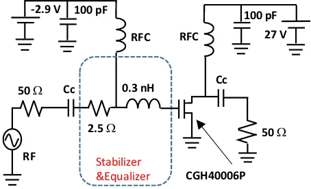
In this study, a general purpose CGH40006P GaN HEMT from Wolfspeed Company is employed as an active device to design a Class-J RF PA over 1.6–2.6 GHz. The bare chip used in this packaged transistor is CGH60008D GaN HEMT device which is used to de-embedding the device parasitic elements. For Class-J operation, as mentioned in the previous section, the optimum gate bias is the transistor pinch-off voltage (Vp) which is−2.9 V for the selected transistor. For reliable operation, it is compulsory to avoid breakdown region. According to the transistor datasheet, the breakdown occurs around 84 V, and therefore, the drain is biased at 27 V which is slightly less than its recommended bias point in the datasheet. The bias sequencer-controller MABC-001000-DP000L from Macom Company is employed to control the dc bias and protect the transistor from low-frequency instability.
Small signal simulation indicates the stability factor below one (K <1), and therefore instability may occur. There are several approaches to improve stability level [13] such as using a resistor in series or parallel with the input or output of the device as recommended in the device’s datasheet. A very high stability factor is also unacceptable because increasing stability factor leads to lower signal gain. On the other hand, gain variation is a common problem in broadband amplifiers due to the gain roll-off. Low gain variation is an important requirement in the modern signal modulations such as OFDM and LTE. Here, a 2.5 Ω resistor in series with a 0.3 nH inductor, as shown in Fig. 3, acts as a stabilizer and gain equalizer for compensating the gain roll-off effect. The simulation results for stability factor (k
factor) and maximum available gain with and without the presence of stabilizer/equalizer circuit are shown in Fig. 4. Since, thekfactor is less than one for the bottom half of the bandwidth, magnitudes of
S(1,1) andS(2,2) are simulated to ensure that they are also less than one, and therefore, the PA works in a stable condition [14]. The resulting S(1,1) and S(2,2) are shown in Fig. 5, which entirely satisfy the stability criteria. This circuit not only improves stability level but also reduces the gain variation and facilitates the design of input matching network by increasing the source impedance value of PA.
-2.9 V
27 V
100 pF 100 pF
RFC RFC
Cc Cc
50 Ω 2.5 Ω
Stabilizer &Equalizer
RF
0.3 nH
CGH40006P 50 Ω
Figure 3. Configuration of stabilizer/equalizer circuit in PA structure.
Figure 4. Small-signal simulation results for stability factor and maximum available gain versus frequency within and without presence of stabilizer/equalizer circuit.
0.2 0.3 0.4 0.5 0.6 0.7 0.8 0.9 1
1.6 1.7 1.8 1.9 2 2.1 2.2 2.3 2.4 2.5 2.6
Mag(S
(1,1
)), M
a
g(S(2,2))
Frequency (GHz)
Mag(S(2,2))
Mag(S(1,1))
Figure 5. Magnitude ofS(1,1) andS(2,2) versus frequency of PA in presence of stabilizer/equalizer circuit, ensuring stability criteria.
Q=2 Q=1
Q=1 Q=2 Zs @ 2.6 MHz
Zs @ 1.6 MHz Series TLs Parallel TLs
Zs= 5
5
j 50 Zs
31° 50
12° 50
11° 50
43° 50
67° 50
78° 50
TL1 TL3
TL5
TL2 TL4
TL6
Ω Ω Ω Ω
Ω Ω Ω
-Ω
(a)
(b)
Figure 6. Conjugated input impedances swept over 1.6–2.6 GHz in steps of 100 MHz with showing input matching network loci at the center frequency and Q curves, (b) configuration of input matching network by 50 Ω microstrip lines.
from the operation of the used stabilizer, the imaginary parts of the input impedances are small enough and bounded within theQ= 2 curve with up to half of the impedances bounded within theQ= 1 curve. Although increasing inductance value will lead to all impedances bounded within the Q = 1 curve, it will also lead to lower bandwidth due to largeQL provided by the inductance. In order to get a facility in the design of the broadband input matching network, a 5−j5 Ω (QL= 1) is adopted for the source impedance. However, selecting this impedance might lead to a slight reduction in power gain at the whole frequency except 2 GHz. The ladder structure of series and parallel 50 Ω transmission lines (TLs) operates as a broadband low-pass filter so that when the TLs values are appropriately determined, an optimum low-loss broadband matching network is realized. This filter is graphically designed based on the method proposed in [15]. The low-pass filter structure for the input (n= 6) matching network using 50 Ω transmission lines is depicted in Fig. 6(b).
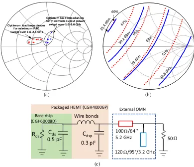
Optimumloadimpedances formaximumoutputpower Optimum load impedances
formaximum PAE
69%
(a) (b)
50
R
ds0.5 pF
100 /64 ° 5.2 GHz Wire bonds
C
dsBare chip (CGH60008D)
External OMN
120 /95°/3.2 GHz
0.3 pF
C
dspPackaged HEMT (CGH40006P)
Ω Ω
Ω
(c) swept over 1.6-2.6 GHz
swept over 1.6-2.6 GHz
Figure 7. Optimum output fundamental load impedances for the maximum PAE and maximum output power swept over 1.6–2.6 GHz in steps of 100 MHz, (b) the second harmonic load pulling contours for the PAE (dashed lines) and the output power (solid lines) as the fundamental harmonic component of load impedance is kept fix at 2.1 GHz, (c) configuration of output matching network.
Keysight’s Advanced Design System (ADS) software is used. The load-pull impedances obtained from simulation for the PAE and output power in steps of 100-MHz at the fundamental and second harmonics are shown in Figs. 7(a) and (b). Fortunately, the optimum impedances are near the center of Smith chart (50 Ω) which facilitates the design of output matching network. A simple low-pass filter structure of microstrip transmission lines proposed here, as shown in Fig. 7(c), appropriately matches the device by the network (50 Ω) at the fundamental harmonic and matches by a low-real value impedance at the second harmonic which is a Class-J requirement. Although the matching network seems as though it is unable to provide definite Class-J load condition, especially for the second harmonics of the early frequencies, it is optimized for output power and PAE parameters by computer-aided simulation as the power amplifier design is completed.
The prototype PA structure is shown in Fig. 8. The designed PA circuit is optimized by ADS for the PAE greater than 60% and the output power greater than 38 dBm (6.3 W) by varying the width and length of all transmission lines. Finally, the electromagnetic (EM) simulation is carried out to predict PA behavior in the real condition.
4. SIMULATION AND EXPERIMENTAL RESULTS
T
-2.9 V27 V
100 pF 100 pF
300 nH 300 nH
20 pF 20 pF 50 0.3 nH 0.5 nH 2.5 Stabilizer &Equalizer 50 42° 2.6 GHz 50 66° 2.6 GHz 50 78° 2.6 GHz 50 31° 2.6 GHz 50 12° 2.6 GHz 50 11° 2.6 GHz 100 /64° 5.2 GHz 120 95° 3.2 GHz RF CGH60008D IMN OMN 0.3 pF 0.3 nH 0.1 pF CGH40006P TL1 TL2 TL 4 TL 6 TL3 TL5 TL7 TL 8 Ω Ω Ω Ω Ω Ω Ω Ω Ω Ω
Figure 8. Prototype schematic of Class-J PA.
10 20 30 40 50 60 70
0 80 0.0
0.5 1.0
-0.5 1.5
Drain voltage (V)
D rai n cur rent ( A
) @ 2.6 GHz
@ 1.6 GHz
Figure 9. Load line of Class-J PA at the intrinsic drain of the bare chip.
-0.5 0 0.5 1 1.5 0 20 40 60 80
0.000 144.7 289.4 434.0 578.7 723.4
Dr ain curr en t ( A ) Dr ain V o ltag e (V ) Time (ns) Vd Id
Figure 10. Time-domain simulation results for drain voltage and current waveforms of prototype Class-J PA at 2.4 GHz.
current lines are appropriately maintained low, around zero. The maximum current rises to near 1.3 A at 2.6 GHz, where the drain voltage is sufficiently small. It also shows that the PA for high-efficiency operation has not been saturated such as Class-F and Class-E PAs and therefore, a proper linearity performance will be expectable. The time-domain simulation results for the drain voltage and current waveforms of the prototype PA at 2.4 GHz are shown in Fig. 10.
The substrate used for fabrication has a 3-mm dielectric thickness, 17-µm copper cladding thickness, and r= 4.2. We used a thick substrate because the lead of packaged transistor CGH40006P is rather wide while the matching network requires small inductance (0.3 nH). The fabricated Class-J PA is shown in Fig. 11. The TL4 is drawn in opposite side with TL2 and TL6 to reduce the coupling effect between the stubs. TL4 and TL8 are also used for the gate and drain DC supply path, respectively. Two 300-nH inductors as RFCs isolate DC signals from RF signals. In order to block DC signals from the input and output ports, two low-ESR capacitors (20-pF) are employed. The PCB dimensions are 42 mm×45 mm. The PCB was screwed on a suitable aluminum heat sink.
Figure 11. Fabricated Class-J PA within its dimensions.
50 55 60 65 70 75 80
10 15 20 25 30 35 40 45
1.6 1.7 1.8 1.9 2 2.1 2.2 2.3 2.4 2.5 2.6
PAE
(%
)
Gain
(d
B)+20,
Pou
t
(dBm
)
Frequency (GHz) Pout
PAE
Gain
Sim. Meas.
Figure 12. Simulation and measurement results for the output power, PAE, and signal gain in steps of 50-MHz.
0 10 20 30 40 50 60 70 80
10 15 20 25 30 35 40 45
0 2 4 6 8 10 12 14 16 18 20 22 24
PAE (
%
)
G
a
in
(d
B), Pout (dBm)
Input power (dBm)
Pout Gain PAE
Linear AM-AM
Figure 13. Measurement results in steps of 1-dB for output power, power gain, and PAE versus input power.
-42 dBc
-2.5 -2 -1.5 -1 -0.5 0 0.5 1 1.5 2 2.5 Frequency offset (MHz)
20
0
-20
-40
-60
-80
-100
Normalized output spectrum (dBc)
Figure 14. The normalized spectrum of output signal versus frequency offset of 2.1 GHz when the PA is driven by a CDMA modulated signal with 1.2288 MHz bandwidth.
1.6 -36
1.7 1.8 1.9 2 2.1 2.2 2.3 2.5 2.6
Frequency (GHz) 2.4 -38
-40
-42
-44
-46
-48
-50
ACLR (dBc)
ACLR1
ACLR2
Figure 15. ACLR1 and ACLR2 at the
1.2288 MHz and 2.4576 MHz respectively versus frequency.
and power gain are sharply reduced in out of band as frequency is increased.
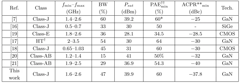
Table 1. Performance comparison of reported PA with different classes.
Ref. Class fmin–fmax (GHz)
BW (%)
Psat (dBm)
PAE††min (%)
ACPR**min
(dBc) Tech. [7] Class-J 1.4–2.6 60 39.2 60* −25 GaN
[16] Class-J 0.5–0.7 33 30 50 - SiGe
[19] Class-E 1.8–2.6 36 28.1 34.5 −28.5 CMOS
[17] HT† 2–3.5 54 30 64 −30 GaN
[18] Class-J 0.65–1.03 45 31 60 −30 CMOS [20] Class-AB 1.2–1.4 15 41 50% −32 GaN [21] Class-AB 1.9–2.5 29 36.9 54.3 −40 GaN This
work Class-J 1.6–2.6 47 39.9 60 −37.8 GaN
* Drain efficiency has been reported.
†Harmonic tuned.
††Minimum PAE across the bandwidth. ** The worst ACLR without linearizer.
To investigate the PA linearity performance, the PA is driven by the CDMA signal with 1.2288 MHz bandwidth at the center frequency of 2.1 GHz. The measured signal is shown in Fig. 14. The adjacent channel leakage ratio (ACLR1) and ACLR2 at 1.2288 MHz and 2.4576 MHz frequency offset are slightly close to−41.9 dBc and −42.1 dBc respectively which indicates proper linearity for this class operation. The signal is symmetrical around center showing less memory effect, and therefore, the PA linearity can be further improved by a linearizer if required. Fig. 15 shows the ACLR1 and ACLR2 over frequency bandwidth in steps of 100 MHz. The worst ACRL1 and ACLR2 occur at 2.4 GHz and are −37.8 dBc and −38.6 dBc, respectively. Overall, they are good results for the linearity performance of the Class-J PA without any linearizer.
5. CONCLUSIONS
In this paper, the design of a broadband, high-efficiency, high linearity Class-J RF PA based on GaN HEMT CGH40006P over 1.6–2.6 GHz is explained in detail. The PA gain variation is controlled using an equalizer. The IMN is obtained from small-signal simulation and designed by a broadband low-pass matching network. The simple OMN is proposed to estimate the Class-J requirements. The designed power amplifier shows the PAE greater than 60% and ACLR1 better than −37.8 dBc throughout the band. The output power is bounded in the range of 39.9–38 dBm across the entire band. Table 1 shows the comparison of the designed power amplifier with other state-of-the-art PA designs, including linear and nonlinear classes. In comparison with [7] and [16], the designed PA shows better linearity performance and power efficiency. This PA shows better linearity than [17, 18] but lower PAEmin while in comparison with [19] and [20], it exhibits better PAEmin and linearity performances over higher fractional bandwidth percentage. This work in comparison with [21] which used Class-AB shows better PAEmin but slightly lower linearity.
ACKNOWLEDGMENT
This work is supported by the National Natural Science Foundation of China (U1603116).
REFERENCES
1. Kazimierczuk, M. K., RF Power Amplifier, John Wiley & Sons, 2014.
power amplifiers with GaN HEMTs,” IEEE Transactions on Microwave Theory and Techniques, Vol. 57, No. 4, 881–889, Apr. 2009.
3. Mohadeskasaei, S. A. and X. Zhou, “A 30 watt high efficient high power RF pulse power amplifier,” IEEE MTT-S International Conference on Numerical Electromagnetic and Multiphysics Modeling
and Optimization (NEMO), 1–3, 2016.
4. Chen, K. and D. Peroulis, “Design of highly efficient broadband Class-E power amplifier using synthesized low-pass matching networks,” IEEE Transactions on Microwave Theory and
Techniques, Vol. 59, No. 12, 3162–3173, Dec. 2011.
5. Chen, K. and D. Peroulis, “Design of broadband highly efficient harmonic-tuned power amplifier using in-band continuous class-F-1/F mode transferring,”IEEE Transactions on Microwave Theory
and Techniques, Vol. 60, No. 12, 4107–4116, Dec. 2012.
6. Cripps, S. C., RF Power Amplifiers for Wireless Communications, Artech House, 1999.
7. Wright, P., J. Lees, J. Benedikt, P. J. Tasker, and S. C. Cripps, “A methodology for realizing high efficiency class-J in a linear and broadband PA,” IEEE Transactions on Microwave Theory and
Techniques, Vol. 57, No. 12, 3196–3204, Dec. 2009.
8. Wu, T., C. Plett, J. W. M. Rogers, and M. Li, “A fully integrated 1–4 GHz GaN class J power amplifier,”IEEE 15th Annual Wireless and Microwave Technology Conference (WAMICON), 1–3, 2014.
9. Alizadeh, A. and A. Medi, “A broadband integrated class-J power amplifier in GaAs pHEMT technology,” IEEE Transactions on Microwave Theory and Techniques, Vol. 64, No. 6, 1822–1830, Jun. 2016.
10. Refai, W. Y. and W. A. Davis, “A highly-efficient, broadband, class-J handset power amplifier using small-size matching network,”IEEE 16th Annual, Wireless and Microwave Technology Conference
(WAMICON), 1–4, 2015.
11. Moon, J., J. Kim, and B. Kim, “Investigation of a class-J power amplifier with a nonlinear Cout for optimized operation,” IEEE Transactions on Microwave Theory and Techniques, Vol. 58, No. 11, 2800–2811, Nov. 2010.
12. Andersson, C. M., M. ¨Ozen, D. Gustafsson, K. Yamanaka, E. Kuwata, H. Otsuka, M. Nakayama, Y. Hirano, I. Angelov, C. Fager, and N. Rorsman, “A packaged 86 W GaN transmitter with SiC varactor-based dynamic load modulation,” European Microwave Conference, 283–286, 2013. 13. Gonzalez, G., Microwave Transistor Amplifiers: Analysis and Design, Vol. 61, Prentice-Hall
Englewood Cliffs, NJ, 1997.
14. Pozar, D. M., Microwave Engineering, John Wiley & Sons, 2011.
15. Grebennikov, A., N. Kumar, and B. S. Yarman, Broadband RF and Microwave Amplifiers, CRC Press, 2015.
16. Wu, R., J. Lopez, Y. Li, and D. Y. C. Lie, “A highly efficient 1-Watt broadband class-J SiGe power amplifier at 700 MHz,”IEEE 12th Topical Meeting on Silicon Monolithic Integrated Circuits in RF
Systems, 69–72, 2012.
17. Xia, J., X. W. Zhu, and L. Zhang, “A linearized 2–3.5 GHz highly efficient harmonic-tuned power amplifier exploiting stepped-impedance filtering matching network,”IEEE Microwave and Wireless
Components Letters, Vol. 24, No. 9, 602–604, Sep. 2014.
18. Park, S., J. L. Woo, U. Kim, and Y. Kwon, “Broadband CMOS stacked RF power amplifier using reconfigurable interstage network for wideband envelope tracking,” IEEE Transactions on
Microwave Theory and Techniques, Vol. 63, No. 4, 1174–1185, Apr. 2015.
19. Son, H. S., W. Y. Kim, J. Y. Jang, I. Y. Oh, and C. S. Park, “A triple-band CMOS class-E power amplifier for WCDMA/LTE applications,” Asia-Pacific Microwave Conference Proceedings
(APMC), 441–443, 2013.
20. Mohadeskasaei, S. A., X. Zhou, S. M. M. Demneh, and S. U. Abdullahi, “A 10 watt class-AB pulse power amplifier,” IEEE MTT-S International Wireless Symposium (IWS), 1–4, 2016.