New De-Embedding Method with Look-Up Table for
Characterization of High Speed Interconnects
Shaowu Huang1, * and Beomtaek Lee2
Abstract—In this paper, a new de-embedding technique with Look-Up Table (LUT) is proposed for accurate and efficient characterization of interconnects, particularly printed circuit board (PCB)
transmission lines including microstrip and stripline. LUT is pre-created to cover various fixture
effects including the reference structures inside and/or outside test printed circuit boards (PCBs). The pre-established LUT is introduced to eliminate the errors of “probing and launching fixtures” in characterization of transmission lines. It is applied to characterization of loss of microstrip and stripline. Simulations and measurements are performed to verify its accuracy and feasibility. Results show it is in good agreement with conventional Delta-L like methods but significantly reduces the cost of characterization. It provides an accurate but cost-effective solution for characterization of high speed interconnects, in particular for high volume manufacturing environments.
1. INTRODUCTION
Characterization of high speed interconnects is important in digital system designs [1–41]. In particular, the accurate and efficient characterization of the transmission lines including microstrips and striplines becomes critical procedure in designing high speed interconnects. The signal distortion and attenuation in transmission lines have been a key issue for printed circuit board (PCB) design and application. The issue escalates as the PCB operates at faster speed and higher frequency. For example, server platforms are designed and under development using many high speed differential I/O buses such as 10G/25G Ethernet, Infiniband EDR (25 Gbps), 8/16 Gbps PCI Express Gen3/4, 24 Gbps SAS 4, etc., and the channel loss have become the bottle neck of these high speed link designs. Therefore, the PCB industry needs accurate and efficient methodologies to qualify and monitor the performance of PCB manufactured by the supply chains. For example, the short pulse propagation (SPP) technique [2], 2x Thru technique such as automatic fixture removal (AFR) method [3], the single-ended TDR/TDT to differential insertion loss (SET2DIL) method [4], the Delta-L method [9], etc. Some of them are recommended by IPC specification [1]. This is extremely important in high volume manufacturing. There are many methodologies which have been developed. There are techniques proposed to reduce the coupon length and improve the accuracy of PCB Tline characterization [5–7], which are critical for high volume manufacturing environment because of the cost concern. Recently the Delta-L method,
which uses vector network analyzer (VNA) to capture the S-parameters then do post-process similar
to SPP, is proposed.
To characterize the transmission line the test structure needs to be built on either test coupon or product PCB. The structure includes probe pad and plated through-hole (PTH) vias. These structures impact a lot on the accuracy of characterization results. There are two types of methods used to de-embed the test fixture effects [1]: one line method, and two line method. One line method refers to a methodology which uses only single test structure, for example, it is one single-ended transmission line in single-ended transmission line characterization, and it is one differential transmission line in
Received 6 November 2015, Accepted 10 January 2016, Scheduled 20 January 2016
* Corresponding author: Shaowu Huang ([email protected]).
differential transmission line characterization. For example, SET2DIL is one line method. Two line method refers to a methodology which uses two test structures, one of them is a “reference” structure used in de-embedding procedure. For instances, SPP, 2x Thru and Delta-L are two line methods. To remove or minimize the effect of these test fixtures, either long line needs to be used in one line method, or two lines need to be built in with different lengths in two line method. However, the disadvantage of the conventional one line method and two line method is that, a large PCB area is needed for long trace and/or reference trace.
In this paper, a new de-embedding technique with Look-Up Table (LUT) is presented for measurements and characterization of high-speed interconnects. A pre-established LUT is introduced to cover various fixture effects including the reference structures inside and/or outside test printed circuit boards (PCBs). It gives several benefits: (1) the LUT provides results of reference structures which can be used to improve the accuracy of de-embedding compared to that of conventional methods with no reference structures; (2) the LUT can be obtained by one time extraction using simulations and/or measurements, which avoids the repeat of building reference structures in the test board and, thus, reduces the cost of measurements and characterization. The presented technique is applied to characterization of transmission lines in printed circuit board (PCB). Both microstrip and stripline are investigated. The effects of vias for stripline characterization are also investigated. Simulations and measurements are performed to test its accuracy. Results show the proposed method has good agreement with the conventional methods with reference structures built in the test board. It reduces the PCB layout area of test structures compared to one line method, and improves the measurement efficiency comparing to two line method. It provides a cost effective but accurate solution for characterization of high speed interconnects.
The paper is organized as follows. In Section 2, we present the methodology for the proposed method. In Section 3, we show the simulation and measurement results for loss characterization of PCB microstrip and stripline. In Section 4, we make conclusions on this work.
2. METHODOLOGY
2.1. Concept of De-Embedding with Look-Up Table (LUT)
Test fixtures include prober (probing and launching fixtures) outside of PCB and test pad/via structures on/inside PCB.
2.2. Effects of Probes outside PCB
Look-Up Table can be pre-established to remove the errors of probing and launching fixtures (prober) outside of PCB
(i) The prober is a separate entity from PCB structure, so it effects can be pre-extracted and tabulated independently from PCB design.
(ii) For given probes, measurements can be used to extract their characterization data asS-parameters.
Note, this is “one time” measurement, the results can be used for any PCB design and tests.
2.3. Effects of Test Pad and vias on or inside PCB
Look-Up Table with theS-parameter files cover the major variations due to PCB layout and stack-up,
for the standardized via structures used in stripline characterization.
(i) LUT can be pre-created for de-embedding the effects of test pad. The structure information (test pad size, anti-pad on reference plane) in horizontal direction can be standardized. The structure information in vertical direction (dielectric thickness to reference plane) can be tabulated. The dielectric material property (dielectric constant and loss tangent) can be tabulated as well.
2.4. Definition of Look-Up Table (LUT)
The information of LUT depends on what type of interconnects to be characterize. For microstrip, the LUT can have three input variables (type of probers, PCB dielectric constant, loss tangent). For stripline, the LUT can have five input variables (type of probers, PCB dielectric constant, loss tangent, length of via through portion, length of via stub portion). Interpolation can be used to generate full LUT from limited pre-extracted data points, which covers full range of variables.
These test fixtures are pre-characterized through either measurement or full-wave electromagnetic field modeling. The pre-characterized information can be built into Look-Up Table (LUT).
(i) The LUT can be updated and extended later on. More variables can be added to take account more variation. The range of a variable can be extended to cover more variation. More accurate measurements and simulations can be used to improve the accuracy.
(ii) The proposed method is a generic technique, which can be combined with many existing methods in [1]. For instance, the developed LUT can be embedded into existing software (4-port VNA, SET2DIL, SPP, Delta-L, etc.). This will significantly reduce the cost and provide desirable solution for high volume manufacturing.
(iii) A generic LUT can be developed for industry product development. Note, in high volume
manufacturing it is desired to recommend/request/standardize the design of probe and test fixtures (test pad, via horizontal dimensions, etc.) for its vendors and customers.
2.5. Application of the Present Method
As described as above, this method can be used for characterization of PCB microstrip and stripline. This method can also be used in characterization of other PCB structures. For instance, this method can be used for characterization of via crosstalk in high speed interconnect. Besides of PCB, this method has great potential applications where the probing and launching can be pre-extracted and tabulated for de-embedding. For instance, characterization of cables, connectors, packages, sockets, On-Chip response, high density interconnect (HDI), etc.
2.6. Transmission Line Characterization with the Present Method
The proposed method can be combined with existing methods such as SPP [2], SET2DIL [4], or Delta-L [8]. It can be used to eliminate the need of reference structure in test board by creating the Delta-LUT. It can also be used to reduce the length of test structure in standard 4-port vector network analyzer (VNA) measurements or time-domain scope measurements such as SET2DIL.Advantages of the present method:
This method has better usage than two conventional methods.
(i) Conventional one line method needs long trace length; >= 8 inches on FR4 PCB and longer than
8 inches on low loss PCB. For example, the differential insertion loss shows errors of 0.18 dB/inch with 4” coupon, 0.09 dB with 8” coupon and 0.05 dB/inch with 16” coupon at 4 GHz where the insertion loss is about 0.72 dB/inch. The error is non-trivial and it requires long length to reduce the error. Of course, the error comes from test fixtures. The novel approach with LUT based de-embedding improves the accuracy with data post-processing and, thus, can reduce the transmission line length. It saves PCB layout area and, thus, the test cost.
(ii) This method is better than conventional two lines method as well. Conventional two line method needs a second line, which takes more board area. This method eliminates the need of second line and, thus, save board area. Also, it can avoid potential issue which can be caused by extra test fixtures of second line.
2.7. Simple Procedure in Pre-extracting the Probing Parasitics from Measurements
• Step 2: use the value in Step 1 to calculate the “new” SDD21 from “old” SDD21 for each coupon.
SDD21 refers to the input differential insertion loss in 4-port mixed-modeS-parameters [42].
Sdd21new= Sdd21original
CouponLength+EquivalentLength
• Step 3: calculate the “difference” (error) of the results of different coupon lengths, and compare the “difference” (error) to the tolerance
– If “difference” (error) <tolerance, go to Step 4
– If “difference” (error)> tolerance, change the equivalent length and go to Step 1, and repeat
the process
• Step 4: calculate Sdd21 for probing parasitic only
Sdd21parasitic =EquivalentLength×Sdd21new
The procedure can be done only once. The probing parasitics can be tabulated. The procedure can be improved through considering the impedance discontinuities and phase.
Note, in this paper we focus on theS21results. However, it can be extended to other cases including
S11 as well.
3. SIMULATIONS
The present method is examined by modeling and simulations using 3D full-wave solver HFSS.
Many cases (microstrip and stripline, varying via stub length) are simulated and the method is applied. All verifies the accuracy of the method. However, in this paper only one case is illustrated due to the page length limit.
3.1. Microstrips
3.1.1. 3D HFSS Models for Microstrip
Figures 1(a)–(c) show the HFSS models used in the simulations to verify the proposed technique. Fig. 1(a) is the microstrip with no test pad. In the simulation, a long microstrip of 12 inches with no test pads is used as benchmark. Fig. 1(b) are the test pads for microstrip probing. Fig. 1(c) is the model for complete test coupon for microstrip with two test pads. In simple implementation, the
S-parameters from Fig. 1(c) are subtracted by two time theS-parameters from test pads in Fig. 1(b).
Through comparing the averaged results (scaled to per inch) to those of Fig. 1(a) with same length, the accuracy of proposed technique can be evaluated.
(a) (b) (c)
3.1.2. Simulation Results
Figures 2(a) and (b) compare the conventional one line method and the proposed technique. Five different lengths are used in the simulations: 1, 2, 4, 8, and 12 inches. It can be seen that, using the new technique, all five different lengths are in good agreement. Single coupon of one inch can give pretty prediction for microstrip. It should be pointed out that the probes outside of PCB are not included in the simulation. In measurements we see better improvement since the probes are included. This further confirms that the effects of fixtures can be pre-extracted and tabulated using look-up table, and new technique enables shorter coupon design and application.
(a) (b)
Figure 2. (a) Original SDD21 for targeted microstrip (dB/inch); (b) New SDD21 for targeted microstrip using proposed de-embedding technique with look-up table. Vertical axis scale: dB/inch.
3.2. Striplines
3.2.1. 3D HFSS Models for Stripline
Figures 3(a)–(c) show the HFSS models used in the simulations to verify the proposed technique. Fig. 3(a) is the stripline with no test pad. In the simulation, a long stripline of 12 inches with no test pads and vias is used as benchmark. Fig. 3(b) is the test pad for stripline probing. Fig. 3(c) is the model
for complete test coupon for stripline with two fixtures. In simple implementation, the S-parameters
from Fig. 3(c) are subtracted by two time the S-parameters from test pads in Fig. 3(b). Through
comparing the averaged results (scaled to per inch) to those of Fig. 3(a) with same length, the accuracy of proposed technique can be evaluated.
(a) (b) (c)
3.2.2. Simulation Results for Stripline
Figures 4(a) and (b) compare the conventional one line method and the proposed technique. Five different lengths are used in the simulations: 1, 2, 4, 8, and 12 inches. It can be seen that, using the new technique, all five different lengths are in good agreement. Single coupon of 2 inches can give pretty prediction for stripline in this case. It should be pointed out that the probes outside of PCB are not included in the simulation. In measurements we see better improvement since the probes are included. This further confirms that the effects of fixtures can be pre-extracted and tabulated using look-up table, and new technique can reduce the coupon length for PCB characterization.
(a) (b)
Figure 4. Comparison of conventional one line method and proposed technique for Stripline with via stub length = 12 mils. (a) Original SDD21 using conventional one line method; (b) New SDD21 using new de-embedding technique with look-up table. Vertical axis scale: dB/inch.
4. MEASUREMENTS
The proposed method is also examined using VNA measurement with test board.
Many cases (microstrip and stripline, varying via stub length) are investigated in experiments, and the proposed technique is applied. All verifies the accuracy of the method. However, in this paper only one case is illustrated to keep the document length short.
4.1. Experiment Setup
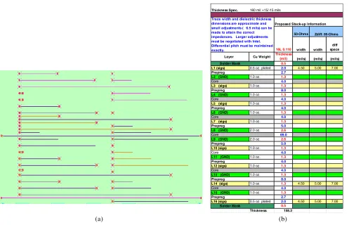
In Figs. 5(a) and 5(b), we show the physical layout and the stack-up of the test board used in the experiment. There are different lengths of test structures for microstrip and stripline. The measurements were performed using 4-port Vector Network Analysis (VNA) with Cable-end electrical calibration. The effects of 450 um GSSG probe and launch effects are included in the original data.
4.2. Measurement Results
4.2.1. Case 1: Microstrip, Layer 1 (Top Layer), No via in PCB Fixture, include External Probe and Launching outside of PCB
(a)
Thickness Spec. 160 mil +15/-15 mils
50-Ohms
16L 0.110 width width diff space Layer Cu Weight Thickness (mil)
(mils) (mils) (mils) Solder Mask 0.5
L1 (sigs) 0.5 oz. plated 2.0 4.50 5.00 7.00
2.7
L2 (GND) 1.0 oz. 1.3
4.0
L3 (sigs) 1.0 oz. 1.3
8.0
L4 (GND) 1.0 oz. 1.3
4.0
L5 (sigs) 1.0 oz. 1.3
4.0
L6 (GND) 1.0 oz. 1.3
4.0
L7 (sigs) 1.0 oz. 1.3
5.0
L8 (GND) 2.0 oz. 2.6
69.0
L9 (GND) 2.0 oz. 2.6
5.0
L10 (sigs) 1.0 oz. 1.3
4.0
L11 (GND) 1.0 oz. 1.3
4.0
L12 (sigs) 1.0 oz. 1.3
4.0
L13 (GND) 1.0 oz. 1.3
8.0
L14 (sigs) 1.0 oz. 1.3 4.50 5.00 7.00
4.0
L15 (GND) 1.0 oz. 1.3
2.7
L16 (sigs) 0.5 oz. plated 2.0 4.50 5.00 7.00
Solder Mask 0.5 Thickness: 158.2 Core Prepreg Prepreg Core Prepreg Core Prepreg Core
Trace width and dielectric thickness dimensions are approximate and small adjustments ( 0.5 mils) can be made to attain the correct impedances. Larger adjustments must be negotiated with Intel. Differential pitch must be maintained exactly.
Proposed Stack-up Information
Zdiff: 85-Ohms Core Prepreg Prepreg Core Prepreg Core Prepreg (b)
Figure 5. The PCB layout and stack-up of the test boards used in the measurements.
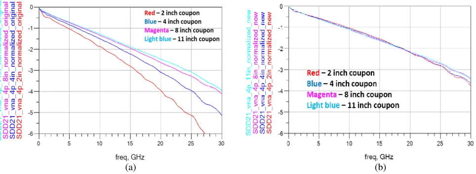
Figure 6. Pre-extracted SDD21 for Case 1 (L1 microstrip) from 4 coupons with different length: 2, 4, 8, and 11 inches. Vertical axis scale: dB.
(a) (b)
Figure 7. Comparison of traditional one line method and new method for Case 1: (a) Original SDD21; (2) New SDD21 using proposed de-embedding technique with look-up table. Vertical axis scale: dB/inch.
Figure 7(b) shows the new SDD21 with de-embedding total probing and launching effects (the probes outside of PCB and the test pad on PCB). It can be clearly seen that, using the proposed method (subtracting out the pre-extracted SDD21 in Fig. 6 from original SDD21 in Fig. 7(a)), the extracted microstrip SDD21 from different coupon lengths are in good agreement. This indicates, this proposed method works for microstrip measurement with one line of 2 inch length. This significantly reduces the board area compared to two line methods and conventional one line methods.
4.2.2. Case 2: Microstrip, Layer 16 (Bottom), with Long via (158 mils) in the Probing Fixture (Probe from Top)
Figure 8 show the SDD21 pre-extracted from 3 different coupons of microstrip on bottom layer with long via (probed from the top) using different routing length: 2, 4, and 8 inches. The pre-extracted SDD21 include total probing and launching effects (the probes outside of PCB and the test pad on PCB). It can be clearly seen that the pre-extracted SDD21 from different coupon lengths are in good agreement. In addition, they have more loss of 0.1 dB at 4 GHz compared to the extracted results from top layer microstrip in Fig. 6. The 0.1 dB is caused by the two long through vias. This further confirms, (1) the probing and launching errors are large (0.9 dB at 4 GHz), (2) the probing fixture effects are separate from PCB coupon design and, thus, (3) one pre-extracted SDD21 can be tabulated and used for all measurements.
Figure 9(a) shows the original SDD21 from 3 different coupons of microstrip on bottom layer with long through via (probed from top) using different routing length: 2, 4, and 8 inches. The original SDD21 are obtained using traditional one line method. There is apparent discrepancy between different coupon lengths in original results. This is due to the probing and launching effects included in the original SDD21. As it is scaled to per inch, shorter coupon gives larger error than longer one.
Figure 8. Pre-extracted SDD21 for Case 3 (L16 microstrip, probed from top, with long via) from 3 coupons with different length: 2, 4, and 8 inches. Vertical axis scale: dB.
(a) (b)
Figure 9. Comparison of traditional one line method and new method for Case 2: (a) Original SDD21; (2) New SDD21 using proposed de-embedding technique with look-up table. Vertical axis scale: dB/inch.
4.2.3. Case 3: Stripline, Internal Layer 14, with Backdrilled via (20 mil via Stub after Back-drilling) in the Probing Fixture
Figure 10 show the SDD21 pre-extracted from 3 different coupons of stripline with via (20 mil stub) using different routing length: 2, 4, and 8 inches. The pre-extracted SDD21 include total probing and launching effects (the probes outside of PCB and the test pad on PCB). It can be clearly seen that the pre-extracted SDD21 from different coupon lengths are in good agreement. They have more loss of 0.1 dB at 4 GHz compared to the extracted results from top layer microstrip in Fig. 6. This further confirms, (1) the probing and launching errors are large (0.8 dB at 4 GHz), (2) the probing fixture effects are separated from PCB coupon design and, thus, (3) one pre-extracted SDD21 can be tabulated and used for all measurements.
Figure 10. Pre-extracted SDD21 for Case 4 (L14 stripline, with via stub length = 20 mils) from 3 coupons with different length: 2, 4, and 8 inches. Vertical axis scale: dB.
(a) (b)
Figure 11. (a) Original SDD21 for targeted transmission line (dB/inch); (b) New SDD21 for targeted transmission line using proposed de-embedding technique with look-up table (dB/inch).
inch, shorter coupon gives larger error than longer one.
Figure 11(b) shows the new SDD21 with de-embedding total probing and launching effects (the probes outside of PCB, and the test pad and vias on PCB). It can be clearly seen that, using the proposed method (subtracting out the pre-extracted SDD21 in Fig. 10 from original SDD21 in Fig. 11(a)), the extracted stripline SDD21 from different coupon lengths are in good agreements. In addition, stripline has 0.45 dB loss at 4 GHz, which agrees with what is expected. This indicates, this proposed method works for measurement of stripline with back drilled via (stub length 20 mils) using one line of 2 inch length. This significantly reduces the board area compared to two line methods and conventional one line methods.
Note that,
(i) The represented fixtures including the cables can have some variations when attached to different PCBs. The impacts of the variations of fixtures can be well controlled if the system assembly and modelled are performed carefully and accurately.
(iii) It is notable that in high volume manufacturing, the cost is a key concern. Although the proposed method may slightly sacrifice a bit accuracy due to the variations of fixtures, the significant reduction in the cost makes it attractive. Cost-effective techniques with good enough accuracy are desirable for high volume production applications. In another word, the proposed method provides a unique valuable solution with good balance between accuracy and cost.
5. CONCLUSION
In this paper, a new de-embedding technique with LUT is proposed for characterization of high speed interconnects. The technique substantially improves the accuracy of the characterization of printed circuited boards (PCBs) through introducing a new de-embedding technique with pre-established LUT. The look-up table can be pre-established through 3D electromagnetic modeling or test fixture measurements. New test fixtures can be characterized with interpolation on existing entries in LUT. In particular, it is suited for characterization of transmission line in PCB. It avoids using second line, which is required in two lines methods. It also reduces the length of test coupon, which is desired in high volume PCB design and applications, particularly for PCB loss measurement. The applications to PCB microstrip and stripline characterizations are investigated using simulations and measurements. Results show the technique is accurate and cost effective for PCB characterizations.
ACKNOWLEDGMENT
The authors thank the engineers and managers of Intel Corporation who contributed to this paper through support, useful discussions and development efforts. The authors would like to thank Jeff Loyer for providing the measurement data and helpful discussions.
REFERENCES
1. IPC-TM-650 Test Methods Manual, (http://www.ipc.org/test-methods.aspx).
2. Deutsch, A., R. S. Krabbenhoft, K. L. Melde, C. W. Surovic, G. A. Katopis, G. V. Kopcsay, Z. Zhou, Z. Chen, Y. H. Kwark, T.-M. Winkel, X. Gu, and T. E. Standaert, “Application of the short-pulse propagation technique for broadband characterization of PCB and other interconnect technologies,”
IEEE Transactions on Electromagnetic Compatibility, Vol. 52, No. 2, 266–287, May 2010. 3. Keysight Application Note, 5990-8443EN, USA, August 1, 2014.
4. Loyer, J. and R. Kunze, “SET2DIL: Method to derive differential insertion loss from single-ended
TDR/TDT measurements,” DesignCon 2010, Santa Clara, CA, USA, 2010.
5. Huang, S., J. Loyer, R. Kunze, and B. Wu, “Method to reduce coupon lengths for transmission
line S-parameter measurements through elimination of guided-wave multiple reflections,” PIERS
Proceedings, 2502–2509, Guangzhou, August 25–28, 2014.
6. Huang, S., J. Loyer, R. Kunze, and B. Wu, “Method to reduce coupon length for S-parameter
measurements,” DesignCon 2015, Santa Clara, CA, January 27–30, 2015.
7. Huang, S., “Method to improve the accuracy of mixed-mode S-parameters derived from
single-ended results and application to shorter test coupon design,” IEEE International Symposium on
Electromagnetic Compatibility, Santa Clara, CA, March 15–20, 2015.
8. Huang, S. and B. Lee, “Novel de-embedding method with look-up table for characterization
of interconnects,” 2015 IEEE 24th Electrical Performance of Electronic Packaging and Systems
(EPEPS), San Jose, CA, October 25–28, 2015.
9. Hsu, J., T. Su, K. Xiao, X. Ye, S. Huang, and Y. L. Li, “Delta-L methodology for efficient PCB
trace loss characterization,” 2014 9th IEEE International In Microsystems, Packaging, Assembly
and Circuits Technology Conference (IMPACT), 113–116, 2014.
10. Ye, X., J. Fan, and J. L. Drewniak, “New de-embedding techniques for PCB transmission-line
11. Kumar, A. and G. Singh, “Measurement of dielectric constant and loss factor of the dielectric
material at microwave frequencies,” Progress In Electromagnetics Research, Vol. 69, 47–54, 2007.
12. Wu, Y. Q., Z. X. Tang, B. Zhang, and Y. H. Xu, “Permeability measurement of magnetic
materials in microwave frequency range using support vector machine regression,” Progress In
Electromagnetics Research, Vol. 70, 247–256, 2007.
13. He, X., Z.-X. Tang, B. Zhang, and Y. Wu, “A new deembedding method in permittivity
measurement of ferroelectric thin film material,” Progress In Electromagnetics Research Letters,
Vol. 3, 1–8, 2008.
14. Tiemeijer, L. F. and R. J. Havens, “A calibrated lumped-element de-embedding technique for
on-wafer RF characterization of high-quality inductors and high-speed transistors,”IEEE Transactions
on Electron Devices, Vol. 50, No. 3, 822–829, March 2003.
15. Cho, M. H., G. W. Huang, K. M. Chen, and A. S. Peng, “A novel cascade-based de-embedding
method for on-wafer microwave characterization and automatic measurement,”2004 IEEE MTT-S
International Microwave Symposium Digest, Vol. 2, 1237–1240, 2004.
16. Chou, Y.-H., M.-J. Jeng, Y.-H. Lee, and Y.-G. Jan, “Measurement of RF PCB dielectric properties
and losses,”Progress In Electromagnetics Research Letters, Vol. 4, 139–148, 2008.
17. Qian, C. and W. B. Dou, “A new approach for measuring permittivity of dielectric materials,”
Journal of Electromagnetic Waves and Applications, Vol. 19, 795–810, 2005.
18. Bogle, A., M. Havrilla, D. Nyquis, L. Kempel, and E. Rothwell, “Electromagnetic material
characterization using a partially filled rectangular waveguide,”Journal of Electromagnetic Waves
and Applications, Vol. 19, No. 10, 1291–1306, 2005.
19. Carroll, J., M. Li, and K. Chang, “New technique to measure transmission line attenuation,”IEEE
Trans. on Microwave Theory and Tech., Vol. 43, No. 1, 219–222, 1995.
20. Zhao, W., H.-B. Qin, and L. Qiang, “A calibration procedure for two-port VNA with three
measurement channels based on T-matrix,”Progress In Electromagnetics Research Letters, Vol. 29,
35–42, 2012.
21. Rumiantsev, A. and N. Ridler, “VNA calibration,” IEEE Microwave Magazine, Vol. 9, No. 3,
86–99, 2008.
22. Ferrero, A., V. Teppati, M. Garelli, and A. Neri, “A novel calibration algorithm for a special class
of multiport vector network analyzers,”IEEE Trans. on Microw. Theory and Tech., Vol. 56, No. 3,
693–699, 2008.
23. Marks, R. B., “A multiline method of network analyzer calibration,” IEEE Trans. on Microw.
Theory and Tech., Vol. 39, No. 7, 1205–1215, 1991.
24. Hasar, U. C., “A fast and accurate amplitude-only transmission-reflection method for complex
permittivity determination of lossy materials,”IEEE Trans. Microw. Theory Tech., Vol. 56, No. 9,
2129–2135, 2008.
25. Hasar, U. C., “A new microwave method based on transmission scattering parameter measurements
for simultaneous broadband and stable permittivity and permeability determination,” Progress In
Electromagnetics Research, Vol. 93, 161–176, 2009.
26. Kaatze, U., “Techniques for measuring the microwave dielectric properties of materials,”Metrologia,
Vol. 47, No. 2, S91–S113, 2010.
27. Zhang, H., S. Y. Tan, and H. S. Tan, “An improved method for microwave nondestructive dielectric
measurement of layered media,”Progress In Electromagnetics Research B, Vol. 10, 145–161, 2008.
28. Le Floch, J. M., F. Houndonougbo, V. Madrangeas, D. Cros, M. Guilloux-Viry, and W. Peng,
“Thin film materials characterization using TE modes,” Journal of Electromagnetic Waves and
Applications, Vol. 23, No. 4, 549–559, 2009.
29. Jin, H., S. R. Dong, and D. M. Wang, “Measurement of dielectric constant of thin film materials
at microwave frequencies,” Journal of Electromagnetic Waves and Applications, Vol. 23, Nos. 5–6,
809–817, 2009.
30. Wu, Y. Q., Z. X. Tang, Y. H. Xu, and B. Zhang, “Measuring complex permeability of
and Applications, Vol. 23, No. 10, 1303–1311, 2009.
31. Challa, R. K., et al., “Permittivity measurement with a non-standard waveguide by using TRL
calibration and fractional linear data fitting,” Progress In Electromagnetics Research B, Vol. 2,
1–13, 2008.
32. Wu, Y., Z. Tang, Y. Yu, and X. He, “A new method to avoid crowding phenomenon in extracting
the permittivity of ferroelectric thin films,”Progress In Electromagnetics Research Letters, Vol. 4,
159–166, 2008.
33. Kharkovsky, S. N., M. F. Akay, U. C. Hasar, and C. D. Atis, “Measurement and monitoring of
microwave reflection and transmission properties of cement-based materials,”IEEE Trans. Instrum.
Meas., Vol. 51, No. 6, 1210–1218, 2002.
34. Nicolson, A. M. and G. Ross, “Measurement of the intrinsic properties of materials by time-domain
techniques,” IEEE Trans. Instrum. Meas., Vol. 19, No. 4, 377–382, 1970.
35. Weir, W. B., “Automatic measurement of complex dielectric constant and permeability at
microwave frequencies,”Proc. IEEE, Vol. 62, No. 1, 33–36, 1974.
36. Smith, D. R. and S. Schultz, “Determination of effective permittivity and permeability of
metamaterials from reflection and transmission coefficients,” Phys. Rev. B, Vol. 65, 195104(5),
2002.
37. Baker-Jarvis, J., E. J. Vanzura, and W. A. Kissick, “Improved technique for determining complex
permittivity with the transmission/reflection method,”IEEE Trans. Microw. Theory Tech., Vol. 38,
No. 8, 1096–1103, 1990.
38. Boughriet, A. H., C. Legrand, and A. Chapoton, “Noniterative stable transmission/reflection
method for low-loss material complex permittivity determination,” IEEE Trans. Microw. Theory
Tech., Vol. 45, No. 1, 52–57, 1997.
39. Mahony, J. D., “Measurements to estimate the relative permittivity and loss tangent of thin,
low-loss materials,” IEEE Antennas Propag. Mag., Vol. 47, No. 3, 83–87, 2005.
40. Muqaibel, A. H. and A. Safaai-Jazi, “A new formulation for characterization of materials based on
measured insertion transfer function,” IEEE Trans. Microw. Theory Tech., Vol. 51, No. 8, 1946–
1951, 2003.
41. Ness, J., “Broad-band permittivity measurements using the semi-automatic network analyzer,”
IEEE Trans. Microw. Theory Tech., Vol. 33, No. 11, 1222–1226, 1985.
42. Bockelman, D. E. and W. R. Eisenstadt, “Combined differential and common-mode scattering
parameters: Theory and simulation,” IEEE Trans. Microw. Theory Tech., Vol. 43, No. 7, 1530–