Abstract—Design, simulation, implementation and measurement results of multiline and multilayer microstrip directional couplers are given with closed form relations. Step-by-step design procedure reflecting the design practice of directional couplers, which requires only information on coupling level, port impedances and operational frequency, is presented. The method based on the synthesis technique applied in the design of conventional two-line microstrip symmetrical directional couplers is adapted to design multilayer directional couplers with the aid of electromagnetic simulators using parametric analysis with curve fitting method. The proposed design method is compared with the measurement results and accuracy is verified. It has been also shown that the directivity of the couplers designed using the multilayer structure is improved significantly. A method such as the one presented in this paper can be used to design multilayer two-line and three-line directional couplers which can be integrated to the front end of an RFID systems to provide the required isolation between transmitter and receiver and prevent signal leakage due to use of conventional circulators.
1. INTRODUCTION
Microstrip directional couplers have been widely used in variety of RF/Microwave applications. The ease of manufacturing and implementation of microstrip type directional couplers make them a good component to detect and transmit desired signals without impacting the performance of the system. The cost effectiveness of the microstrip type directional couplers also make them a viable option for volume manufacturing in the RF industry. The design of conventional microstrip type directional couplers has been well investigated and reported by several researchers [1–5]. The common design method relies on prior knowledge of the physical geometry of the coupler, which requires the use of design charts for the even and odd mode impedances of the structure. The design method that only uses the knowledge of port impedances, coupling level and operation frequency with closed formulation is given in [6, 7]. The three step design procedure and formulation outlined in [6, 7] is also what would be used by designers in practice.
One of the challenges in microstrip type directional couplers is their poor directivity, which usually becomes a problem during sampling of the signals when they are used as power monitoring devices. The poor directivity in essence is due to a discrepancy in phase velocities between the odd and even mode impedances. There have been several compensation methods introduced to improve the directivity of the couplers and enhance the accuracy of the signal sampling. One of the commonly used methods includes using a dielectric overlay on top of the coupled lines [8–11] or implementing wiggling coupled edges of the coupled lines [12–14]. Alternatively, one of the other widely proposed compensation methods includes connecting lumped components at the ends or center of the coupled lines [15, 16]. The discussion of impedance mismatch via additional coupled line and epsilon negative transmission line are presented
Received 22 January 2018, Accepted 21 March 2018, Scheduled 4 April 2018
* Corresponding author: Abdullah Eroglu ([email protected]).
in [17, 18]. It has been shown that high directivity for directional couplers can also be obtained using multilayer configuration [19–21]. The design of the two-line multilayer coupler in [20] is similar to the ones presented in [22, 23] which were conducted with static electric field analysis and full wave analysis based on Green’s functions, respectively. Although there is an extensive literature on the design of multilayer directional couplers [24–26], the design procedure relies on either design charts with the prior knowledge of geometry or numerical analysis. These methods are not practical and hence, there are no closed form relations available yet to design multilayer couplers that would reflect the practice which requires only the knowledge of port impedances, coupling level and operational frequency as outlined in [6, 7]. It is to be noted that the improved directivity, and hence isolation, in microstrip couplers will extend their application and make them a viable alternative to replace the circulators that are widely used in RFID systems and reduce the inherent leakage problem [27, 28].
Conventional microstrip couplers are practical sampling devices and can be used to detect either forward or reverse power in practice because one of the coupled ports is usually terminated with lumped element for compensation to improve the directivity. This problem can be overcome by using three-line microstrip couplers and having one of the ports of the coupled lines as forward signal detection while terminating the other port of the same-coupled line with a lumped element for compensation of the mismatch for directivity improvement. Then, other coupled line can be used for reverse signal detection and same technique can be applied to improve the directivity. The use of three-line microstrip couplers as reflectometers are discussed in [29, 30]. However, the design of three-line microstrip directional couplers in the literature again is based on the use of odd and even mode impedance design charts or numerical analysis techniques as outlined in [31–33].
In this paper, the design, simulation, implementation methods and measurement results for multiline and multilayer microstrip directional couplers with closed form relations are presented. The design procedure for the two-line multilayer coupler shown in Fig. 1 is based on the design method for a two-line conventional microstrip coupler outlined in [6, 7] and requires information for coupling level, port impedances, and operational frequency. The design procedure then requires parametric analysis with the curve fitting method to obtain the closed form relations. The closed form relations are obtained for widely used microwave materials such as TMM10, FR4, RF60, RO4003, and Teflon. The design of a three-line microstrip coupler is accomplished using the design of conventional microstrip two-line coupler by placing the second coupled line on the other side of the main line symmetrically. The analytical method using the techniques presented in [32–34] has been developed to confirm the results obtained in simulation and measurement results for three-line microstrip couplers. The design of multilayer three-line microstrip couplers have then been developed using the technique applied to two-line multilayer microstrip couplers. The analytical results for both two-two-line and three-two-line multilayer microstrip directional couplers have been verified by simulation. Several prototypes have been built and measurements results have been obtained. The agreement between analytical, simulation and experimental results were confirmed. It has been shown that the design techniques presented in this paper can be used to implement high performance multiline and multilayer microstrip directional couplers for several RF and microwave applications including RFID systems and energy harvesting applications.
2. FORMULATION
In this section, the formulation and design steps for a conventional two-line microstrip coupler and for three-line couplers, and then multilayer two-line and three-line couplers have been discussed and detailed.
2.1. Two-Line Microstrip Coupler
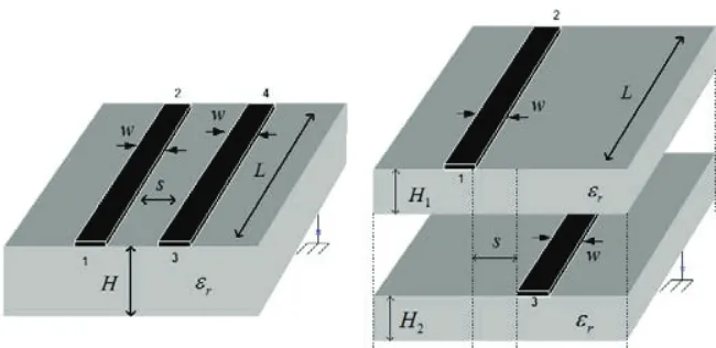
Figure 1. Two-line multilayer microstrip directional coupler with L-length of the coupler,
H2-distance of the coupled line from ground plane,
H=H1+H2-thickness of the dielectric substrate.
Figure 2. Two-line symmetrical microstrip coupler.
microstrip coupler shown in Fig. 2 is based on three steps as outlined in [6, 7]. The first step involves finding the even and odd mode impedances from
Zoe = Z0
1 + 10C/20
1−10C/20 (1)
Zoo = Z0
1−10C/20
1 + 10C/20 (2)
the desired coupling value. In Eqs. (1) and (2), C is the desired coupling value in dB. Then, spacing and shape ratios are found from
s/h= 2
π cosh −1 ⎡ ⎢ ⎢ ⎣ cosh π 2 w h
se + cosh
π 2 w h so −2 cosh π 2 w h so −cosh π 2 w h se ⎤ ⎥ ⎥ ⎦ (3) and w h = 8 exp R
42.4
(εr+ 1)
−1
7 + (4/εr)
11 +
1 + (1/εr) 0.81
exp
R
42.4
√ εr+ 1
−1
(4)
where
R= Zoe
2 or R=
Zoo
2 (5)
(w/h)seand (w/h)so are the shape ratios for the equivalent single case corresponding to even-mode and odd-mode geometry, respectively. (w/h)so is the modified term for the shape ratio. The length of the coupler is the found from
l= λ 4 =
c
4f√εeff
(6)
whereεeff is the effective permittivity constant of the coupled structure and defined as
εeff =
√
εeffe+√εeffo
2
2
εeffe and εeffo are odd and even mode effective permittivity constants. All terms and their related
equations are defined in [7].
2.2. Three-Line Microstrip Coupler
Symmetrical three-line microstrip couplers, which are also known as six port couplers, are shown in Fig. 3 and can be used for several applications including detection of forward and reverse power simultaneously and accurately using phase velocity equalization technique with lumped elements terminated at the ports of the coupling lines.
Figure 3. Three-line symmetrical microstrip coupler.
Figure 4. Generation of three-line coupler from design parameters of two-line coupler.
2.2.1. Step 1: Generate the Design Specifications for a Two-line Coupler Using Equations in Section 2.1
In this step, the required design parameters: coupling level, operational frequency and port impedance, are used to create the design for the two-line symmetrical coupler shown in Fig. 2. Spacing ratio, shape ratio and length of the two-line coupler are then found using Equations (3), (4) and (6).
2.2.2. Step 2: Implementation of Three-Line Couplers
A symmetrical three-line coupler, having the same coupling characteristics of two-line couplers, is then obtained by placing the second coupling line on the other side of the main line by keeping the same spacing with the main line as shown in Fig. 4.
2.2.3. Step 3: Verification of Coupling Levels via Semi-empirical Formulation
The coupling levels of a three-line microstrip coupler are given by the following equations [34]:
K13 = K15=
Zee−Zoo
Zee+Zoo
(8)
K53 =
√
ZeeZoo−Zoe
√
ZeeZoo+Zoe
(9)
whereK13=K15 (not in dB) represents the coupling from the side lines into the main line. K53 is the coupling level between the two-coupled lines.
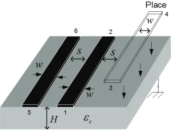
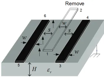
Figure 5. Removal of the main line in three-line coupler for formulation forK13.
found through simulations and integrated to the formulation obtained. After the formulation for K53 is obtained, the relations given in [34] can be used to find three-line mode impedances as
Zoo = Zo
1 +K53 1−K53
1−K13 1 +K13
(10)
Zee = Zo
1 +K53 1−K53
1 +K13 1−K13
(11)
with Zoe =Z0 as shown in [32]. The calculated values using the formulation introduced in this paper are substituted back into Eqs. (8) and (9) to confirm the coupling values between the coupled lines and main line.
K53 given in Eq. (9) depends on the threeline coupler mode impedances Zee,Zoo, and Zoe. Since the coupling level, port impedance and operational frequency are known, then using the formulation in [6, 7], spacing ratio, s/h, and shape ratio, w/h, are obtained. This leads to
dnew = cosh
pi
(w/h) +1
2(s/h)new
(12) where s h new = 2 s h + w h (13)
In Eq. (13),s/h and w/h are the values that are obtained using the formulation in [6, 7]. (w/h)se is the shape ratio for the even modes for the new coupled system and found from
w h se= 2 π cosh −1
(2dnew−g+ 1)
g+ 1
(14)
where
g= cosh
π
2
s
h (15)
The characteristic impedances corresponding to single microstrip shape ratios (w/h)se can be obtained from
Zose = 42.4 log
1 +1 2
64a
(w/h)2se + Δ
1
√ εr+ 1
(16)
Then, the characteristic impedance foroepropagating mode for the coupled lines is equal to
Zoe = 2Zose (17)
In (16), Δ = 64a
(w/h)2se + Δ
2 +
256b
(w/h)2se
where a= 7 11 + 4 11εr
(19a)
and b=
1 0.81
+
1 0.81εr
(19b)
The characteristic impedance of two-line couplers for oomode is then obtained from
Zoo = 1 (2lf Co) −
CeZoe
Co
(20)
whereCe andCo are the capacitances for the even and odd modes, respectively. They are expressed as
Ce = Cp+Cf +Cf (21)
Co = Cp+Cf +Cga+Cgd (22) The relations for the capacitances in Eqs. (21)–(22) are given in [6, 7]. Then,K53for three-line microstrip coupler can then be found from Eqs. (17), (20) with an error function as
K53(dB) = 20 log
Zoe−Zoo
Zoe+Zoo
−erf(εr) (23)
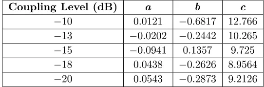
whereerf(εr) =aε2r+bεr+cis defined as the error function and obtained from simulations. The error function is approximated to be a polynomial function of dielectric constant at order 2 and is given in Table 1 below at each coupling level.
Table 1. erf(εr) =aε2r+bεr+c for different coupling levels.
Coupling Level (dB) a b c
−10 0.0121 −0.6817 12.766
−13 −0.0202 −0.2442 10.265
−15 −0.0941 0.1357 9.725
−18 0.0438 −0.2626 8.9564
−20 0.0543 −0.2873 9.2126
2.2.4. Step 4: Calculation of The Mode Impedances for Three-Line Couplers
Equations (10) and (11) can now be used to calculate the mode impedances of three-line couplers to confirm the results.
2.3. Multilayer Microstrip Couplers
There are several benefits in the use of multilayer directional couplers in RF applications including improvement in directivity, better isolation, and providing better performance against arcing for high power applications as outlined before. The design process that will be given in this section can be used to implement both two-line and three-line multilayer couplers in conjunction with the method given in Section 2.2. The illustration of the two-line and three-line multilayer couplers are given in Fig. 6 and Fig. 7. In Fig. 6 and Fig. 7, the dielectric thickness is H and equal to H1+H2.
The step-by-step design procedure to realize two-line and three-line multilayer planar directional couplers are given as follows.
Step 1: Generate Base Design
Figure 6. Illustration two-line multilayer directional coupler.
Figure 7. Illustration of three-line multilayer directional coupler.
Step 2: Simulation for Parametric Analysis
Use simulation to conduct parametric analysis by moving the coupled line at a predetermined distance inside dielectric towards ground plane. Obtain the new coupling for the pre-determined distance and repeat this until the full thickness of the dielectric is reached.
Step 3: Curve Fitting for Equation
Use curve fitting method to obtain equation for the material used for the desired the coupling level to calculate the physical dimensions including the height of the coupled line from the ground plane.
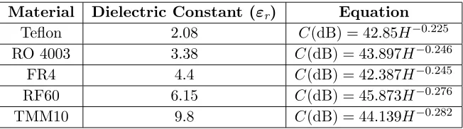
This procedure is applied to commonly used RF materials such as TMM10, FR4, RF60, RO4003 and Teflon where the relative dielectric constant ranges from 2.08 to 9.8 to have the design equations for the two-line multilayer configuration shown in Fig. 6. The three-line multilayer structure shown in Fig. 7 is then formed by application of the procedure described in Section 2.2.
The results for each material are obtained such as the one illustrated in Fig. 8 for Teflon. The summary of the equations, which were obtained using curve-fitting technique for each material, is tabulated in Table 2.
Figure 8. Multilayer coupler parametric analysis results with curve fitting equation for Teflon.
Table 2. Multilayer coupler design equations.
Material Dielectric Constant (εr) Equation
Teflon 2.08 C(dB) = 42.85H−0.225
RO 4003 3.38 C(dB) = 43.897H−0.246
FR4 4.4 C(dB) = 42.387H−0.245
RF60 6.15 C(dB) = 45.873H−0.276
TMM10 9.8 C(dB) = 44.139H−0.282
3. SIMULATION AND MEASUREMENT RESULTS
In this section, simulation and measurement results for several cases of two-line, three-line and multilayer couplers are presented. The base design has been considered as −15 dB coupler at 300 MHz using different substrates.
3.1. Simulation and Measurement Results for Three-Line Microstrip Couplers
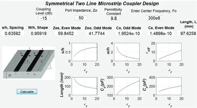
The design of three-line couplers has been implemented by following the steps outlined in Section 2.2. The design process begins with the creation of two-line couplers at 300 MHz for −15 dB coupling level. The substrate material is chosen to be TMM10, which has relative dielectric constant of 9.8. Matlab GUI shown in Fig. 9 is used to generate the physical dimensions to simulate a two-line coupler. Several other parameters, including spacing and shape ratios versus relative dielectric constant, odd and even mode capacitance variation, length, etc., are calculated and illustrated in this GUI.
Once all the physical dimensions are obtained, simulation can be performed. The simulation is done by choosing the thickness of the material to be 100 mils due to availability of material thickness in practice. This gives the calculated spacing to be 63 mils and width to be 95.9 mils. The tolerance of the milling machine allows having 65 mils and 100 mils spacing and width instead of the calculated values. This small deviation is expected to produce minimal error. The layout of the simulated of two-line microstrip coupler with Ansys Designer is illustrated in Fig. 10.
The simulation results for the two-line coupler illustrated in Fig. 10 are shown in Fig. 11. The results show that the coupling level is−17.266 dB and the isolation level is −27.458 dB.
Figure 9. Two-line microstrip coupler design for 15 dB coupling using Alumina as a substrate.
Table 3. Three-line microstrip coupler design parameters for TMM10.
Coupling Level (dB) F (MHz) Material εr s/h w/h
−15 300 TMM10 9.8 0.63592 0.95919
K12(dB) K13(dB) Zoe (Ω) Zoo (Ω) Zee (Ω) L (mils)
−15 −33.3976 50 43.6002 62.4608 3843.5433
Figure 10. Two-line microstrip coupler with 2D view.
Figure 11. Simulation results of two-line microstrip coupler at 300 MHz for Coupling Level = S13 =
−17.266 dB and Isolation Level =S14=−27.458 dB.
The simulation results showing coupling and isolation levels at 300 MHz are given in Fig. 13. The simulation results give almost identical coupling and isolation levels as −17.31 dB and−27.52 dB, respectively.
Figure 12. 3 line microstrip coupler with 2D view.
Figure 13. Simulation results of three-line microstrip coupler at 300 MHz for Coupling Level = −17.31 dB and Isolation Level =−27.52 dB.
Figure 14. The prototype of three-line directional coupler using TMM10 material.
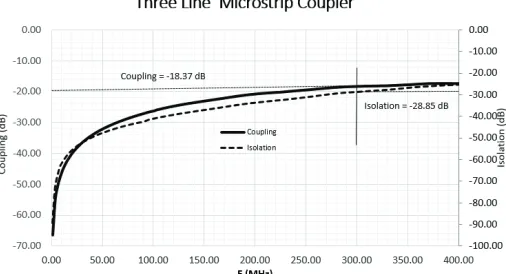
Figure 15. Measurement results for three-line coupler at 300 MHz for Coupling Level = −18.37 dB and Isolation Level =−28.85 dB.
is 100 mils and the spacing of the coupled line from the main line is 65 mils. The substrate used in the prototype is Rogers TMM10 material as illustrated in Fig. 14. The measurement results for coupling and isolation are shown in Fig. 15. Measurement has been done using E5063A Keysight Network Analyzer. The coupling and isolation levels are measured at 300MHz and shown in Fig. 15.
The measured values of coupling and isolation levels are found to be −18.37 dB and −28.85 dB, respectively. These are close to the analytical and simulated values.
3.2. Simulation and Measurement Results for Multilayer Microstrip Couplers
In this section, two-line and three-line multilayer directional coupler designs will be presented. The base design is considered to produce−15 dB coupling using FR4 material as a substrate. Two-line and three-line multilayer coupler configurations were designed and simulated. Several prototypes have been built and measured.
Level (dB) F (MHz) Material Constant (εr) s/h w/h L (mils)
−15 300 FR4 4.4 0.43435 1.8621 5255.24
Table 5. Calculated physical dimensions for multilayer two-line coupler design.
Coupling Level (dB) F (MHz) Material εr Port Imp (Ω) −15 300 FR4 4.4 50 s (mils) w (mils) L (mils) H2 (mils) H (mils)
13.1331 193.4027 5071.3009 55.8175 120
Figure 16. Simulation results of two-line microstrip coupler at 300 MHz for Coupling Level =−15.54 dB and Isolation Level =−22.50 dB.
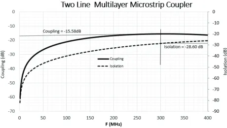
Figure 17. Simulation results of two-line multilayer microstrip coupler at 300 MHz for Coupling Level = −15.58 dB and Isolation Level =−28.60 dB.
The design method in Section 2.3 is now applied to obtain the three-line multilayer coupler as illustrated in Fig. 7. The coupler is simulated using the physical dimensions obtained. The coupling and isolation levels are obtained to be −15.79 dB and −28.76 dB as shown in Fig. 18, respectively. All directional coupler configurations were built and measured. The prototypes that were built are shown in Fig. 19.
The prototypes have been measured and results are tabulated in Table 6. It has been shown that the analytical, simulation, and measurement results are all in agreement.
Figure 18. Simulation results of two-line multilayer microstrip coupler at 300 MHz for Coupling Level =−15.79 dB and Isolation Level =−28.76 dB.
(a)
(b)
(c)
(d)
Figure 19. The prototype of microstrip couplers using FR 4 material for−15 dB coupling. (a) Two-line coupler design. (b) Three-line coupler design. (c) Two-line multilayer coupler design. (d) Three-line multilayer coupler design.
Table 6. Measurement Results for two-line and three-line multilayer couplers.
Coupler Type Frequency (MHz) Coupling (dB) Isolation (dB)
Two Line 300 −13.91 −22.45
Two Line Multilayer 300 −13.72 −26.29
Three Line 300 −13.85 −21.94
Several prototypes have been built and tested after verification of the results between analytical and simulation values. Based on the analytical, simulation and measurement results, the design method proved to be an accurate method within acceptable error to implement any type of two- and three-line multilayer structures. It has also been shown that the implementation of multilayer structure improves the directivity level around 4 dB to 6 dB based on the simulation and measurement results. This is due to improved equalization of the odd and even mode velocity due to implementation of multilayer configuration. The proposed method can also be extended to include inhomogeneous structures where each layer can be a different material. This can be done following the parametric analysis with curve fitting method outlined in Section 2.2 and 2.3. The practical method and results presented in this paper can be used for several RF and microwave applications including RFID systems and energy harvesting applications.
REFERENCES
1. Bryant, T. G. and J. A. Weiss, “Parameters of microstrip transmission lines and coupled pairs of microstrip lines,”IEEE Trans. Microwave Theory Tech., Vol. 16, No. 12, 1021–1027, Dec. 1968. 2. Kirschning, M. and R. H. Jansen, “Accurate wide-range design equations for frequency-dependent
characteristic of parallel coupled microstrip lines,”IEEE Trans. Microwave Theory Tech., Vol. 32, No. 1, 83–90, Jan. 1984.
3. Akhtarzad, S., T. R. Rowbotham, and P. B. Jones, “The design of coupled microstrip lines,”IEEE Trans. Microwave Theory Tech., Vol. 23, No. 7, 486–492, Jun. 1975.
4. Hinton, J. J., “On design of coupled microstrip lines,” IEEE Trans. Microwave Theory Tech., Vol. 28, No. 3, 272, Jul. 1980.
5. Gupta, K. C., R. Garg, and R. Chadha,Computer-aided Design of Microwave Circuits, Chapter 3, Artech House, Massachusetts, 1981.
6. Eroglu, A. and J. K. Lee, “The complete design of microstrip directional couplers using the synthesis technique,”IEEE Trans. Inst. Meas., Vol. 57, No. 12, 2756–2761, 2008.
7. Eroglu, A., RF Circuit Design Techniques for MF-UHF Applications, 1st Edition, CRC Press, Florida, 2013.
8. Sheleg, B. and B. E. Spielman, “Broadband directional couplers using microstrip with dielectric overlays,” IEEE Trans. Microwave Theory Tech., Vol. 22, 1216–1220, Dec. 1974.
9. Paolino, D. D., “h4IC overlay coupler design using spectral domain techniques,” IEEE Trans. Microwave Theory Tech., Vol. 26, 646–649, Sept. 1978.
10. Klein, J. L. and K. Chang, “Optimum dielectric overlay thickness for equal even- and odd-mode phase velocities in coupled microstrip circuits,” Electronics Letters, Vol. 26, 274276, 1990.
11. Su, L., T. Itoh, and J. Rivera, “Design of an overlay directional coupler by a M-wave analysis,” IEEE Trans. Microwave Theory Tech., Vol. 31, 1017–1022, Dec. 1983.
12. Podell, A., “A high-directivity microstrip coupler technique,” 1970 IEEE MTT-S Int. Microwave Symp. Dig., 33–36, 1970.
14. Uysal, S., Nonuniform Line Microstrip Directional Couplers and Filters, Artech House, Norwood, 1993.
15. Phromloungsri, R., M. Chongcheawchamnan, and I. Robertson, “Inductively compensated parallel coupled microstrip lines and their applications,” IEEE Trans. Microwave Theory Tech., Vol. 54, No. 9, 3571–3582, Nov. 2006.
16. Lee, S. and Y. Lee, “A design method for microstrip directional couplers loaded with shunt inductors for directivity enhancement,” IEEE Trans. Microwave Theory Tech., Vol. 58, No. 4, 994–1002, Apr. 2010.
17. Yoshioka, H., A. Hirota, H. Ishibashi, N. Yoneda1, and M. Miyazaki, “A directivity enhancement for directional couplers using additional coupled lines,”IEICE Electronics Express, Vol. 13, No. 18, 20160317, 2016.
18. Pourzadi, A., A. R. Attari, and M. S. Majedi, “A directivity-enhanced directional coupler using epsilon negative transmission line,” IEEE Trans. Microwave Theory Tech., Vol. 60, No. 11, 3395– 3402, Apr. 2012.
19. Horno, M. and F. Medina, “Multilayer planar structures for high directivity directional coupler design,” IEEE Trans. Microwave Theory Tech., Vol. 34, No. 12, 1142–1449, Dec. 1986.
20. Jaisson, D., “Multilayer microstrip directional coupler with discrete coupling,” IEEE Trans. Microwave Theory Tech., Vol. 48, No. 9, 1591–1595, Sept. 2000.
21. Eroglu, A., R. Goulding, P. Ryan, J. Caughman, and D. Rasmussen, “Novel broadband multilayer microstrip directional couplers,” 2010 IEEE AP-S, Dig., 1–4, Jul. 2010.
22. Papatheodorou, S., R. F. Harrington, and J. R. Mautz, “The equivalent circuit of microstrip cross over in a dielectric substrate,”IEEE Trans. Microwave Theory Tech., Vol. 38, 135–140, Feb. 1990. 23. Papatheodorou, S., R. F. Harrington, and J. R. Mautz, “Full wave analysis of microstrip cross
over,” IEEE Trans. Microwave Theory Tech., Vol. 38, 1439–1448, Oct. 1990.
24. Nedil, M., T. A. Denidni, and L. Talbi, “CPW multilayer slot-coupled directional coupler,” Electronics Letters, Vol. 41, No. 12, 706–707, Jun. 2005.
25. Abdelghani, L. M., T. A. Denidni, and D. M. Nedil, “Ultra-broadband 4×4 compact Butler matrix using multilayer directional couplers and phase shifters,”2012 IEEE/MTT-S International Microwave Symposium Digest, 1–3, 2012.
26. Grys, D.-B., R. Storch, and T. Musch, “A multisection ultra wideband directional coupler in multilayer broadside coupled stripline technology,” 2016 German Microwave Conference (GeMiC), 39–42, 2016.
27. Park, K. H., T. Y. Kang, Y. H. Choi, et al., “900 MHz passive RFID reader transceiver IC,” Proceedings of the 36th European Microwave Conference, 1675–1678, Manchester, UK, Sept. 2006. 28. Gagnon, A. and A. Eroglu, “Multilayer coupler design and implementation for RFID systems and
energy harvesting applications,”2016 IEEE/ACES Digest, 1–2, May 2016.
29. El-Deeb, N. A., “The calibration and performance of a microstrip six-port rdlectometer,” IEEE Trans. Microwave Theory Tech., Vol. 31, No. 7, 509–514, 1983.
30. Eroglu, A., Introduction to RF Power Amplifier Design and Simulation, 1st Edition, CRC Press, Florida, 2015.
31. Abdallah, E. and N. El-Deeb, “On the analysis and design of three coupled microstrip lines,”IEEE Trans. Microwave Theory Tech., Vol. 33, No. 11, 1217–1222, Nov. 1985.
32. Pavlidis, D. and H. L. Hartnagel, “The design and performance of three line microstrip directional couplers,”IEEE Trans. Microwave Theory Tech., Vol. 24, No. 10, 631–640, Oct. 1976.
33. Tripathi, V. K., “On the analysis of symmetrical three line microstrip circuits,” IEEE Trans. Microwave Theory Tech., Vol. 25, No. 9, 726–729, Sept. 1977.