85 |
P a g e
DESIGN OF COMBINATIONAL S-BOX
IMPLEMENTED AES ALGORITHM FOR MULTIPLE
FAULT DETECTION SCHEME
V.Nanuku Naik
1, P. Michael Cholines
2 1Pursuing M.tech (VLSI),
2Assoc.Professor (ECE),
Nalanda Institute of Engineering and Technology (NIET), Siddharth Nagar, Kantepudi (V),
Sattenpalli (M), Guntur Dist, A.P. (India)
ABSTRACT
In this paper we are designing combinational S-box based AES. The Advance encryption is method of
encrypting the data with n varied sizes. AES will have sub byte transformation as one of the step that will be
performing to make encryption. The proposed method will have combinational logic based Substitution box,
where in existing system will have S-box as a look up table such that it needs a memory. The sequential circuits
are slower than the combinational designs. Since instead of the ROM based look up table we will implement it
as a combinational design such that its having less complexity and high speed. All of the modules in the
architecture are designed using Verilog HDL, it is synthesized in Xilinx ISE 13.2i.
Keywords: S Box, Sub Byte, Shift Rows, Mix Columns, Add Round Key.
I.
INTRODUCTION
Encryption is a process of converting data from readable format to unreadable format. The readable format
called as plain text. The unreadable data format we called as cipher text. The process used to convert the
algorithm we call as cipher. There are especially two types of algorithms are existing are Data encryption
standard and Advance encryption standard. Any encryption algorithm will comprise of data as one input,
another parameter that is required to convert the data we call as key so we say that second input is key. The DES
will have data size of 64 bit and key size of 56 bit. This is inefficient due to smaller size of data and key. It also
has one more drawback of asymmetric key. In the year 1991 the NIST called up for the new encryption
algorithms. They have conducted several examinations on the received encryption methods; among them they
have selected 5 algorithms are RC6, Rjindael, Mars, Serpent and Two fish. They have subjected those
algorithms to further rounds and they found Rjindael algorithm is the best algorithm. The scientist named
Rjindael proposed an algorithm which is efficient than the DES. The AES will have data size and key size are
variable i.e data size may be 128,196,256 etc, the key size may also varies with 128 , 194 and 256 bit. It is
having certain stages all are performed in loop passion called as round. The algorithm will performed in certain
86 |
P a g e
10,12 and 14 rounds based on key size of 128,194,256 respectively. In each round it will perform four stages
that might be sub byte transformation, shift rows , mix columns and add round key.
The advance encryption standard key size will affects the number of rounds that it will perform on the given
data. The encryption will secure the data by making conversion to the unknown format. It is more secure due to
its complex process. The software design of AES will be easy and less secure, that needs slowest process, to
support high data rate, high bit width communications we need to implement it in hardware. The existed AES
using look up table in the sub byte trans formation, but in proposed method we are using combinational circuit
based s-box make the system highly secure, speed and fault detectable.
I
I. AES ALGORITHM
The AES is advance encryption standard which was proposed by the scientist Rjindael. The encryption is the
process of transforming data from known format to unknown format. That encrypted data can be understood
only by the person who possesses special skill on cryptography. The Advance encryption standard will have
input as data and key. It accepts data and key as block of 32 bits with minimum size of 128 bit and maximum
size of 256bit. The AEs is more complex process such that it will perform certain loops. The AES is generally
performed as set of four stages. The four stage cumulatively called as round. The number of rounds that are
performing will be varied based on the key size used in the AES. The rounds may be 10,12,14 with
corresponding key sizes are 128,196 and 256bits. The four stages are namely sub byte transformation, shift
rows, mix columns and add round key. The final round will accomplish with only three stages remaining all
rounds will contain all stages of AES. Each round will use distinct key in the AES. All several keys are
generated by using Key expansion algorithm. The key expansion algorithm will supply all keys that are needed
to add round key.In this paper we are concentration on 128 bit data and 128 key sizes. The data will be given to
the first stage i.e sub byte transformation then transformed data will be given to the shift rows, then the shifted
data will be giving to the mix column and finally the output data from mix columns will be given to the final
round add round key where data and key will added. The 128 bit data is divided into 16 blocks each consist of
one byte of data. The data 16 blocks are called as states. The 16 states are arranged in 4*4 matrixes. Complex
mathematical operation will be performed on the data at each stage of the AES. The all operations areGalois’s
87 |
P a g e
.
Fig:1 Existing flow chart for AES algorithm
2.1 Sub Byte Transformation
This is the first and foremost step in the AES. In this step each byte in the input data will be replaced with pre
calculated data from the pre calculated table this will be continued until completion of all states. That table we
call as S-box which contains all values from 0 to 256 and its associated values of calculation. This S-box is
implemented as Look up table Rom which makes delay of the circuit. It is the nonlinear step, i.e each byte is
individually replaced irrespective of the other byte
88 |
P a g e
2.2 Proposed Design of Aes
Fig: 3proposed design flow chart
The proposed advanced encryption standard wills also having the same stages as presented in the existing
system except to the small change in the sub byte transformation stage. This is also using in key expansion
algorithm. In sub byte transformation we have pre calculated table which actually implemented as ROM Look
up table in existing designs. The look up table will have unbreakable delay, it will not support pipe lining andits
having the possibility that hackers may hack the S-box such that we can identify errors in it.
To avoid all these problems we are implementing hardware level S-box design using combinational structure.
To make transformation we actually perform multiplicative inversion and affine transformation to get the
resultant values. Now we have to realize them on the input data. Data input for the S-box is eight bit output is
also eight bit i.e one byte. The hardware realization of S-box is shown in block diagramWe have implemented
combinational S-box as five important blocks.Amongthem first three blocks performs multiplicative inversion.
The last two blocks will perform affine transformation.it also includes parity mechanism to avoid faults in the
design. It will perform transformation on single byte atatime such that input will be 8bit. The Eight bit input will
be given to the first block called isomorphic transformation which converts data from binary to Galois field such
that all calculation can be performed very easily. Then they will be divided into four bits and fed to the exoring
block and squaring block. The squaring block which perform squaring of the taken data.Then it will multiply
with constant lambda. Lower bits of the data will be Xored with upper bits and then the result will be added to
the product at the lambda.
89 |
P a g e
β---isomorphic transformation
X--- Multiplication
Xλ---multiplication with lambda
x2---Squarer
δ- 1
---inverse isomorphic transformation
X-1--- Multiplicative inversion
Where q is 8 bit incoming data
β ×q =
×
β -1 ×q =
×
Fig: 5 Isomorphic transformations,Fig: 6Inv isomorphic transformations
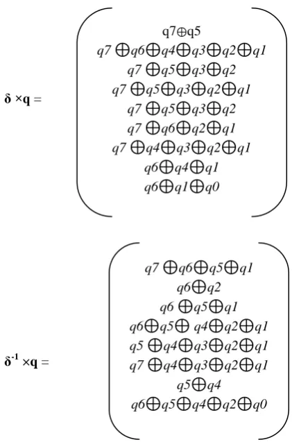
2.3 Isomorphic Transformation
To perform multiplicative inversion first we have to spilt the data from higher order bits to lower order bits such
as GF(28) into GF(21),GF(22)…etc. To accomplish multiplicative inversion we also need conversion from
composite field to Galois field such that it will be very easy to perform operation in Galois field. The
isomorphic transformation ispresented in matrix form as shown in below. That was denoted by δ is an 8*8
matrixes and multiplication is AND operation, addition is modulo-2 addition.
Where q is 8 bit incoming data
1 0 1 0 0 0 0 0
1 1 0 1 1 1 1 0
1 0 1 0 1 1 0 0
1 0 1 0 1 1 1 0
1 1 0 0 0 1 1 0
1 0 0 1 1 1 1 0
0 1 0 1 0 0 1 0
0 1 0 0 0 0 1 1
1 1 1 0 0 0 1 0
0 1 0 0 0 1 0 0
0 1 1 0 0 0 1 0
0 1 1 1 0 1 1 0
0 0 1 1 1 1 1 0
1 0 0 1 1 1 1 0
0 0 1 1 0 0 0 0
0 1 1 1 0 1 0 1
90 |
P a g e
δ ×q =δ-1 ×q =
Fig 7. Isomorphic and inv isomorphic equations
2.4 Affine Transformation
The affine transformation which will performed after multiplicative inversion to accomplish the sub byte
transformation, the sub byte transformation output will same as the pre calculated value after affine
transformation. AT stands for affine transformation, the incoming data is denoted by “a”.
AT(a) = × ⊕
a7
a6
a5
a4
a3
a2
a1
a0
1 1 1 1 1 0 0 0
0 1 1 1 1 1 0 0
0 0 1 1 1 1 1 0
0 0 0 1 1 1 1 1
1 0 0 0 1 1 1 1
1 1 0 0 0 1 1 1
1 1 1 0 0 0 1 1
1 1 1 1 0 0 0 1
0
1
1
0
0
0
1
1
q7⊕q5q7
⊕
q6⊕
q4⊕
q3⊕
q2⊕
q1q7
⊕
q5⊕
q3⊕
q2q7
⊕
q5⊕
q3⊕
q2⊕
q1q7
⊕
q5⊕
q3⊕
q2q7
⊕
q6⊕
q2⊕
q1q7
⊕
q4⊕
q3⊕
q2⊕
q1q6
⊕
q4⊕
q1q6
⊕
q1⊕
q0q7
⊕
q6⊕
q5⊕
q1q6
⊕
q2q6
⊕
q5⊕
q1q6
⊕
q5⊕
q4⊕
q2⊕
q1q5
⊕
q4⊕
q3⊕
q2⊕
q1q7
⊕
q4⊕
q3⊕
q2⊕
q1q5
⊕
q491 |
P a g e
AT-1(a) = × ⊕Fig: 8Affine transformations.
2.5 Shift rows
In this step the input will be taken from the sub byte. The data which is arranged in the states, the rows of the
states are shifted cyclically to little number of bits to the left. The first row of states will be not be changed. The
second has to of states has to be shifted by one bit, third and fourth rows will be shifted accordingly three two
and three bits. Inverse shift rows will accomplish with rows are cyclically shifted few number of bits to the
right. The first row is an unaltered. The second row will be shifted by one bit successively all rows will be
shifted by two and three bits.
Fig; 9 Shift rows implementation
2.6 Mix Columns
In this stage input is taken from shift rows that will process as output. Each output in the mix column will be
product of column of state matrix with the constant polynomial of Galois field. This design is actually
implemented with module shown in figure below. The module contains combination of X time block followed
by Exoring logic. The Xtime block which consists of combination of Xor logics with logical shift operations.
The whole module works for single state. To accomplish it for all states we have to use four Xtime blocks in the
design.
0 1 0 1 0 0 1 0
0 0 1 0 1 0 0 1
1 0 0 1 0 1 0 0
0 1 0 0 1 0 1 0
0 0 1 0 0 1 0 1
1 0 0 1 0 0 1 0
0 1 0 0 1 0 0 1
1 0 1 0 0 1 0 0
a7
a6
a5
a4
a3
a2
a1
a0
92 |
P a g e
Fig: 10 Mix Column Implementation
2.7 Add Round Key
In this step the Mix column stage output will be fed back as input to it. The key is taken from the key expansion
algorithm which is generated from the initial key of cipher. This adding is done by using Xoring operation
between the individual byte to byte operation of the data and key.
2.8 Key Expansion
In the key expansion algorithm, input key is taken from the cipher key i.e initial key. That will be expanded to
get different keys, this is usually done in several steps are initially it is taking 4 word and produces 44 words. It
will be taking first four words 44 words. The rot word will be produced by making one byte cyclic left shift on
the selected four words. Sub word will be produced by making substitution by te transformation using S-box.
That will be Xored with the constant word, the constant word will have upper three bytes will be zeros. For the
first phase Xoring will be done only to the least significant byte.
IV. SIMULATION RESULTS
In this project we are implementing novel combinational S-box based implementation of AES.The
combinational implementation consists of five different modules which will perform multiplicative inversion
and affine transformation. The Combinational design will yields parallel pipelined implementation with reduced
complexity hardwareand small area occupancy. All of the combinational modules are designed using Verilog
HDL. They are synthesized in Xilinx ISE 13.2i and also simulated in the same. The synthesis and
simulationresults are as follows
93 |
P a g e
Fig: 11 Gate level model for top module
V. SYNTHESIS REPORT
Fig: 12 Area report
94 |
P a g e
5.1 Simulation Result
Fig: 14 Simulation Result
VI. CONCLUSION
In this paper we have analyzed and designed Combinational S-box based AES using Verilog HDL. Individual
and complete modules are synthesized and simulated in Xilinx ISE 13.2i. The proposed design of AES will be
having less reduced complexity with compared to the Existed AES. It also supports parallel pipeline to increase
the throughput of the Encryption process such that proposed idea of s-box will support it. The Proposed design
having high security and fault detection is possible.
REFERENCES
[1] Hoang Trang, Nguyen Van Loi “An efficient FPGA implementation of the AdvancedEncryption
Standard algorithm”
[2] Daemen J., and Rijmen V, "The Design of Rijndael: AES-the AdvancedEncryption Standard",
Springer-Verlag, 2002
[3] FIPS 197, “Advanced Encryption Standard (AES)”, November 26, 2001.
[4] Tessier, R., and Burleson, W., “Reconfigurable computing for digitalsignal processing: a survey”, J.VLSI
95 |
P a g e
[5] Ahmad, N.; Hasan, R.; Jubadi, W.M; “Design of AES S-Box usingcombinational logic optimization”,
IEEE Symposium on IndustrialElectronics& Applications (ISIEA), pp. 696-699, 2010.
[6] Alex Panato, Marcelo Barcelos, Ricardo Reis, “An IP of an AdvancedEncryption Standard for Altera
Devices”, SBCCI 2002, pp. 197-202,Porto Alegre, Brazil, 9 and 14 September 2002.
[7] Mr. Atul M. Borkar, Dr. R. V. Kshirsagar and Mrs. M. V. Vyawahare,“FPGA Implementation of AES
Algorithm”, International Conferenceon Electronics Computer Technology (ICECT), pp. 401-405, 2011
3rd
[8] J. Vijaya and M. Rajaram, "High Speed Pipelined AES with Mix Column Transform," European Journal
of Scientific Research, ISSN 1450-216X Vol.61 No.2 (2011), pp. 255-264.
[9] Priyanka Pimpale, Rohan Rayarikar, Sanket Upadhyay,"Modifications to AES Algoritlun for Complex
Encryption," IJCSNS International Journal of Computer Science and Network Security, Vol.11 No.1 0,
October 2011.
[10] Aluned. H. Sawahneh, "Hardware Design of AES S-box using pipelining structure over GF((24i)".
[11] K.Rahimwmisa, Dr. S. Sureshkumar, and K.Rajeshkumar,"Implementation of AES with New S-Box and
PerformanceAnalysis with the Modified S-Box," International Conference on VLSI, Communication &
Instrumentation (ICVCI) 20J J Proceedings published by International Journal of Computer
Applications® (IJCA).
[12] MooSeop Kim, Juhan Kim, and Yongje Choi, "Low PowerCircuit Architecture of AES Crypto Module
for Wirelesssensor Network," World Academy of Science, Engineering and Technology 8, 2007.
[13] M.Pitchaiah, Philemon Daniel, and Praveen,"Implementation of Advanced Encryption
StandardAlgorithm," International Journal of Scientific &Engineering Research, Volume 3, Issue 3,
March -2012 1ISSN 2229-5518.
[14] Zine EI Abidine, Alaoui Ismaili, and Aluned MOUSSA,"Self-Partial and Dynamic Reconfiguration
Implementationfor AES using FPGA," IJCSI International Journal ofComputer Science, Issues, Vol. 2,
2009 ISSN (Online):1694-0784 ISSN (Print): 1694-081456
AUTHOR DETAILS
V.NANUKU NAIK pursuing is M.tech in VLSI system design from Nalanda institute of
Engineering and technology. He completed his B.tech in Electronics and Communication
Engineering. His research of interest includes VLSI, CMOS Analog, Digital system design
etc.
P. MICHAEL CHOLINES is working as associate professor in Nalanda Institute of
Engineering and technology. He completed his post-graduation in VLSI and his area of