170 | P a g e
DESIGN AND IMPLEMENTION OF LOW
POWER SRAM CELL USING SELF-CONTROLLABLE
VOLTAGE LEVEL
Prerna Chauhan
1, Bal Krishan
2 1Scholar,
2A.P
Electronics Engineering department, YMCAUST, Faridabad
ABSTRACT
Memories are critical parts of most of the digital gadgets and therefore reducing energy intake of memory may be very essential in improving the performance, efficiency and stability. Static Random Access Memory (SRAM) is faster and greater suitable than other such as Dynamic Random Access Memory (DRAM) or Flash Memories. The power performance and speedof SRAM are the most vital difficulty for minimizing the strength all through read and write operations. The primary cause of this paper is to provide anEnergyEfficient Low Power SRAM cell and right here method called “Self Controllable Voltage Logic” are used and numerous processes are mentioned to reap the
higher overall performance. Simulation result of SRAM cellular with decreased strength is carried out using Tanner EDA tool.
Keywords: ISVL,Low Power,LSVL, SRAM, SVl, USVL.
I. INTRODUCTION
Random-Access Memory (RAM) is a type of computer facts storage which stores frequently used application instructions to increase the general speed of a system. A random-access memory device lets in records objects to be read or write in almost the same quantity of time no matter the physical location of statistics in the reminiscence. Each bit in an SRAM is stored on 4 transistors that shape cross coupled inverters. With increased tool variability in nanometers scale technology, SRAM will become an increasing number of vulnerable to noise sources 6T SRAM is a bistable device includes back to back related inverters (M1, M2, M3, and M4) alongsideaccess transistors(M5 and M6) being separately related to 2 complementary bit traces BL and BLb get entry to gadgets which permit to access to inner node of the cell. Two back to back inverters store two states 0 and 1. SRAM cells include a latch and, it's called static memory due to the cell data is saved so long as power is become on and refresh operation isn't required for the SRAM [8]. There are many power reduction techniques such as multi threshold voltage CMOS (MTCMOS) and variable threshold CMOS (VTCMOS) [10]. In the first technique power has been reduced. Effectively by use of high Vt MOSFET switches which disconnects the power supply. If this is applied with memories and flip- flops it
171 | P a g e
in active mode allows full supply voltage and decreased supply voltage appears to be proficient for reducing gate leakage currents [11] as well.
II. 6T SRAM
SRAM cell is made up of six MOSFETs. Each bit in an SRAM is stored on two cross-coupled inverters that formed by four transistors (M1, M2, M3, M4). This storage cell has two stable states which are used to denote 0 and 1. Two additional access transistors serve to control the access to a storage cell during read and write operations [7].
Fig.1: Circuit diagram of 6T SRAM
2.1
SRAM OperationAn SRAM cell has 3 distinct states: standby (the circuit is idle), reading (the data has been requested) or writing (updating the contents). SRAM operating in study mode and write modes must have "readability" and "write stability", respectively. The three exceptional states work as follows:
2.2 Standby
If the word line is not asserted, M5 and M6 the access transistors disconnect the cell from the bit lines. The two
cross-coupled inverters formed by the four transistors M1 – M4 will continue to reinforce each other as long as they
are connected to the supply.
2.3 Reading
In idea, reading handiest requires maintaining the word line WL and reading the SRAM cell state by a single access
transistor and bit line, e.g. M6, BL. Nevertheless, bit lines are relatively long and have large parasitic capacitance.
To speed up reading, a more complicated process is used in practice: The read cycle is started by precharging each
bit lines BL and BLb, i.e., driving the bit lines to a threshold voltage (midrange voltage between logical 1 and 0).
Then asserting the word line WL enables each of the access transistors M5 and M6, which causes the bit line BL
voltage to either slightly decrease (bottom NMOS transistor M3 is ON and top PMOS transistor M4 is off) or
increase (top PMOS transistor M4 is on). It should be noted that if BL voltage increases, the BLb voltage decreases,
172 | P a g e
2.4 Writing
The write cycle begins through applying the value to be written to the bit lines. If we wish to write a 0, we would
apply a 0 to the bit lines, i.e. setting BLb to 1 and BL to 0. This is much like to applying a reset pulse to an SR-latch, which causes the flip flop to change state. A 1 is written by way of inverting the values of the bit lines. WL is then asserted and the value that is to be saved is latched in. This works because the bit line input-drivers are
designed to be much stronger than the relatively weak transistors in the cell itself so they can easily override the
previous state of the cross-coupled inverters. In practice, access NMOS transistors M5 and M6 have to be stronger
than either bottom NMOS (M1, M3) or top PMOS (M2, M4) transistors. This is easily obtained as PMOS transistors
are much weaker than NMOS when same sized. Consequently when one transistor pair (e.g. M3 and M4) is only
slightly overridden by the write process, the opposite transistors pair (M1 and M2) gate voltage is also changed. This
means that the M1 and M2transistors can be easier overridden, and so on. Thus, cross-coupled inverters magnify the
writing process.[7]
III. PROPOSED METHOD
3.1 Self-Controllable Voltage Level (SVL)
SVL is the acronym for Self controllableVoltage Level. SVL technique is used to reduce leakage strength for the duration of standby mode of operation i.e. when clock=0. SVL technique uses a PMOS and a NMOS transistor in parallel as pull up network in addition to pull down network. Pull up transistors gate isconnected with complement of clock signal and pull downtransistors gate terminal is attached with clock .Thisapproach to reduce leakage power makes use of a clock signal asthe manipulate signal to govern supply voltage .As a result the call Self controllable Voltage Level Logic is justified.[1]
173 | P a g e
3.2
Improved Self-Controllable Voltage Level (ISVL)
3.2.1Upper Self-Controllable Voltage Level(USVL)
In Upper Self-Controllable Voltage Level circuit (USVL) the impedance of MOS transistor increases with the width of transistor. PMOS1 having width means it offers high resistance in the path between Vdd and Vd. The
NMOS1 and NMOS2 form a read and write working in normal mode of a cell whereas
NMOS2 act as resistor to reduce current in active mode by connecting upper SVL circuit and reduced leakage
power. [1]
Fig.3: Upper SVL circuit
3.2.2 Lower Self-Controllable Voltage Level (LSVL)
In Lower self-controllable voltage level circuit (LSVL) the impedance of MOS transistor increases with the width of transistor. NMOS1 having width means it offers high resistance in the path between Vddand Vd. The NMOS3
work in SVL mode and PMOS2 and PMOS3 work in normal mode of the cell. PMOS2 act as resistor to reduce
leakage power. The lower SVL circuit not only supply power to active load circuit through the on n-SW and also supplies Vss to the standby load circuit through p-SWs.
174 | P a g e
IV. IMPLEMENTATION & CIRCUIT SIMULATION
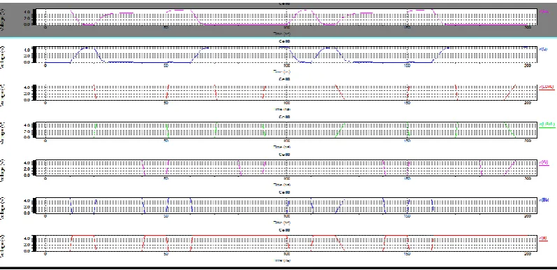
In this paper normal 6T SRAM, 6T SRAM with SVL and 6T SRAM with Improved SVL are simulated on Tanner EDA tool at 180nm technology with different supply voltages and the results are obtained.
3.3SRAM
Fig.5: Circuit of 6T SRAM
175 | P a g e
Table 1: Simulation result of SRAM cell
Power supply(V) Power(w) Delay(s)
0.7 2.083400e-004 1.0640e-008 1.8 3.130410e-004 1.0640e-008 5.0 5.402156e-004 1.0640e-008
3.4SRAM with SVL Technique
Fig.7: Circuit of 6T SRAM using SVL technique
176 | P a g e
Table 2: Simulation result of SVL SRAM cell
Power supply(V) Power(w) Delay(s)
0.7 1.446870e-004 1.1308e-008 1.8 2.496931e-004 1.1671e-008 5.0 2.888867e-004 1.3230e-008
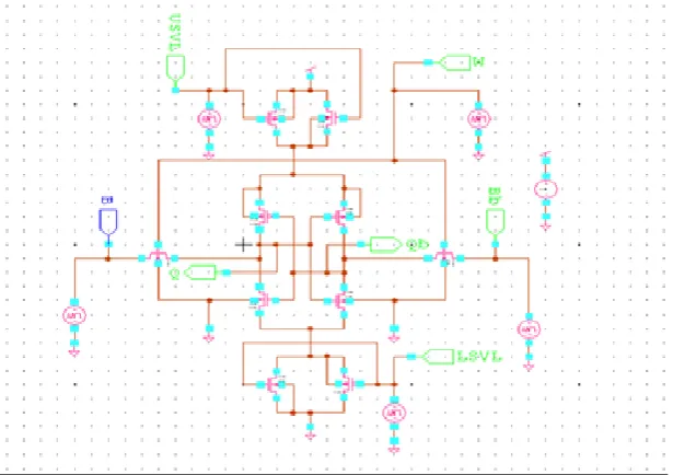
3.5SRAM with ISVL Technique
Fig.9: Circuit of 6T SRAM using ISVL technique
177 | P a g e
Table 3: Simulation result of ISVL SRAM cell
Power supply(V) Power(w) Delay(s)
0.7 1.389026e-004 1.1541e-008 1.8 2.261862e-004 1.1813e-008 5.0 2.808951e-004 1.2908e-008
IV. RESULT
This section deals with the comparison of the entire SRAM cellin terms of Average Power consumed and delay. The results were simulated using TSPICE tanner tool at 180nm technology.
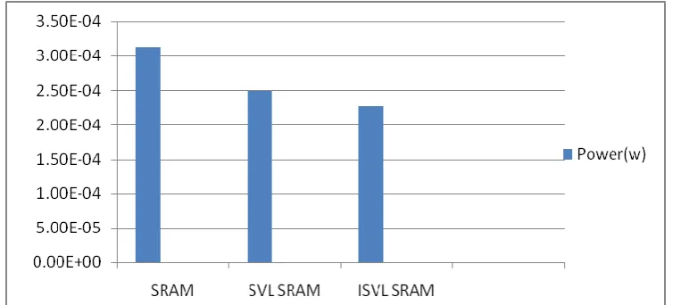
Table 4: Comparison between techniques at 1.8v
Technique Power(w) Delay(s)
SRAM 3.130410e-004 1.0640e-008 SVL SRAM 2.496931e-004 1.1671e-008 ISVL SRAM 2.261862e-004 1.1813e-008
From the above comparison table it is clear that the improved Self-Controllable Voltage Level (ISVL) technique hasminimum averagepower consumption.
Graph 1. Shows the average power consumption
V. CONCLUSION
178 | P a g e
reduction in the power consumption by Improved Self-Controllable Voltage Level (ISVL) with Self-Controllable Voltage Level (SVL) technique is near about 80%. The simulation results are carried out on Tanner EDA tool. 6T SRAM using Improved SVL techniques has better performance than the previous designs.
VI. REFERENCES
1. Amit Grover (2013), “Low Power 7-T SRAM using 90 nm Technology with Tanner Tool”, International
Conference on Artificial Intelligence, Modeling & Simulation.
2. Amit Grover, Neeti Grover, Chetinderpal Singh (2013), “Implementation of a Modified Model-SRAM Using Tanner EDA”, International Conference on Computational Intelligence, Modeling and Simulation.
3. Anand Singh Narwariya, ShyamAkashe (2015), “Minimizing Power Consumption in CMOS Full Subtractor using SVL Technique”, International Journal of Computer Applications (0975 – 8887) Volume 110 – No. 9. 4. AnkitChauhan, D. S. ChauhanandNehaSharan (2016) “Characterization of 6T CMOS SRAM in 90nm
Technology for Various Leakage Reduction Techniques” 2016 IEEE Students „Conference on Electrical, Electronics and Computer Science.
5. B. S. K. Lakshmi, R. Vinay Kumar (2013), “9T SRAM Cell with Improved Self-Controllable Voltage Level Circuits”, International Journal of Technological Exploration and Learning (IJTEL), IJTEL, VOL.2, NO.6.
6. Bhanupriya Bhargava1, Pradeep Kumar Sharma2, ShyamAkashe (2013), “Comparative Analysis of Self- Controllable Voltage Level (SVL) and Power Gating Leakage Reduction Techniques Using in Sequential Logic Circuit at 45 Nanometer Regime”, International Journal of Engineering Research & Technology (IJERT) Vol.
2 Issue 12.
7. Chang-Hoon Choi, Ki-Young Nam, Zhiping Yu, R.W.Dutton (2001), “Impact of Gate Direct Tunneling Current on Circuit Performance: a Simulation Study,” IEEE Transactions on ED, vol. 48, no. 12, pp. 2823-2829.
8. Characterization of 6T CMOS SRAM in 90nm Technology for Various Leakage Reduction Techniques. 9. D. Kumar Gautam, Dr. S.R.P. Sinha and Er. Y. Kumar Verma (2013), “Design a Low Power Half Subtractor
Using AVL Technique Based on 65nm CMOS Technology,” International Journal of Advanced Research in
Computer Engineering and Technology, vol. 2, pp. 2891-2897.
10. Dawoud, DawoudShenouda; R. Peplow (2010) “Digital System Design - Use of Microcontroller” River
Publishers. pp. 255–258.
11. G.Sushma, V. Ramesh (2016), “Low Power High Speed D Flip Flop Design using Improved SVL Technique”,
International Conference on Recent Trends in Information Technology.
12. Garima Jain (2013) “Design and Simulation Low power SRAM circuits”,International Journal for Scientific Research & Development, Vol. 1.
13. Gaurav Dixit, ShyamAkashe (2012), “Leakage reduction in 7T using SVL scheme”, International Conference
on Advanced Computing & Communication Technologies.
179 | P a g e
15. K.N.Yang, H.T.Huang, M.J.Chen, Y.M.Lin, M.C.Yu (2001) “Characterization and Modeling of Edge Direct Tunneling (EDT) Leakage in Ultrathin Gate Oxide MOSFET’s,” IEEE Transactions on ED, vol. 48, no. 6, pp. 1159-1 164
16. K. S. Yeo and K. Roy, Low-Voltage (2005), “Low-Power VLSI Subsystems”. McGraw-Hill.
17. Kaushik Roy, Hamid Mahmoodi-Meimand, and SaibalMukhopadhyay. “Leakage Control for Deep-Submicron Circuits”
18. Kaushik Roy, SaibalMukhopadhyay and Hamid Mahmoodi-Meimand (2003), “Leakage Current Mechanisms and Leakage Reduction Techniques in Deep-Submicrometer CMOS Circuits”, IEEE.
19. Kevin, Z., Embedded Memories for Nano-Scale VLSIs. 2009: Springer Publishing Company, Incorporated.400.