Design of Efficient Air Core Inductors Using a Partial Element
Equivalent Circuit Method
Nikolay Tal1, *, Lisa Shatz2, Yahav Morag1, and Yoash Levron1
Abstract—This paper proposes an optimization method to improve the efficiency of air core inductors, which are frequently employed in near field communication, wireless power transfer, and power conversion systems. We propose a modification to the PEEC based method, which aims at further reducing the computational complexity associated with complex 3D topologies. The main idea is to optimize 3D structures based on a 2D analysis. The device low frequency behavior is estimated based on the full 3D topology, while corrections resulting from high frequency effects are estimated based on a 2D approximation. As a result, since 2D formulations are used to estimate the high frequency effects, it is possible to obtain small mesh sizes, and hence to decrease the computational load, enabling a fast iterative design process. In addition, the proposed method requires no special commercial software, and can be easily implemented in Matlab. Results are compared to a standard commercial FEM tool, CST EM studio, and the results match well.
1. INTRODUCTION
Air core inductors are widely used in number of applications, such as near field communication, inductive power transfer [1–6], lighting impulse tests [7], and power conversion circuits [8–13]. The winding loss in air core inductors may be significantly higher in comparison to magnetic components employing ferromagnetic cores, due to the high number of turns. The copper loss is typically described by the skin and proximity effects, both are due to eddy currents caused by magnetic fields, which become significant at high frequencies. Several research works attempt to accurately estimate these effects [14–37]. In magnetic components that utilize ferromagnetic cores, the conduction losses are typically computed in a two-dimensional (2D) cross section of a winding window using one-dimensional (1D) or 2D models. The 1D solutions of Maxwell equations [14–20] are often based on the Dowell method [14], which assumes that the magnetic field has only one vector component, tangential to the winding layers. The 1D solutions of transformer winding loss are reviewed and summarized in [21]. In 1D methods the following assumptions are made for transformers: (a) the magnetizing current is negligible, and (b) the magnetic field is tangential to the winding layers. While these assumptions are valid for number of transformers, they lead to poor accuracy in cases when the 2D effects cannot be neglected [22–26].
These 2D effects are evaluated using several numerical methods, such as the Finite Element Method (FEM) [38], which is employed in commercial software tools (e.g., Maxwell by Ansys [39], and CST EM studio [40]). However, this approach requires heavy computational resources, which lead to long simulation times, and hence, optimizing the geometry for the least resistance is a time consuming task. For example, a simulation using a genetic algorithm reported calculation times of 20 hours for a simplified FEM model [27]. Addressing these problems, a number of semi-numerical methods are proposed in [28–30]. With these, the parameters of the closed form formula are derived from a
Received 27 July 2017, Accepted 18 October 2017, Scheduled 5 November 2017 * Corresponding author: Nikolay Tal ([email protected]).
set of previously performed numerical simulations. However, these approaches are limited to a single case study, and may still require significant computational resources.The above works were aimed for transformer design, assuming zero total current in the winding window cross section, and negligible magnetization current. Similar methods have also been considered for calculating the ac resistance of inductors [31]. A review and comparison of these methods is provided in [32]. Furthermore, an analytic solution for inductors employed in power silicon integrated circuits (IC) is proposed in [33].
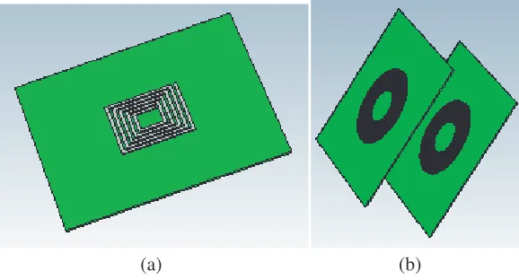
Air core inductors are usually designed by means of numerical methods. An air core inductor and an air core transformer used for inductive power transfer are illustrated in Figs. 1(a) and (b), respectively. The most accurate method for estimating the winding losses is a direct numeric simulation, for example by using the FEM method [38], which is based on the differential form of the Maxell’s equations. The FEM is a general purpose method that may handle various materials, such as conductors, dielectrics, and magnetic materials. In this method, the entire space, including the background computation box, is meshed using triangles in 2D or tethrahedra in 3D. This results in a large yet sparse system of equations, which is solved under the constraints imposed by boundary conditions [41, 42]. The downsides of the FEM method are mainly (a) many elements, since the entire space is meshed, and (b) the additional post-processing effort required for computing global properties, such as resistances and inductances. A review of common numerical methods for modeling electromagnetic problems has been presented in [43].
(a) (b)
Figure 1. Examples of several magnetic components. (a) A printed inductor and (b) an air core transformer for inductive power transfer.
An additional numerical method is the Partial Element Equivalent Circuit (PEEC) [44], which was implemented in an early work [34] to compute the ac resistance of a single and a pair of rectangular conductors. The PEEC method uses the integral formulation of Maxwell’s equation, and meshes only the conductors, creating an equivalent circuit consisting of R, L, M, and C elements. This approach significantly reduces the computational complexity in comparison to FEM [45]. The general PEEC method is accurate from dc to high frequencies. In magneto-quasi-static applications, the capacitive displacement currents are typically neglected [35], resulting in a sparser equation matrix. In addition, hybrid methods (e.g., [36]) use PEEC to represent conductors, and FEM to represent general surrounding elements. These methods are suitable for more general devices, and preserve a low computational complexity in comparison to the general FEM. In [37] the ac resistance of inductors is computed based on the PEEC method, using a general conductor configuration. The choice of conductor discretization can be done in an adaptive form at a certain frequency, and then the same discretization rule is kept for all frequencies of interest.
the 2D PEEC formulation, we compute the ac resistance factor, which is then used to determine the total ac resistance of the 3D device at high frequencies. The method is demonstrated with several coil topologies, and using several design constraints. We demonstrate a minimization of the total ac resistance of the coil, which is determined by conductor geometry, spacing between turns, total conductor length, and frequency. The results are finally verified against the commercial electromagnetic software CST, showing a good match.
2. AN AC RESISTANCE CALCULATION BASED ON THE PEEC METHOD
In this section we quickly review the PEEC method [44], and show its implementation for ac resistance calculation. We propose a simplification to the PEEC method applied in [37] that enables to reduce the computational complexity. It is shown that the results of the two methods match well, while the proposed method achieves tenfold faster computational times.
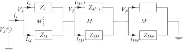
The PEEC method is able solve quasi-static electromagnetic problems by coupling circuit and field components, utilizing the integral forms of Maxwell equations. Generally, the three-dimensional geometries are converted into circuit elements: resistances, self and mutual inductances, and capacitances. Each conductor is discretized according to the chosen mesh, and its resistance, self-inductances, and mutual inductances are computed. The self- and mutual inductances determine the current distribution among the subconductors. The resultant current density allows computing the ac resistance of the entire conductor using a matrix definition of Kirchhoff’s laws. This approach, limited to a single conductor and two parallel rectangular conductors was first proposed in [34], and was generalized to a matrix form for any number of conductors in [37]. The choice of conductor discretization can be done in an adaptive form at a certain frequency, and then the same discretization rule is kept for all frequencies of interest. Assuming a general coil, the PEEC matrix is given by:
A −Z
Y AT
v i
=
vs
is
, (1)
where A is the connectivity matrix that ensures identical currents in all series-connected conductors; Z is the impedance matrix that includes the resistance and self- and mutual- inductances of each subconductor; Y is the admittance matrix consisting of the node capacitances; v is the node voltages vector; iis the branch currents vector; andvs and is are the voltage and current sources for the model excitations [44].
Considering the magneto-quasi-static case, the capacitances submatrix is omitted [36, 37, 46], and the PEEC system matrix becomes
A
M N×N −ZM N×M N
(0)N×N ATN×M N
vN×1
iM N×1
=
⎛
⎝ (0)M Nis ×1 (0)(N−1)×1
⎞
⎠, (2)
whereM is the number of subconductors, to which each conductor is divided, and N is the number of turns of the coil.
Next the derivation of the connectivity matrix A is presented, using a circuit representation for a general set of coils, which is given in Fig. 2. The derivation of impedance matrix Zis presented in the next section. The shown representation can be applied to any set of coils, including a single layer solenoid coil, a flat coil, or a thick solenoid coil.
Identical currents for all N turns are guaranteed by the series connection of the branches, as shown in Fig. 2. The impedance representations in Fig. 2 include both the subconductor resistance and its self-inductance. Note that there are mutual inductances between each subconductor to all other subconductors. Equation (2) can be understood in the following manner: for thejth turn, Kirchhoff’s Voltage Law requires that the voltage across the turn is
Vj−Vj+1=ZjjIj+ M
i=1,i=j
whereZjj represents the DC resistance in series with the self-inductance of the jth turn; Zji represents
the mutual inductance between the jth and ith subconductors; II represents the current through the
ith subconductor. Kirchhoff’s Current Law requires that
M
i=1
Ij,i= M
i=1
Ij+1,i. (4)
As an example, letN = 3 andM = 2. The connectivity matrixAM N×N is represented by
AM N×N =
⎛ ⎜ ⎜ ⎜ ⎜ ⎜ ⎝
1 −1 0
1 −1 0
0 1 −1
0 1 −1
0 0 1
0 0 1
⎞ ⎟ ⎟ ⎟ ⎟ ⎟ ⎠. (5)
The first two rows produceV1−V2; the next two rows produceV2−V3; the last two rows produceV3−0,
since the 3rd conductor is connected to ground. TheZ-matrix is given by
ZMN×MN = ⎛
⎝ Z1,1... . . . Z. .. 1,6... Z6,1 . . . Z6,6
⎞
⎠. (6)
Adding the other matrices and vectors of Eq. (2), we obtain theN ×M+N equations in Eq. (7) ⎛ ⎜ ⎜ ⎜ ⎜ ⎜ ⎜ ⎜ ⎜ ⎜ ⎜ ⎜ ⎜ ⎜ ⎝
1 −1 0 −Z1,1 −Z1,2 −Z1,3 −Z1,4 −Z1,5 −Z1,6
1 −1 0 −Z2,1 −Z2,2 −Z2,3 −Z2,4 −Z2,5 −Z2,6
0 1 −1 −Z3,1 −Z3,2 −Z3,3 −Z3,4 −Z3,5 −Z3,6
0 1 −1 −Z4,1 −Z4,2 −Z4,3 −Z4,4 −Z4,5 −Z4,6
0 0 1 −Z5,1 −Z5,2 −Z5,3 −Z5,4 −Z5,5 −Z5,6
0 0 1 −Z6,1 −Z6,2 −Z6,3 −Z6,4 −Z6,5 −Z6,6
0 0 0 1 1 0 0 0 0
0 0 0 −1 −1 1 1 0 0
0 0 0 0 0 −1 −1 1 1
⎞ ⎟ ⎟ ⎟ ⎟ ⎟ ⎟ ⎟ ⎟ ⎟ ⎟ ⎟ ⎟ ⎟ ⎠ ⎛ ⎜ ⎜ ⎜ ⎜ ⎜ ⎜ ⎜ ⎜ ⎜ ⎜ ⎝ v1 v2 v3 i1 i2 i3 i4 i5 i6 ⎞ ⎟ ⎟ ⎟ ⎟ ⎟ ⎟ ⎟ ⎟ ⎟ ⎟ ⎠ = ⎛ ⎜ ⎜ ⎜ ⎜ ⎜ ⎜ ⎜ ⎜ ⎜ ⎜ ⎝ 0 0 0 0 0 0 is 0 0 ⎞ ⎟ ⎟ ⎟ ⎟ ⎟ ⎟ ⎟ ⎟ ⎟ ⎟ ⎠ (7)
The general procedure for deriving the PEEC connectivity matrix is now given. In general, the connectivity matrixA which is a part of the PEEC matrix in Eq. (2) is defined as
AM N×N =
⎛ ⎜ ⎜ ⎜ ⎜ ⎜ ⎜ ⎜ ⎜ ⎜ ⎜ ⎜ ⎜ ⎜ ⎜ ⎜ ⎜ ⎜ ⎜ ⎜ ⎜ ⎜ ⎜ ⎜ ⎜ ⎜ ⎜ ⎜ ⎜ ⎝ N ⎧ ⎪ ⎪ ⎪ ⎪ ⎪ ⎪ ⎪ ⎪ ⎪ ⎪ ⎪ ⎪ ⎪ ⎪ ⎪ ⎪ ⎪ ⎪ ⎪ ⎪ ⎪ ⎪ ⎪ ⎪ ⎪ ⎪ ⎪ ⎪ ⎨ ⎪ ⎪ ⎪ ⎪ ⎪ ⎪ ⎪ ⎪ ⎪ ⎪ ⎪ ⎪ ⎪ ⎪ ⎪ ⎪ ⎪ ⎪ ⎪ ⎪ ⎪ ⎪ ⎪ ⎪ ⎪ ⎪ ⎪ ⎪ ⎩ M ⎧ ⎪ ⎪ ⎪ ⎪ ⎨ ⎪ ⎪ ⎪ ⎪ ⎩ N
1 −1 0 N. . .−2 0
.. .
1 −1 0 N. . .−2 0
M ⎧ ⎪ ⎪ ⎪ ⎪ ⎨ ⎪ ⎪ ⎪ ⎪ ⎩ N
0 1 −1 0 N. . .−3 0
.. .
0 1 −1 0 N. . .−3 0
.. . M ⎧ ⎪ ⎪ ⎪ ⎪ ⎨ ⎪ ⎪ ⎪ ⎪ ⎩ N
0 N. . .−1 0 1
.. .
0 N. . .−1 0 1
Figure 2. A general model for anN-turn coil and M mesh cells for each turn of the coil.
The vector of node voltages and branch currents is defined as
vN×1
iM N×1
=
⎛ ⎜ ⎜ ⎜ ⎜ ⎜ ⎜ ⎜ ⎜ ⎜ ⎜ ⎝
v1
v2
.. . vN
i1
i2
.. . iM N
⎞ ⎟ ⎟ ⎟ ⎟ ⎟ ⎟ ⎟ ⎟ ⎟ ⎟ ⎠
(9)
The source voltage equals v1 (Fig. 2), so the ac resistance of the coil at 2D or at unity length cross
section is computed as
Rac = Re
⎛
⎝ AM N×N −ZM N×M N
(0)N×N ATN×M N
−1⎛
⎝ (0)M Nis ×1 (0)(N−1)×1
⎞ ⎠
⎞ ⎠
first element of the vector
(10)
withis= 1 A.
The ac resistance factor of the coil is computed by,
Rac,f actor =Rac/Rdc, (11)
whereRdc is the unity length cross section dc resistance of the coil,
Rdc = l
σwxwyN
(12)
andσ is the wire conductivity;wx andwy are the width and height of the wire; andN is the number of
turns. Once the ac resistance factor is determined, the total ac resistance of the coil is computed using
Rac,T = lT
σwxwyRac,f actor,
(13)
wherelT is the total length of the coil. In addition, the distancer from the origin to the spiral is given
by
r =a+bθ,
wherea is the starting point,b the turn pitch divided by 2π, andθ the angle. Finally, the quantity lT
is given by
lT = θ2
θ1
r2+
dr dθ
2
3. Z-MATRIX COMPUTATION
The computation of the Z-matrix can be done in two ways. One is to perform a numeric self and mutualinductance computation, as proposed in [37], and the other, which is based on analytic formulas, is proposed in this paper. The analytic approach requires less computational effort, and hence results in faster computation times.
The conductors in a coil cross section are divided into M subconductors, which are the mesh cells of the problem. The self-resistance, partial self-inductance, and mutual inductances are then computed for each subconductor. The underlying assumption of the PEEC method is that the current is uniform for each subconductor. Therefore, the resistance of each subconductor is computed as its dc resistance
Rsub i,j =
1 σ
l
ab, (15)
wherel is the unity length of the subconductor, andab is its cross section area. The resistances of the subconductors (along with the self-inductances, multiplied by the angular frequency)are placed along the main diagonal of the Z-matrix. The self-inductance of each subconductor is computed using the formula [47, 48], which is
L= μ0l 2π ln 2l GM D
−1 +GM D l
. (16)
The variable GMD is the Geometric Mean Distance, which is given for the rectangular subconductor in [49] by
lnGM D = 1
2ln
a2+b2− 1 12
a2 b2 ln
1 + b
2 a2 −1 12 b2
a2ln
1 + a
2 b2 +2 3 a btan
−1 b
a+ 2 3 b atan
−1 a
b − 25
12, (17)
where a and b are the width and height of the subconductor. The mutual inductance between the rectangular subconductors is computed using the formula for two filaments [48, 50],
M = μ0l 2π ln l d+ 1 + l
2
d2
−
1 +d
2
l2 +
d l
, (18)
withdequal to the spacing between the filaments. The impedance matrix is constructed at the frequency of interest employing Eqs. (15), (16), and (18), where the mutual-inductance terms, multiplied by the angular frequency, populate off-main-diagonal entries of the impedance matrix. It is found in this work that the following mesh size
dx= max (2,2×round (wx/δ)),
dy = max (2,2×round (wy/δ)),
(19)
is adequate, wheredx and dy are the mesh sizes in x and y directions respectively; wx and wy are the
width and height of the conductor, respectively; andδ is the skin depth at the frequency of interest. A finer mesh has a minor impact on accuracy.
4. SIMULATION RESULTS
In this section we first show the match between the method proposed in this paper and the previous method [37], and then show the optimal coil designs. It is shown that the proposed method accurately predicts the results for the Rac factor obtained by the exact 2D method, while requiring significantly
(a) (b)
Figure 3. (a) The coil used for the ac resistance factor computation. The inner radius is 20 mm, the conductor width is 1 mm, the conductor thickness is 35µm, and spacing between the conductors is 0.1 mm. (b) The percentage difference between the analytic method and the method of [37] for the Rac,factor on the test case of a flat spiral coil.
(a) (b)
(c) (d)
the frequency of interest. At low frequencies the proximity effect is negligible, so the spacing should be kept minimal, based on the manufacturing technology limits. However, at higher frequencies, the ac resistance is affected by two opposing factors, namely, the proximity effect and the dc resistance. As the spacing increases, the impact of the proximity effect is decreased, however, the coil length is increased, and hence its dc resistance is increased as well. Therefore, for each frequency and wire dimensions there exists an optimal spacing that minimizes the ac resistance of the coil.
(a) (b)
Figure 5. Results for foil wound coils with inner radius of 20 mm and the foil thickness of 0.2 mm; the number of turns is 10. (a) The ac resistance and (b) the ac resistance factor.
(a) (b)
(c)
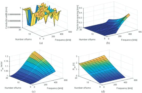
Figure 4 shows the optimization results of a flat spiral coil that is 35µm thick. The upper bound of the optimization for the conductor width is set at 1 mm, and it can be seen that the ac resistance is minimized for this upper bound. However, the optimal turn-to-turn spacing varies as function of frequency and number of turns. While at lower frequencies, the spacing approaches its lower bound, at higher frequencies, and at lower number of turns, the optimal spacing increases.
An additional widely used coil topology employs a copper foil. The proposed method can optimize its overall ac resistance, by varying the foil thickness and turn-to-turn spacing. At first, we consider a coil with thickness of 0.2 mm, with 10 turns. The lower bound on the turn-to-turn spacing is set to 0.1 mm, and the optimizer finds that the spacing should be kept at this minimum at the considered frequency band, up to 40 kHz. The ac resistance and the ac resistance factor are shown in Figs. 5(a) and (b) respectively, as function of foil width. Except for very small foil widths, it can be seen that an increase in foil width only marginally reduces the overall ac resistance, due to the increase of ac resistance factor. This effect is caused by current crowding around the edges of the foil, and very low current density in the central areas.
Since increasing the foil width does not significantly reduce the ac resistance, an additional simulation is done with a thicker foil of 0.5 mm. Such foil thickness is still less than twice the skin depth of copper at 40 kHz.
The simulation results are shown in Fig. 6. It can be seen that the optimal turn-to-turn spacing is kept at the minimum for most of the sweep space, except for smaller foil widths at higher frequencies, as shown in Fig. 6(a). It can be seen that the overall ac resistance of this thicker foil is not necessarily lower than that of 0.2 mm foil, especially for wide foils at high frequencies (Fig. 6(b)). This is due to increased ac resistance factors (Fig. 6(c)) and increased overall copper lengths.
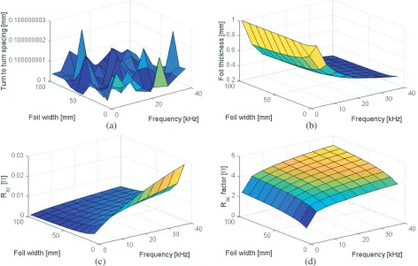
Based on the results of Figs. 5 and 6, the optimization of the foil thickness along with the
turn-to-(a) (b)
(c) (d)
turn spacing is performed. Fig. 7 suggests that optimal turn-to-turn spacing (Fig. 7(a)) is at the lower bound of 0.1 mm, while the optimal foil thickness (Fig. 7(b)) decreases with increasing frequency and with increasing foil width. Figs. 7(c) and (d) present the total ac resistance and the ac resistance factor of this 10 turn coil.
Figure 8. CST simulation of a foil wound coil. The inner radius is 20 mm, the foil thickness is 0.2 mm, the foil width is 10 mm, the turn-to-turn spacing is 0.1 mm, and the number of turns is 10.
(a) (b)
(c) (d)
The proposed method is verified by a standard commercial FEM software — CST EM studio. The chosen test case for the verification is a 10 turn coil made with foils with a foil thickness of 0.2 mm, a foil width of 10 mm, and a turn-to-turn spacing of 0.1 mm. The CST cannot directly compute the ac resistance, and instead computes solid losses. At the considered simulation the excitation current is set to 1 A rms, hence the resulted loss in Watts is identical to ac resistance in ohms. At 40 kHz, the CST computed an ac resistance of 0.0347 Ω, as shown in Fig. 8, which matches the Matlab computed resistance of 0.0325 Ω (Fig. 5).
The additional coil topology, widely employed in high frequency applications, is a single layer solenoid. In this work we consider a solenoid coil wound using edge winding method.
The proposed optimization can minimize its overall ac resistance, by varying the conductor thickness and turn to turn spacing for given conductor width. The considered coil has N = 10 turns. Fig. 9(a) suggests that optimal conductor thickness is at the upper bound of 1 mm, while the optimal turn to turn spacing gradually increases with frequency and conductor width, as shown in Fig. 9(b). Figs. 9(c) and (d) present the total ac resistance and the ac resistance factor of this 10 turn coil.
The proposed method is verified by a standard commercial FEM software — CST EM studio for the test case of a conductor width of 3 mm at 400 kHz, as shown in Fig. 10. The CST computed an ac resistance of 0.0365 Ω, which matches the Matlab computed resistance of 0.034 Ω (Fig. 9).
Figure 10. CST simulation of a single layer solenoid. The inner radius is 20 mm, the conductor width is 3 mm, the conductor height is 1 mm, the turn-to-turn spacing is 20 mm, and the number of turns is 10.
Table 1.
Coil topology and frequency
Simulation time in CST
Simulation time in Matlab (proposed
method)
Simulation time in Matlab (the method
of [37])
Number of tetrahedra in CST
Number of cells in
Matlab
Foil inductor (Fig. 8). Foil thickness is 0.2 mm
Foil height is 10 mm Turn-to-turn spacing is 0.1 mm
Number of turns is 10 Inner radius is 20 mm Frequency is 40 kHz
8 minutes 1.135 seconds 9.949 seconds 192580 1220
Single layer solenoid (Fig. 10). Wire width is 3 mm Wire thickness is 1 mm Turn-to-turn spacing is 20 mm
Number of turns is 10 Inner radius is 20 mm Frequency is 400 kHz
15 minutes 102 seconds 9.5 minutes 213362 10830
5. CONCLUSION
High frequency magnetic devices are increasingly employed in electronic circuits, ranging from transformers, wireless power transfer, and inductors. The proximity effect that influences the ac resistance of these devices often determines the efficiency of the entire electronic system. In this light, this paper proposes a fast numeric method that enables fast optimization of a required magnetic component. The proposed method requires no special commercial software, and can be easily implemented in Matlab.When compared to a previous method [37], we find that the error is below 0.25% over a wide frequency band.
The ac resistance calculation is based on the PEEC method, which solves quasi-static electromagnetic problems by coupling circuit and field components, utilizing the integral forms of Maxwell equations. The three-dimensional geometries are converted into circuit elements that include resistances and partial inductances. Each conductor is discretized according to the chosen mesh, and its resistance, self-inductances, and mutual inductances are computed. The self- and mutual inductances determine the current distribution among the subconductors. The resulting current density allows computing the ac resistance of the entire conductor using a matrix definition of Kirchhoff’s laws. The self and mutual inductances are computed using analytic formulas, which results in very low computational effort.
The proposed method is used to minimize ac resistance of number of coil topologies. The optimization confronts the tradeoffs imposed by conductor geometry, spacing, and total coil length and is demonstrated with number of air core inductor topologies. The results of the proposed method are compared toa standard commercial FEM tool, CST EM studio, and the results match well. This allows a designer to evaluate the ac resistance in a simple way, enabling to reduce the amount of copper used.
REFERENCES
1. Kim, H. J., J. Park, K. S. Oh, J. P. Choi, J. E. Jang, and J. W. Choi, “Near-field magnetic induction MIMO communication using heterogeneous multipole loop antenna array for higher data rate transmission,” IEEE Transactions on Antennas and Propagation, Vol. 64, No. 5, 1952–1962, 2016.
2. Bauernfeind, T., K. Preis, W. Renhart, O. B´ır´o, and M. Gebhart, “Finite element simulation of impedance measurement effects of NFC antennas,”IEEE Trans. Magnetics, Vol. 51, No. 3, 2015. 3. Hong, S., S. Lee, S. Jeong, D. H. Kim, J. Song, H. Kim, and J. Kim, “Dual-directional near field
communication tag antenna with effective magnetic field isolation from wireless power transfer system,” IEEE Wireless Power Transfer Conference (WPTC), 1–3, 2017.
4. Sharma, A., G. Singh, D. Bhatnagar, I. J. Garcia Zuazola, and A. Perallos, “Magnetic field forming using planar multicoil antenna to generate orthogonal H-field components,”IEEE Transactions on Antennas and Propagation, Vol. 65, No. 6, 2906–2915, 2017.
5. Chung, Y. D., C. Y. Lee, D. W. Kim, H. Kang, Y. G. Park, and Y. S. Yoon, “Conceptual design and operating characteristics of multi-resonance antennas in the wireless power charging system for superconducting MAGLEV train,” IEEE Transactions on Applied Superconductivity, Vol. 27, No. 4, 2017.
6. Yodogawa, S. and M. Morishita, “Wireless power transfer system using a Helmholtz coil for electromagnetic suspension carrier system,”19th International Conference on Electrical Machines and Systems (ICEMS), 1–4, 2016.
7. Tuethong, P., P. Yutthagowith, and S. Maneerot, “Design and construction of a variable air-core inductor for lightning impulse current test on surge arresters,”33rd Int. Conf. Lightning Protection (ICLP), 1–4, 2016.
8. Akagi, T., S. Abe, M. Hatanaka, and S. Matsumoto, “An isolated dc-dc converter using air-core inductor for power supply on chip applications,” IEEE Int. Telecomm. Energy Conf. (INTELEC), 1–6, 2015.
9. Barrera-Cardenas, R., T. Isobe, and M. Molinas, “Optimal design of air-core inductor for medium/high power dc-dc converters,” IEEE 17th Workshop on Control and Modeling for Power Electronics (COMPEL), 1–8, 2016.
10. Liang, W., L. Raymond, and J. Rivas, “3-D-printed air-core inductors for high-frequency power converters,” IEEE Trans. Power Electron., Vol. 31, No. 1, 52–64, 2016.
11. Naayagi, R. T. and A. J. Forsyth, “Design of high frequency air-core inductor for DAB converter,”
IEEE Int. Conf. Power Electron., Drives and Energy Systems (PEDES), 1–4, 2012.
12. Nour, Y., M. Orabi, and A. Lotfi, “High frequency QSW-ZVS integrated buck converter utilizing an air core inductor,”IEEE Annual Applied Power Electron. Conf. (APEC), 1319–1323, 2012. 13. Meere, R., N. Wang, T. O’Donnell, S. Kulkarni, S. Roy, and S. Cian O’Mathuna,
“Magnetic-core and air-“Magnetic-core inductors on silicon: a performance comparison up to 100 MHz,” IEEE Trans. Magnetics, Vol. 47, No. 10, 4429–4432, 2011.
14. Dowell, P. L., “Effects of eddy currents in transformer windings,”Proceedings of the Institution of Electrical Engineers, Vol. 113, No. 8, 1387–1394, 1966.
15. Perry, M. P., “Multiple layer series connected winding design for minimum losses,” IEEE Trans. Power Apparatus Syst., Vol. 96/98, No. 1, 116–123, Jan./Feb. 1979.
16. Bennet, E. and S. C. Larson, “Effective resistance of alternating currents of multilayer windings,”
Trans. Amer. Inst. Elect. Eng., Vol. 59, 1010–1017, 1940.
17. Vandelac, J. P. and P. D. Ziogas, “A novel approach for minimizing high frequency effects in high-frequency transformers copper losses,” IEEE Trans. Power Electron., Vol. 3, No. 3, 266–276, Jul. 1988.
18. Ferreira, J. A., “Improved analytical modelling of conductive losses in magnetic components,”
IEEE Trans. Power Electron., Vol. 9, No. 1, 127–131, Jan. 1994.
Mar. 2000.
20. Hurley, W. G. and M. C. Duffy, “Calculation of self and mutual impedances in planar sandwich inductors,” IEEE Trans. Magn., Vol. 33, No. 3, 2282–2290, May 1997.
21. Urling, A. M., et al., “Characterizing high frequency effects in a transformer windings — A guide to several significant articles,” Proc. Appl. Power. Electron. Conf., 373–385, Mar. 1989.
22. Skutt, G. R. and P. S. Venkatraman, “Analysis and measurement of high frequency effects in high-current transformers — A comparison between analytical and numerical solutions,” Appl. Power Electron. Conf., Los Angeles, CA, Mar. 1990.
23. Severns, R., “Additional losses in high-frequency magnetics due to non ideal field distributions,”
Proc. Appl. Power Electron. Conf., 333–338, Boston, MA, Feb. 1992.
24. Robert, F., P. Mathys, and J. P. Schauwers, “Ohmic losses calculation in SMPS transformers: Numerical study of Dowell’s approach accuracy,” IEEE Trans. Magn., Vol. 34, No. 4, 1255–1257, Jul. 1998.
25. Robert, F., P. Mathys, B. Velaerts, and J. P. Schauwers, “Two-dimensional analysis of the edge effect field and losses in high-frequency transformer foils,” IEEE Trans. Magn., Vol. 41, No. 8, 2377–2383, Aug. 2005.
26. Lotfi, A. W. and F. C. Lee, “Two dimensional field solutions for high frequency transformer windings,”Proc. Virginia Power Electron. Conf., 1098–1104, 1993.
27. Zwysen, J., R. Gelagaev, J. Driesen, S. Goossens, K. Vanvlasselaer, W. Symens, and B. Schuyten, “Multi-objective design of a close-coupled inductor for a three-phase interleaved 140 kW dc-dc converter,” 39th IECON, Vienna, 1056–1061, 2013.
28. Lotfi, A. W. and F. C. Lee, “Two-dimensional skin effect in power foils for high-frequency applications,” IEEE Trans. Magn., Vol. 31, No. 2, 1003–1006, Mar. 1995.
29. Robert, F., P. Mathys, and J.-P. Schauwers, “A closed-form formula for 2-D ohmic losses calculation in SMPS transformer foils,” IEEE Trans. Power Electron., Vol. 16, No. 3, 437–444, May 2001. 30. Hu, J. and Ch. R. Sullivan, “The quasi-distributed gap technique for planar inductors: Design
guidelines,”IEEE Ind. Appl. Conf., New Orleans, LA, 1997.
31. Boggetto, J. M., Y. Lembeye, J. P. Ferrieux, and J. P. Keradec, “Copper losses in power integrated inductors on silicon,”Proc. 37th IAS Annu. Conf., 977–983, 2002.
32. Reatti, A. and M. K. Kazimierczuk, “Comparison of various methods for calculating the ac resistance of inductors,”IEEE Trans. Magn., Vol. 38, No. 3, 1512–1518, May 2002.
33. Wang, N., T. O’Donnell, and C. O’Mathuna, “An improved calculation of copper losses in integrated power inductors on silicon,” IEEE Trans. Power Electron., Vol. 28, No. 8, 3641–3647, 2013.
34. Barr, A. W., “Calculation of frequency-dependent impedance for conductors of rectangular cross section,”AMP J. Technology, Vol. 1, 91–100, 1991.
35. Zhang, R., J. White, and J. Kassakian, “Fast simulation of complicated 3-d structures above lossy magnetic media,” IEEE Trans. Magn., Vol. 50, No. 10, 1–16, Oct. 2014.
36. Rosskopf, A., E. Baer, C. Joffe, and C. Bonse, “Calculation of power losses in litz wire systems by coupling FEM and PEEC method,”IEEE Trans. Power Electron., Vol. 31, No. 9, 6442–6449, 2016.
37. Kovacevic-Badstubner, I., R. Burkart, C. Dittli, A. Musing, and J. W. Kolar, “Fast method for the calculation of power losses in foil windings,” Proceedings of the 17th European Conference on Power Electronics and Applications (ECCE Europe 2015), Geneva, Switzerland, Sep. 8–10, 2015. 38. Davies, J. and P. Silvester, “Finite elements in electromagnetics: A jubilee review,”Appl. Comput.
Electromagn. Soc. J., Vol. 9, 10–24, 1994.
39. MAXWELL, 2D&3D Field Simulator, Ansys Corp.
40. CST EM STUDIO, 3D field simulator, CST Computer Simulation Technology GmbH.
41. Zienkiewicz, O. C. and R. L. Taylor, The Finite Element Method Set, 6th Edition, Butterworth-Heinemann, London, U.K., 2005.
43. Lupi, S., F. Dughiero, E. Baake, and J. Lavers, “State of the art of numerical modeling for induction processes,”COMPEL — The Int. J. Comput. Math. Electr. Electron. Eng., Vol. 27, No. 2, 335–349, 2008.
44. Ruehli, A. E., “Equivalent circuit models for three dimensional multiconductor systems,” IEEE Trans. Microw. Theory Tech., Vol. 22, No. 3, 216–221, 1974.
45. Tran, T.-S., G. Meunier, P. Labie, and J. Aime, “Comparison of FEM-PEEC coupled method and finite-element method,”IEEE Trans. Magn., Vol. 46, No. 4, 996–999, Apr. 2010.
46. Larsson, J., “Electromagnetics from a quasistatic perspective,” Am. J. Phys., Vol. 75, 230–239, 2007.
47. Strunsky, B. M., “Short electric network of electric furnaces,”GN-TIL, Moscow, 1962.
48. Paul, C. R.,Introduction to Electromagnetic Compatibility, John Wiley & Sons Inc, Hoboken, New Jersey, 2006.
49. Magnusson, P. C., “Geometric mean distances of angle-shaped conductors,” Transactions of the American Institute of Electrical Engineers, Vol. 70, No. 1, 121–123, 1951.