Simulation-Driven Design for a Hybrid Lumped and Distributed
Dual-Band Stub Using Input and Output Space Mapping
Jianqiang Gong*, Yuhao Wang, and Chaoqun Zhang
Abstract—In this paper, a dual-band stub (DBS) comprising one lumped kernel circuit unit cell (KCUC) and two distributed uniform transmission lines is presented. An odd-even mode resonant frequency ratio (OEMRFR) is introduced, which can determine all the element values in the DBS circuit model. Its phase and impedance bandwidth properties are extracted based on the image parameter theory. By adjusting the OEMRFR value, the second working bandwidth and structural size can be controlled simultaneously. On the other hand, the input and output space mapping (IOSM) is exploited to realize a planar microstrip DBS by transferring the lumped KCUC into a quasi-lumped formation. The established ISOM design process is fully automated and can generate the finalized DBS layout with just a few full-wave simulations. A DBS operative at WLAN dual frequencies of 2.4/5.8 GHz with extended bandwidth is designed as an example. Good agreement between the measured and simulated results justifies both the extracted dual-band performance of the proposed DBS and its customized IOSM design process.
1. INTRODUCTION
Multi-band stubs (MBSs) always possess specific characteristic impedances and ±90◦ phase shifts at several operating frequencies, being crucial in the development of advanced dual-band or multi-band microwave components, such as impedance transformers, power dividers, hybrid couplers, filters, and antennas. Over the past years, quite a few MBSs have been put forward and widely applied in the design of multi-band devices. In [1] and [2], the nonresonant-type composite right/left-handed (CRLH) transmission line (TL) by using surface mounted devices (SMDs) has been used to replace the quarter-wave (λ/4) sections in traditional branch-line couplers, in order to realize dual frequencies or dual modes operation. Correspondingly, resonant-type CRLH TL loaded with complementary split-ring resonators (CSRRs) was also utilized to design multi-band couplers, power splitters and bandpass filters [3–5]. Both the nonresonant-type and resonant-type CRLH TLs belong to the dispersion engineering realm [6], in which the dispersive phase shift and Bloch impedance properties of the artificial TLs can be tailored to develop multi-band devices [1–8]. Another mainstream design concept is the network equivalence, in which the network parameters of the proposed MBS are forced to be equivalent to those of the conventional uniform TL [9–13]. In [9], explicit design formulas for a Π-shaped dual-band stub (DBS) were derived by comparing its transfer function matrix to that of a uniform 90◦ TL, while in [10] and [11], two-section C-type coupled line can realize a dual-band chebyshev impedance transformer or a quad-frequency impedance transformer, respectively. A T-section coupled lines network was utilized as a quad-band impedance inverter to design a quad-band Doherty power amplifier [12]. In [13], two T-shaped DBSs are cascaded to construct 180◦ dual-band phase shifter, being a key element in an improved 3 dB dual-band directional coupler. In brief, dispersion engineering and network equivalence are the two major design ideas for constructing MBSs.
Received 14 October 2018, Accepted 28 November 2018, Scheduled 4 December 2018
* Corresponding author: Jianqiang Gong ([email protected]).
In this paper, we focus on investigating the phase and impedance bandwidths’ properties as well as the fast implementation technique for a novel DBS. The DBS comprises one lumped kernel circuit unit cell (KCUC) and two uniform TLs touching the two terminals of the KCUC. Both major design ideas summarized above are invoked to analyze its performance. Based on the network equivalence method, an odd-even-mode resonant frequency ratio (OEMRFR) is introduced to determine all the DBS element values, being also a key parameter to guarantee the DBS’s element realizability and size reduction. Through analyses with image parameter method in the dispersion engineering realm, it is quite interesting to find that the OEMRFR can regulate the DBS phase and impedance bandwidths’ properties. A smaller OEMRFR will generate a substantially enlarged working bandwidths at the second passband, only compromised by some little loss in size reduction. These excavated characteristics can offer valuable guidelines to design the DBS based multi-band miniature microwave components with improved bandwidth performance.
By transferring the lumped KCUC into planar microstrip quasi-lumped elements, the input and output space mapping (IOSM) technique is employed to acquire the DBS’s optimal layout, in which the surrogate model is the calibrated low-cost purely analytical coarse model (CM), while the fine model (FM) is the high-fidelity full-wave model. The presented IOSM process is fully automated, incorporating optimizable dimensions’ initialization, key step of parameter extraction and reoptimization of the surrogate model [14].
2. DBS WITH EXTENDED BANDWIDTH
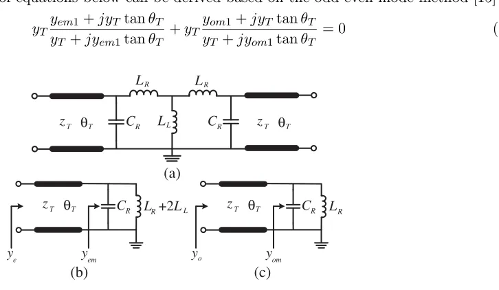
Figure 1 shows the DBS two-port circuit model and the corresponding even-/odd-mode single-port equivalent circuits. Each TL segment is featured by the characteristic impedance zT and the electrical lengthθT, while the KCUC is configured with series inductorLR, shunt inductorLLand shunt capacitor
CR. The input admittance for even-mode single-port is
ye=yTyyem+jyT tanθT
T +jyemtanθT (1)
withyem= (ω2em−ω2)CR/jωandωem= 1/(LR+ 2LL)CR, whereyemis the terminal load admittance,
ωem the parallel resonant frequency of yem, and yT = 1/zT. yo,yom and ωom for odd-mode single-port circuit have similar definitions. Key parameter OEMRFR is defined as
n=ωom/ωem =1 + 2LL/LR (2)
If the DBS is to realize characteristic impedance z with electrical length ±90◦ at ω1 and ω2 respectively, the system of equations below can be derived based on the odd-even-mode method [15]
yTyyem1+jyTtanθT T +jyem1tanθT
+yTyom1+jyT tanθT
yT +jyom1tanθT
= 0 (3)
R
C LL CR
R
L LR
T z
R C
em y
R
L +2L
e y
R C
om y
R L
o y (a)
(b) (c)
θT zT θT
T
z θT zT θT
L
yTyyem1+jyT1tanθT T +jyem1tanθT −yT
yom1+jyT tanθT
yT +jyom1tanθT = 2j
z (4)
yTyyem2+jyT tanmθT T +jyem2tanmθT
+yTyom2+jyT tanmθT
yT +jyom2tanmθT
= 0 (5)
yTyyem2+jyT tanmθT T +jyem2tanmθT −yT
yom2+jyT tanmθT
yT +jyom2tanmθT
=−2j
z (6)
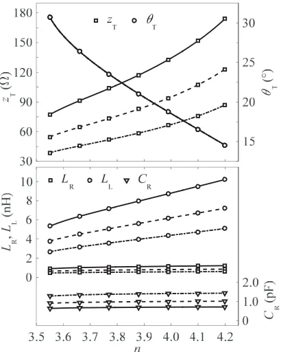
whereyemi andyomiare the admittances atωi(i= 1,2);θT is the electric length atω1; andm=ω2/ω1, being the working frequency ratio. The equation system is stably solved using the trust-region-dogleg algorithm [16]. There will be two sets of solutions by delimitingθT into (5◦, 45◦), and the set of solutions with monotone increasing zT and monotone decreasingθT is of concern, since the circuit compactness matters. Fig. 2 plots the DBS parameter solutions for three different z values as f1 = 2.4 GHz and
f2 = 5.8 GHz. It is observed that θT are all the same for different z with identical n, lying between (14◦, 31◦), and largernleads to smallerθT, being helpful to reduce circuit size. Asn increases,zT and
LL are getting larger, while LR and CR almost remain unchanged. When n is fixed, larger z requires much larger zT, so it becomes harder to realize miniaturized circuit under the larger zcondition, since
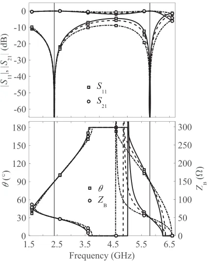
zT cannot be too high for common planar TL types. Fig. 3 shows the S-parameters and the image parameters for the DBS in different z but with unified n. The S-parameters are obtained by using ADS circuit simulator. It is worth noting that for a symmetrical two-port, the image impedance and the propagation factor in the image parameter method match totally with the Bloch impedance and the transfer phase in the periodic theory respectively, being effective tools to clarify the phase and impedance bandwidths’ properties of the DBS [17]. The transfer phaseθand the real part of the image impedanceZB depicted in Fig. 3 are thus defined by
θ = (arccos(A)) (7)
ZB =
B √
A2−1
(8)
where ( ) means extracting real part operation, whereasAandBare the first and second elements of the
Figure 2. DBIT theoretical element values with variation of OEMRFR n. z = 70.71 Ω — real line,
DBS transfer function matrix, respectively, and they can be expressed with the computedS-parameters as
A = 1−S 2 11+S212 2S21
(9)
B = z(1 +S11) 2−S2
21 2S21
(10)
From Fig. 3, it is observed thatθ= 90◦ at the two specified working frequencies, and the transfer phase curve slope versus frequency is positive at f1, presenting a +90◦ phase shift, while it is negative at
f2, manifesting a −90◦ phase shift. With identical n, the transfer phase curves for different z almost completely overlap, and in addition, the absolute image impedance curve slope increases along with
z, but it has little effect on the working bandwidth. Comparably, Fig. 4 shows the same parameters as in Fig. 3 but in different n and with unanimous z. It is clearly seen that the variation of n value has negligible impact on the first working bandwidth, but both the absolute image impedance curve slope and the absolute transfer phase curve slope decrease with n at f2, thus substantially enlarging the second working bandwidth. If the working bandwidth is defined by |S11|<−20 dB, it is 340 MHz (5.62–5.96 GHz) for n = 3.6 case, more than twice larger than 140 MHz (5.73–5.87 GHz) for n = 4.2 case, but meanwhile, the first working bandwidth is always about 535 MHz at both cases. In fact, there is a compromise between the second bandwidth enlargement and the circuit compactness, since smallerncorresponds to larger θT as indicated in Fig. 2. Up to now, two intuitive design guidelines can be summed up: first, the absolute transfer phase curve slope is of the dominant factor to control the working bandwidth other than the absolute image impedance curve slope; second, a rationally chosenn value can assure both the enlarged second bandwidth and the miniaturized circuit size simultaneously.
-60 -50 -40 -30 -20 -10 0 S11 S21
1.5 2.5 3.5 4.5 5.5 6.5
Frequency (GHz) 0 30 60 90 120 150 180 0 50 100 150 200 250 300 ZB
Figure 3. S-parameters and image parameters for DBIT with n= 3.9. z = 70.71 Ω — real line,
z= 50 Ω — dash line andz= 35.35 Ω — dash dot line. -60 -50 -40 -30 -20 -10 0 S11 S21
1.5 2.5 3.5 4.5 5.5 6.5
Frequency (GHz) 0 30 60 90 120 150 180 0 50 100 150 200 250 300 ZB
Figure 4. S-parameters and image parameters for DBIT with z = 50 Ω. n = 4.2 — real line,
3. FAST IMPLEMENTATION OF DBS LAYOUT BASED ON IOSM
Though the proposed DBS is in a hybrid lumped and distributed configuration, if the lumped element
LR, CR and LL in KCUC are transformed into the microstrip high/low-impedance lines and shorted stub, respectively, as shown in Fig. 5, the DBS can be designed in a purely planar structure. IOSM is chosen to achieve the automatic synthesis of the planar DBS, being one of the space mapping (SM) optimization techniques, and its general formulation can be referenced to [14], which we outline here for completeness and better comprehension of the paper. If the original problem is to optimize the high-fidelity EM modelRf(x)
x∗ = arg min
x U(Rf(x)) (11)
whereU is an objective function that encodes given performance specifications;x∗is the optimum design to be found. Instead, we shift the direct optimization burden from Rf to its cheaper representation, the surrogate model. A generic surrogate model scheme can be described as an iterative process
x(i+1) = arg min x U
R(si)(x)
(12)
whereR(si)is a surrogate model often constructed by calibrating physics based low-fidelity CMRc;x(i),
i= 0,1, . . ., is a sequence of approximated solutions to the original problem. Rc can be an analytical model, an equivalent circuit, or even a coarse-discretized EM model, being less accurate but much more computationally efficient than its high-fidelity EM counterpart. In this paper, the surrogate mode that we choose takes the form
R(si)(x) =Rc
x+c(i)
+d(i) (13)
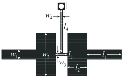
where the input SM vectorc(i) is found by minimizing 2-normRf(x(i))−Rc(x(i)+c), and then, the output SM parametersd(i)is calculated asRf(x(i))−Rc(x(i)+c(i)), ensuring zeroth-order consistency between the surrogate and the FM. In this paper, IOSM is grounded on the well-behaved and fast equivalent circuit CM shown in Fig. 1(a), where all the parameters are formulated with classical empirical formula characterizing microstrip TL and quasi-lumped elements [18]. Good correlations between the CM and the FM will lead to a safe convergence of the process (12) after a few iterations, each requiring just one evaluation of the high-fidelity FM. This, in conjunction with the fact that Rc is much faster thanRf, reduces substantially the overall design cost.
The targeted DBS withz= 50 andn= 3.6 is selected as an example, since it features a substantially enlarged second matching bandwidth as illustrated in Section 2. The objective element values are
z∗
t = 59.5689 Ω, θ∗ = 28.3727◦, L∗R = 0.6941 nH, CR∗ = 0.9301 pF and L∗L = 4.1505 nH, which can be read from Fig. 2. The adopted microstrip substrate has relative permittivity εr of 2.65, loss tangent tanδ of 0.002, and thickness h of 1 mm. In the beginning, eight dimensions as annotated in Fig. 5 are to be initialized. w1 = 2.0671, which is determined byzt∗;w2, w3 and w4 may be chosen arbitrarily if only w2 and w3 can satisfy the microstrip low/high-impedance-line requirements respectively, and w4
1
w
l
12
l
2w
4
w
3
l
3
w
4
l
should be smaller thanl3. To this end, we designate w2 = 9.0 and w3=w4= 0.3. x= [l1, l2, l3, l4] are specified as the optimizable design parameters. The initialx is obtained by minimizingSB−Rc(x), in whichRc(x) are theS-parameters based on the CM, whileSB stand for the benchmarked ones from the circuit simulation with the objective element values. Since loss effects are not included in the FM simulations, either S11 or S21 is enough to construct objective functions throughout the paper. The initialxis promptly solved using the fminunc function with quasi-Newton algorithm in MATLAB [16], and they are x(0)= [6.7736, 3.1043,1.1024,7.9338]. The initial layout parameters are then transferred to ANSYS HFSS to conduct the FM simulation, in which Delta S is set to be 0.005 at the solution frequency of 6 GHz for the fine mesh generation. The evaluated full-wave S-parameters Rf(x(0)) are then returned back to MATLAB to extract c(0) and d(0) as (13) implies. Succeedingly, we reoptimize the surrogate model R(0)s (x) by minimizing SB−R(0)s (x) to generate x(1). Such IOSM process is repeated until the error function (EF) below satisfies
EF = (θ∗−θ)2+LR∗ −LR2+CR∗ −CR2+L∗L−LL2<0.01 (14)
where the element values [θ, LR, CR, LL] are extracted by aligning the S-parameters from circuit simulation withR(fi). During the IOSM process, MATLAB is the master control engine, which guides the IOSM algorithm operated under a fully automatic way, since the FM simulation conducted in ANSYS HFSS can be automatically triggered with MATLAB by virtue of HFSS VBScripting function [19]. After VBScripting programming in HFSS, the generated script file in .vbs format can be linked and executed in MATLAB using the following statement
dos(WScriptdirectory\filename.vbs)
where “WScript” is a certain command in HFSS VBScripting language which can launch .vbs script file using HFSS simulator, and “dos” function in MATLAB allows to execute the external command “WScript” directly.
We also use the constrained interior-point method and unconstrained Nelder-Mead simplex method, two direct optimization algorithms (DOAs) encapsulated into the fmincon and fminsearch functions in MATLAB, respectively [16]. TheS-parameter derivatives with respect to the geometrical variations can be invoked in the fmincon function, which are computed with the adjoint sensitivity technique inherent in HFSS [19]. Both DOAs employ the same EF as SB−Rf(x) during the optimization process. Optimization results are summarized in Table 1, and the EF therein is specified as Eq. (14) to facilitate comparison. The computing platform is a personal computer with Intel I7-4790K CPU and 32 GB RAM. Concerning IOSM, only 9 FM simulations taking up 10.4 minutes are needed to arrive at the final x, while both DOAs consume far more FM simulations and time. Overall, the customized IOSM
Table 1. Optimization results.
IOSM
Finalx= [5.5884, 3.4987, 0.8659, 7.4935]
EF = 0.0098 Elapsed time: 10.4 mins
interior-point algorithm (fmincon)
Finalx= [5.5925, 3.4884, 0.8669, 7.2100]
EF = 0.0767 Elapsed time: 151.9 mins
Nelder-Mead simplex algorithm (fminsearch)
Finalx= [5.4823, 3.5590, 0.8440, 7.2334]
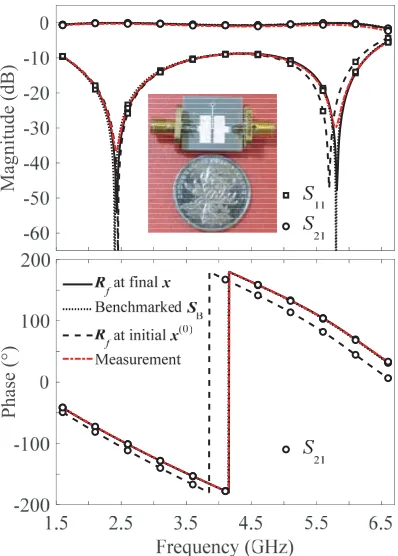
process indeed possesses relatively high efficiency and accuracy compared to the traditional DOAs. As shown in Fig. 6, the FMS-parameters of the optimal microstrip DBS after IOSM optimization coincide perfectly withSB throughout the band of interest. In other words, the distributed microstrip circuit in Fig. 5 can be modelled thoroughly by using the hybrid lumped and distributed circuit in Fig. 1(a), as interesting as work presented in [20], where L-shaped iris embedded in substrate integrated waveguide was able to be modelled completely using a lumped element circuit.
Magnitude (
d
B)
Phase (
°)
Figure 6. S-parameters of microstrip DBIT.
Comparably, S-parameters of the FM with x(0) present obvious misalignment from SB, meaning that further optimization must be carried out. A prototype DBS with the optimized design parameters was further fabricated and tested. The two-port measurement was carried out using the Agilent E5071C network analyzer. For easy comparison, the measured results are superimposed with the simulated ones in Fig. 6, inset with the prototype photo. Very good agreement is achieved, thus verifying the proposed synthesis method finally.
4. CONCLUSION
The phase and impedance bandwidth characteristics for the proposed DBS have been comprehensively disclosed by exerting the image parameter method. Two directive principles for designing the DBS based dual-band microwave devices with improved bandwidth performance have been established. On the other hand, detailed information on applying the IOSM optimization algorithm to realize the specified microstrip DBS has been presented. From the given theoretical specifications to the finalized layout, the proposed automatic synthesis technique demonstrates relatively high efficiency and accuracy. With the deeply uncovered working mechanisms as well as the highly effective optimization technique, we believe that the proposed DBS will find potential applications to design novel compact multi-band devices in stirringly high efficiency.
REFERENCES
1. Lin, I.-H., M. D. Vincentis, C. Caloz, et al., “Arbitrary dual-band components using composite right/left-handed transmission lines,” IEEE Trans. Microw. Theory Tech., Vol. 52, No. 4, 1142– 1149, 2004.
2. Chang, L. and T.-G. Ma, “Dual-mode branch-line/rat-race coupler using composite right-/left-handed lines,”IEEE Microw. Wireless Comp. Lett., Vol. 27, No. 5, 449–451, 2017.
3. Bonache, J., G. Sis´o, M. Gil, et al., “Application of composite right/left handed (CRLH) transmission lines based on complementary split ring resonators (CSRRs) to the design of dual-band microwave components,”IEEE Microw. Wireless Comp. Lett., Vol. 18, No. 8, 524–526, 2008. 4. Dur´an-Sindreu, M., G. Sis´o, J. Bonache, et al., “Planar multi-band microwave components based
on the generalized composite right/left handed transmission line concept,” IEEE Trans. Microw.
Theory Tech., Vol. 58, No. 12, 3882–3891, 2010.
5. Selga, J., A. Rodr´ıguez, V. E. Boria, et al., “Synthesis of split-rings-based artificial transmission lines through a new two-step, fast converging, and robust aggressive space mapping (ASM) algorithm,”IEEE Trans. Microw. Theory Tech., Vol. 61, No. 6, 2295–2308, 2013.
6. Caloz, C., “Metamaterial dispersion engineering concepts and applications,” Proc. IEEE, Vol. 99, No. 10, 1711–1719, 2011.
7. Cao, W.-Q., B. Zhang, A. Liu, T. Yu, D. Guo, and Y. Wei, “Novel phase-shifting characteristic of CRLH TL and its application in the design of dual-band dual-mode dual-polarization antenna,”
Progress In Electromagnetics Research, Vol. 131, 375–390, 2012.
8. Wu, G.-C., G. Wang, L.-Z. Hu, Y.-W. Wang, and C. Liu, “A miniaturized triple-band branch-line coupler based on simplified dual-composite right/left-handed transmission branch-line,” Progress In
Electromagnetics Research C, Vol. 39, 1–10, 2013.
9. Cheng, K.-K. and S. Wong, “A novel dual-band 3-dB branch-line coupler design with controllable bandwidths,”IEEE Trans. Microw. Theory Tech., Vol. 60, No. 10, 3055–3061, 2012.
10. Page, J. E. and J. Esteban, “Dual-band matching properties of the C-section all-pass network,”
IEEE Trans. Microw. Theory Tech., Vol. 61, No. 2, 827–832, 2013.
11. Bai, Y.-F., X.-H. Wang, C.-J. Gao, et al., “Design of compact quad-frequency impedance transformer using two-section coupled line,” IEEE Trans. Microw. Theory Tech., Vol. 60, No. 8, 2417–2423, 2012.
12. Li, X., M. Helaoui, F. Ghannouchi, et al., “A quad-band Doherty power amplifier based on T-section coupled lines,” IEEE Microw. Wireless Comp. Lett., Vol. 26, No. 6, 437–439, 2016.
13. Arigong, B., J. Shao, M. Zhou, H. Ren, J. Ding, Q. Mu, Y. Li, S. Fu, H. Kim, and H. Zhang, “An improved design of dual-band 3 dB 180◦ directional coupler,” Progress In Electromagnetics
Research C, Vol. 56, 153–162, 2015.
15. Hsu, C.-L., J.-T. Kuo, and C.-W. Chang, “Miniaturized dual-band hybrid couplers with arbitrary power division ratios,” IEEE Trans. Microw. Theory Tech., Vol. 57, No. 1, 149–156, 2009.
16. The Mathworks Inc.,MATLAB Optimization Toolbox User’s Guide, Version R2016b, Natick, MA, 2015.
17. Pozar, D. M., Microwave Engineering, 4th Edition, Wiley, Hoboken, 2012.
18. Hong, J. S. and M. J. Lancaster, Microstrip Filters for RF/Microwave Applications, Wiley, New York, 2001.