Electronic Thesis and Dissertation Repository
9-3-2013 12:00 AM
Optical Properties, Electronic Structures and High Pressure Study
Optical Properties, Electronic Structures and High Pressure Study
of Nanostructured One Dimensional Titanium Dioxide by
of Nanostructured One Dimensional Titanium Dioxide by
Synchrotron Radiation and Spectroscopy
Synchrotron Radiation and Spectroscopy
Ankang Zhao
The University of Western Ontario
Supervisor Yang Song
The University of Western Ontario Joint Supervisor Tsun-Kong Sham
The University of Western Ontario Graduate Program in Chemistry
A thesis submitted in partial fulfillment of the requirements for the degree in Master of Science © Ankang Zhao 2013
Follow this and additional works at: https://ir.lib.uwo.ca/etd
Part of the Physical Chemistry Commons
Recommended Citation Recommended Citation
Zhao, Ankang, "Optical Properties, Electronic Structures and High Pressure Study of Nanostructured One Dimensional Titanium Dioxide by Synchrotron Radiation and Spectroscopy" (2013). Electronic Thesis and Dissertation Repository. 1601.
https://ir.lib.uwo.ca/etd/1601
This Dissertation/Thesis is brought to you for free and open access by Scholarship@Western. It has been accepted for inclusion in Electronic Thesis and Dissertation Repository by an authorized administrator of
OPTICAL PROPERTIES, ELECTRONIC STRUCTURES AND HIGH PRESSURE
STUDY OF NANOSTRUCTURED ONE DIMENSIONAL TITANIUM DIOXIDE BY
SYNCHROTRON RADIATION AND SPECTROSCOPY
(Thesis Format: Integrated-Article)
By
Ankang Zhao
Graduate Program in Chemistry
A thesis submitted in partial fulfillment
of the requirements for the degree of
Master of Science
The School of Graduate and Postdoctoral Studies
The University of Western Ontario
London, Ontario, Canada
ii
Abstract
One dimensional (1D) titanium dioxide (TiO2) nanomaterials have been extensively studied
in recent years due to their superior electrical, optical mechanical and chemical properties compared with their bulk counterparts. Two different kinds of 1D TiO2 nanomaterials, TiO2 nanowires (TiO2 NW) and TiO2 nanotubes (TiO2 NT), are studied in this thesis by using various techniques.
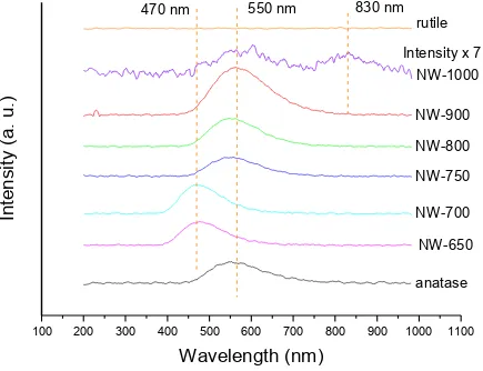
In one study, TiO2 NW synthesized by hydrothermal method and a series of calcinated TiO2 NW were investigated by using absorption near edge structures (XANES), X-ray diffraction (XRD) and X-ray excited optical luminescence (XEOL). It is found that TiO2 NW as synthesized undergo a phase transition under calcination: TiO2-B phase transformed to anatase phase and then to rutile phase. Moreover, a green photoluminescence (PL) started showing up at a wavelength of 470 nm at 650 ℃, then shifts to 550 nm at 750 ℃ and finally at 1000 ℃ the green PL disappears and near infrared (IR) PL was observed. Also optical behaviours are consistent with the phase transformation sequence. The green PL at 550 nm
and near IR PL at 830 nm is attributed to oxygen vacancies of anatase phase and the bulk defects of rutile phase respectively. However, a new phenomenon is observed, the green PL observed at 470 nm. Considering this green PL is consistent with the presence of the TiO2-B phase, it is proposed that the green PL at 470 is due to the TiO2-B phase.
iii
Keywords
iv
The Co-Authorship Statement
I hereby declare that this thesis is written by Ankang Zhao. Dr. Yang Song and Dr.
Tsun-Kong Sham played a major role in the editing and revision of the materials presented in all chapters.
TiO2 nanowires in Chapter 3 were synthesized by Ankang Zhao in the Song laboratory. TiO2 nanotubes in Chapter 4 were provided by Dr. Tsun-Kong Sham’s group in the University of Western Ontario. Besides, Ankang Zhao is responsible for all data collection and analysis.
I am aware of the University of Western Ontario Policy on Authorship and I certify that I have properly acknowledged the contribution of other researchers to my thesis.
v
vi
Acknowledgements
First of all, I would like to express my great gratitude to both of my supervisors, Dr. Yang Song and Dr. Tsun-Kong Sham, for their exceptional supervision, encouragement, and
unconditional support. It has been a great honor for having the opportunity to study and work under the guidance of such great supervisors. Your kindness, passion and enthusiasm always encourage me.
Next, I would like to thank my group members: Dr. Yun-Mui Yiu, Dr. Zhiqiang Wang, Dr. Haiyan Mao, Dr. Dongniu Wang, Ms. Olga Lobacheva, Mr. Xiaoxuan Guo, Mr. Yue Hu, Mr.
Fuyan Zhao, Ms. Dong Zhao, Mr. Liang Zhou, Mr. Zhihao Yu and Mr. Jun Li for their helpful discussion constructive feedback on the ongoing research. And I really appreciate our
former group members, Dr. Zhaohui Dong and Dr. Lijia Liu. You have been providing great help to me since the start of my graduate study.
I appreciate all the technical support by the following people: Dr. Robert Blyth, Mr. Tom
Regier, Mr. David Chevier from Canadian Light Source; Dr. Jesse Smith from Advanced Photon Source; Mr. Todd Simpson from Nanofabrication Laboratory. Their expertise and
willingness to help made my experiments running more smoothly.
I would like thank my friends (Jun Xu, Michael Linda Wu, Peng He, Xiaoxiao Wang, Renjie Hou, Yiyi Liu, Bo Fan). It is you who drive the loneliness away from me and leave me a
colorful and joyful Canadian life.
Finally, I would like to give my special thanks to my parents for their love, unconditional
vii
Table of Contents
Abstract ... ii
The Co-Authorship Statement...iv
Acknowledgements ...vi
Table of Contents ... vii
List of Tables... x
List of Figures ... x
List of Appendix Figures ... xiii
List of Abbreviations ... xiv
Chapter 1 Introduction ... 1
1.1 Titanium dioxide ... 1
1.1.1 Background ... 1
1.1.2 Nanomaterials and TiO2 nanomaterials ... 1
1.1.3 Applications... 4
1.1.4 Synthesis methods of TiO2 NT and NW ... 6
1.2 X-ray absorption and related spectroscopy ... 8
1.2.1 X-ray absorption near-edge structures (XANES) ... 8
1.2.2 X-ray excited optical luminescence (XEOL) ... 10
1.2.3 De-excitation processes following the X-ray absorption ... 12
1.3 High pressure phenomena ... 13
1.3.1 High-pressure study ... 13
1.3.2 High pressure effects on nanomaterials ... 15
1.4 Motivations ... 16
1.5 References... 17
Chapter 2 Instrumentation... 23
2.1 Synchrotron radiation ... 23
2.1.1 Principle of synchrotron radiation ... 23
2.1.2 Synchrotron facilities ... 26
viii
2.2 High pressure techniques ... 28
2.2.1 Diamond anvil cells ... 28
2.2.2 The ruby pressure gauge ... 30
2.2.3 Pressure transmitting medium ... 31
2.3 Raman spectroscopy ... 32
2.4 Other characterization techniques ... 34
2.4.1 Powder X-ray diffraction ... 34
2.4.2 Scanning electron microscope ... 34
2.5. References... 35
Chapter 3 XANES and XEOL studies of TiO2 nanowires ... 36
3.1 Introduction ... 36
3.2 Experimental section ... 37
3.2.1 Sample preparation ... 37
3.2.2 Characterization ... 38
3.3 Results and discussion ... 38
3.3.1 Morphology ... 38
3.3.2 XANES study of calcinated TiO2 NW... 40
3.3.3 XEOL and PLY analysis of calcinated TiO2 NW ... 49
3.4 Conclusions ... 51
3.5 References... 52
Chapter 4 Pressure-induced structural transformations of TiO2 nanotubes by Raman spectroscopy and synchrotron X-ray diffraction ... 54
4.1 Introduction ... 54
4.2 Experimental section ... 57
4.2.1 Sample preparation ... 57
4.2.2 Characterization ... 57
4.3 Results and discussion ... 59
4.3.1 Morphology ... 59
4.3.2 Raman results of TiO2 NT upon compression and decompression ... 60
ix
4.3.4 Discussion ... 66
4.4 Conclusions ... 72
4.5 References... 72
Chapter 5 Summary and future work ... 76
5.1 Summary ... 76
5.2 Future work ... 77
5.3 References... 78
Appendix I Data analysis methods ... 79
A1.1 FIT2D ... 79
A1.2 Rietveld refinement method ... 83
Appendix II Supporting materials for Chapter 4 ... 84
x
List of Tables
Table 4-1 Summary of the results of high-pressure studies of anatase TiO2. ... 71
List of Figures
Figure 1-1 A schematic illustration of bulk material, nanofilm, nanowire and nanopartile.2 Figure 1-2 Schematic illustrations of density of states comparison (a) among bulk, nano and atom, and (b) among bulk and nanomaterials with specific dimensionality... 3Figure 1-3 Light absorption measurements ... 8
Figure 1-4 Log-log plot of the mass absorption coefficient of platinum as a function of X-ray photo energy ... 9
Figure 1-5 Schematic diagram of the electron-hole pair generation and recombination. . 10
Figure 1-6 Decay of the excited state: X-ray fluorescence (left) and the Auger effect (right). ... 12
Figure 1-7 Phase transitions of wurtzite CdSe nanocrystals towards rocksalt structure as a function of the diameter of the crystal.. ... 15
Figure 2-1 Schematic layout of a synchrotron radiation facility ... 23
Figure 2-2 Schematic of a (a) bending magnet, (b) wiggler and (c) undulator. ... 25
Figure 2-3 Opening angle and flux (vs. Ephoton) of (a) bending magnets, (b) wigglers, and (c) undulators. ... 25
Figure 2-4 Schematic layout of the CLS beamlines. ... 26
Figure 2-5 Schematic layout of the APS beamlines. ... 27
Figure 2-6 (a): Side view of an assembled symmetric piston-cylinder type DAC and (b): photo of the dissemble DAC with two parts, piston and cylinder... 29
Figure 2-7 The schematics of a diamond anvil cell ... 30
Figure 2-8 Ruby fluorescence measured at different pressures. ... 31
xi
Figure 2-10 Raman system in the Song Lab ... 34
Figure 3-1 SEM images of as-prepared nanowires and TiO2 NW calcinated for 2h at different temperatures. ... 39
Figure 3-2 Ti L3,2-edge XANES TEY of anatase phase of TiO2 and rutile phase of TiO2 ... 40
Figure 3-3 Ti L3,2-edge XANES TEY of calcinated TiO2 NW ... 41
Figure 3-4 XRD pattern of as-prepared and calcinated TiO2 NW ... 42
Figure 3-5 FLY of Ti L3,2-edge of as-prepared and calcinated TiO2 NW ... 43
Figure 3-6 O K-edge XANES TEY of as-prepared TiO2 NW and TiO2 NW at different calcinated temperatures... 44
Figure 3-7 FLY of O K-edge of as-prepared and calcinated TiO2 NW ... 45
Figure 3-8 XEOL spectra collected with excitation photon energy at 550eV at different temperatures ... 46
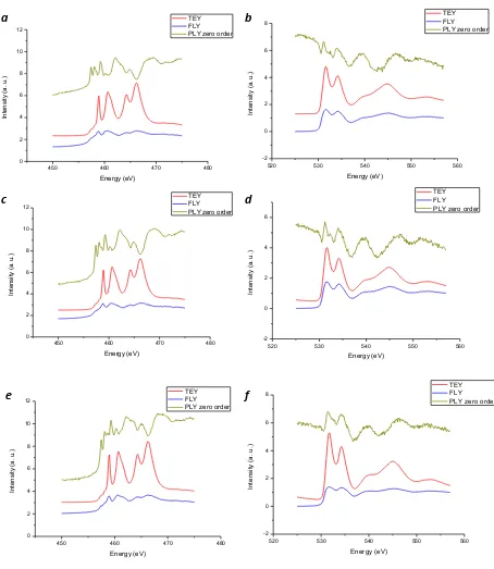
Figure 3-9 PLY-XANES spectra at the Ti L3,2-edge (left) and the O K-edge (right) of (a,b) NW-650, (c,d) NW-700, (e,f) NW-750 ... 47
Figure 3-10 PLY-XANES spectra at the Ti L3,2-edge (left) and the O K-edge (right) of (a,b) NW-800, (c,d) NW-900, (e,f) NW-1000 ... 48
Figure 4-1 Crystal structures of TiO2. a: anatase phase; b: α-PbO2 phase; c: baddeleyite phase ... 55
Figure 4-2 SEM images of anatase TiO2 NT ... 58
Figure 4-3 Selected Raman spectra for TiO2 NT upon compression and decompression. 59 Figure 4-4 Pressure dependence of the other Raman active mode frequencies of TiO2 NT upon compression. ... 61
Figure 4-5 X-ray diffraction patterns for TiO2 NT upon compression.. ... 63
Figure 4-6 Rietveld refinement of XRD patterns at 0.91 GPa (a) and the XRD patterns at 12.2 GPa (b) upon compression.. ... 64
xii
Figure 4-8 Variation of relative lattice parameters (a/a0, c/c0) of anatase TiO2 NT and TiO2 bulk materials ... 67
Figure 4-9 Variation of nomolized ratio c/a of anatase TiO2 NT and TiO2 bulk materials
... …68
xiii
List of Appendix Figures
xiv
List of Abbreviations
0D Zero dimension
1D One dimension
2D Two dimension
ANL Argonne National Laboratory
APS Advanced Photon Source
CB Conduction band
CLS Canadian Light Source
DAC Diamond anvil cell
DI Deionized
DSSC Dye-sensitized solar cell
EXAFS Extended X-ray fine structure
FLY Fluorescence yield
ID Insertion device
IR Infrared
LINAC Linear accelerator
LUMO Lowest unoccupied molecular orbital
PL Photoluminescence
PLY Photoluminescence yield
PTM Pressure transmitting medium
ROS Reactive oxygen species
xv
SGM Spherical grating monochrometer
TEY Total electron yield
TiO2 Titanium dioxide
TiO2 NW TiO2 nanowires
TiO2 NT TiO2 nanotubes
UV Ultraviolet
VB Valence band
XAFS X-ray absorption fine structure
XANES X-ray absorption near edge structure
XEOL X-ray excited optical luminescence
Chapter 1 Introduction
1.1 Titanium dioxide
1.1.1 Background
Among all transition-metal oxides, Titanium Dioxide (TiO2) is one of the most investigated compounds in material science. The commercial application of TiO2 started at the beginning of the 20th century and rapidly increased after the discovery of the sulphate process in 1916 by the Norwegian chemists Farup and Jebsen, and then of the chloride process which was introduced commercially by DuPont in 1958.1 Since then, TiO2, which is non-toxic, environmentally friendly and corrosion-resistant, has been widely used as a pigment2, paints3, toothpaste4, and etc.
In addition, TiO2 is well known as a semiconductor with a band gap (gap between
valence band and conduction band) energy ~ 3 eV, which means that TiO2 can absorb photons with wavelength in ultroviolet (UV) region and electrons in the valence band (VB) can be excited into conduction band (CB). Due to the unique electronic structures of TiO2, TiO2 also plays an important role other areas. Since the pioneer work of Fujishima and Honda5, enormous efforts have been devoted to the research of TiO2 material, which has led to many promising applications in areas ranging from photovoltaic and photocatalysis to photo-/electronchromics and sensors.6-9
1.1.2 Nanomaterials and TiO
2nanomaterials
Nanomaterials are expected to be at the heart of the next technological revolution in
Figure 1-1 A schematic illustration of bulk material, nanofilm, nanowire and nanopartile.
Nanomaterials refer to materials with at least one dimension less than 100 nm.10 As
shown in Figure 1-1, there are three kinds of nanomaterials based on the nanoscale on different dimensions. First one is the nanomaterials of which all three dimensions are in nanoscale, such as nanoparticles. Second one is the nanomaterials of which only two dimensions are in nanoscale, such as nanowires, nanorod and nanotubes etc.. The last one
is the nanomaterials of which only one dimension is in nanoscale, such as nanofilm and nanomembrane. Materials of which all dimensions are larger than nanoscale is called bulk.
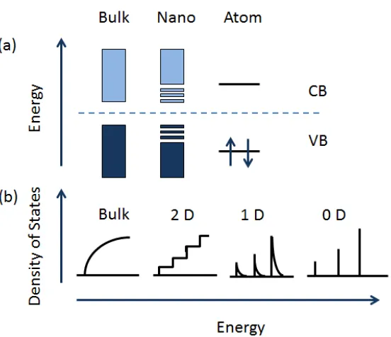
Figure 1-2 Schematic illustrations of density of states comparison (a) among bulk, nano and atom, and (b) among bulk and nanomaterials with specific dimensionality. CB: conduction band, VB: valence band
Due to the quantum confinement effect, TiO2 nanomaterials exhibit a wider band gap than that of its bulk counterpart, which means that more energy is needed to excite the electrons from VB into CB. Moreover, high surface area brought about by small particles size is beneficial to many TiO2-based devices, as it facilitates resction/interaction between the devices and the interacting media, which mainly occurs on the surface or at the interface and strongly depends on the surface area of the material. As a result, TiO2 nanomaterials lead to a higher potential of applications in soar cells, water splitting and so on.6-9
Generally speaking, the functional properties of TiO2 nanomaterials are influenced by a large number of factors.12
while these electrodes possess a high surface to volume ratio, the structural disorder at the contact between two crystalline particles leads to an enhanced scattering of free electron, thus reducing the electron mobility13. However, TiO2 NW and NT offer a large internal surface area without a concomitant decrease in geometric and structural order, which can provide direct channels for charge and mass transport to the back contact. Especially for highly ordered nanotubes arrays, it can eliminate randomization of the grain network and increases contact points for good electrical connection. Charge carrier recombination has been demonstrated to be significantly lower in dye-sensitized TiO2 nanowires and nanotubes based solar cells14-16
. Besides, for highly ordered nanotubes arrays, the porosity of the ordered structure allows the incident photons to be more effectively absorbed than on a flat electrode17
, with anisotropic optical scattering occurring when the pore
displacement period and the light wavelength have comparable values18. This thesis only focuses on the TiO2 NT and TiO2 NW.
1.1.3 Applications
All the specific properties of nanomaterials have led to the exploitation of TiO2 nanomaterials for a wide variety of applications in which TiO2 nanomaterials is essentially preferred over conventional TiO2 materials.6-9 Amongst the multiple uses of TiO2 nanomaterials, two major applications can be highlighted, photocatalytic water splitting and solar cells.
Photocatalytic water splitting
Hydrogen has been identified as a potential energy carrier due to its high energy capacity and environmental friendliness19. There are a lot of materials that can be the potential sources of hydrogen20-25. However, CO2 is produced26-28 or energy from an external resource is required29 in process of the hydrogen generation by using some of these hydrogen-containing materials. In the pursuit of a friendly way of hydrogen generation, TiO2 came onto the stage and began to show its excellent advantages. In 1972, Fujishima and Honda5 achieved water splitting using TiO2. In their pioneering work, when the
attributed to the unique electronic properties of TiO2: wide bandgap semiconductors with suitable band-edge positions and a good match of the redox potential of water. When TiO2 absorbs a photon that has energy equal or higher than energy of its band gap, electron at cole level will be excited into CB, leaving a hole at the VB. The electrons (in CB) and holes (in VB) then migrate to the surface of the photocatalyst. The eletrons then act as reducing agent and the holes act as the oxidizing agent. For instance, considering the band gap energy of TiO2 (~3.2 eV) is larger than the energy of water splitting (1.23 eV), water can be splitted into O2 and H2.
TiO2 has two major problems in the way of continuing exploitation of its functional properties. The first problem is that electrons in the VB can not be excited into conduction band by a visible light photon and TiO2 cannot take advantage of most of the sunlight spectrum on its own. In addition, once the electron-hole pairs are generated,
there are several possibilities: 1) radiative recombination of electrons and holes on the surface or in the bulk of the semiconductor; 2) non-radiative recombination of the electrons and holes; 3) electrons and holes are separated and intiate photocatalysis. So the second problem is the efficiency of the usage of solar energy is very limited. Amongst them, luminescence (radiative recombination) is one of important properties of semiconductors, which associated with near-band-gap recombination and defets. So understanding of the mechanism of the luminescence of TiO2 can help us to further improve the effeciency of the photocatalysis.
Dye-sensitized solar cells (DSSC)
DSSCs are based on dye-sensitization of a wide band gap semiconductor.30 In TiO2-based DSSC, TiO2 nanomaterials are covered with an organo-metallic dye immersed in an electrolyte containing a redox couple. The anode is composed of semiconductor with a transparent conducting electrode. The cathode is generally made of platinum or carbon. In TiO2-based DSSC, the light absorption and the charge separation functions are
rapidly reduced by electrolyte, thus preventing recombination of the electrons and holes. Electrons travel through the semiconductor to the electrode, the external load and finally to the counter electrode where they reduce the electrolyite.31 The TiO2 are important not only because of the large amount of dye that can be adsorbed on the very large surface but also for another two reasons: (a) they allow the semiconductor small prticles to become almost totally depleted upon immersion in the electrolyte (allowing for large photovoltages) and (b) the proximity of the electrolyte to all particles makes screening of injected electrons, and thus their transport, possible.32
1.1.4 Synthesis methods of TiO
2NT and NW
The growth of 1D TiO2 nanomaterials requires the arrangement of atoms in a controlled manner: e.g. composition, size growth direction and crystallinity. Various techniques have been developed to synthesize nanomaterials of desired morphologies and chemical compositions. Here, two different methods are introduced for synthesis of TiO2 NT and TiO2 NW, respectively.
Electrochemical anodization method
Highly ordered TiO2 NT arrays in this work are synthesized by electrochemical anodization. Apart from electrochemical anodization, TiO2 NT can be produced by a number of other methods. These methods include: using a template of nanoporous alumina33-36, sol-gel transcription processes using organo-gelator37,38, seeded growth mechanisms39
, and hydrothermal techniques40-42
. However, none of these methods can offer good control over the nanotube dimensions. TiO2 NT obtained is either single tubes or loose agglomerates of the tubes or bundles that are dispersed in solution. The tube lengths are also in a wide distribution. In order to make use of the structures in electrically contacted devices, the nanotubes are usually compacted into layers and attached onto electrode surface. The electrochemical anodization method is a self-organization process: arrays of oxide nanotubes are formed by etching the metal substrate. As a result, nanotubes are aligned perpendicular to the metal surface with well-defined
provide a dense and defined nanotube layer on any shape of titanium surfaces and is thus an extremely versatile parallel structuring process. The samples used in Chapter 4 are the TiO2 NT peeled off the Ti substrate.
Hydrothermal method
TiO2 NW investigated in this thesis is synthesized by hydrothermal method, which is one of the template-free methods. In the template-based methods, growth of nanowires is controlled by the template. Their growth depends on the boundary between the template and bulk liquid, which only occupies a small part of the total volume. However, the
nanowire synthesis by using template-free methods, such as hydrothermal method, require stringent growth conditions since favourable conditions are needed to promote 1D growth in the entire bulk liquid.
Hydrothermal synthesis involves the crystallization and growth of a material in the high-temperature aqueous solution at high pressures. Hydrothermal synthesis is normally conducted in reactor chamber called autoclaves with or without Teflon liners, which can provide high temperature and high pressure inside. The temperature can be increased over the boiling point of water and reach the pressure of vapour saturation. Internal pressure produced is largely determined by the temperature and the amount of solution added to the autoclave.
The starting material composition and its homogeneity, purity, and quality must be carefully controlled in hydrothermal synthesis of nanowires. Reaction temperature, pH of the solution, and the type of oxidants used are the variables which affect the product. The disadvantage of hydrothermal method is the requirement of high temperatures and pressures and the expensive reactor chamber. The growth mechanism of 1D growth is not
clearly understood yet. After the fundamental work of synthesis of TiO2 NT by Kasuga et
al40,43, the hydrothermal method is reported to be the most powerful technique because of
its simplicity and the fact that the nanowires are synthesized in cost-effective and environmentally friendly way44. Hydrothermal method has already been applied to
1.2 X-ray absorption and related spectroscopy
1.2.1 X-ray absorption near-edge structures (XANES)
When light interacts with matters, it can be totally or partially absorbed. However,
depending on the nature and the thickness of the matter, light can be totally or partially absorbed. The amount of light transmitted can be related to the intensity of incident light according to Beer’s law:
I = I0e–μt (1.1)
where I0 and I are the intensity of the incident and transmitted light, respectively, t is the sample thickness, μ is so-called absorption coefficient, as shown in Figure 1-3. For X-ray, as for all light, the X-ray intensity is proportional to the number of X-ray photons (~ 500 eV to 500 keV).
Figure 1-3 Light absorption measurements: an incident beam of intensity I0 passes
through a sample of thickness t, and the transmitted beam has intensity I.
X-ray is absorbed by all matter through the photo-electric effect. When the X-ray has
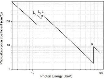
which correspond to the core electrons at different levels being excited. The edges labeled with K, L1, L2 and L3 refer to the excitations of the 1s core electrons, 2s core electrons, 2p1/2 electrons and 2p3/2 electrons, respectively. As the X-ray energy increases above the threshold, the excitation will probe the unoccupied electronic states with higher energy showing modulation in the absorption coefficient. The modulation is caused by the outgoing electron being scattered by a neighbouring atom, the feature of which is determined by the local environment (nearest neighbours and the local symmetry) of the absorbing atom.
Figure 1-4 Log-log plot of the mass absorption coefficient of platinum as a function of X-ray photo energy. 45
X-ray absorption fine structure (XAFS) hence refers to the variation of μ as a function of X-ray energy (E) of an atom in a certain chemical environment. The XAFS is typically divided into two regimes: X-ray near-edge spectroscopy (XANES) and extended X-ray absorption fine structure (EXAFS). Although the two have the same physical origin, they
or so above the edge is often referred to as the XANES. Technically, by scanning the energy from a few eV below the absorption edge up to about 50 eV above the edge, XANES records the variation of absorption coefficient as a function of energy. XANES arises from bound-to-bound (e.g. 1s to LUMO of p character), bound-to-quasibound (multiple-scattering state) and bound to continuum dipole transitions. XANES is sensitive to formal oxidation state and coordination environment and is often used to study local structure and bonding of the absorbing atom in a chemical environment.
1.2.2 X-ray excited optical luminescence (XEOL)
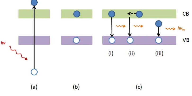
X-ray excited optical luminescence (XEOL) is an X-ray photon-in, optical photon-out spectroscopic technique that monitors light emission from matter in the optical region upon the absorption of X-ray. Figure 1-5 shows the absorption and luminescence process responsible for XEOL in a semiconductor.
The absorption of an X-ray photon creates a core hole followed by a cascade process of filling the hole with electrons from shallower levels via Auger electrons and X-ray fluorescence. In a semiconductor, the electrons and holes thermalize at the bottom of the CB and the top of VB, respectively. Then they can form an electron-hole pair (exciton) which recombines and the energy is released either radiatively (optical photon) or non-radiatively (phonon). The radiative recombination of electrons and holes will produce optical luminescence. And this process is called X-ray excited optical luminescence (XEOL). The XEOL process is shown in the Figure 1-5. The recombination can be a direct one, i.e. by the formation of an exciton. And the emitted light has energy equal to the energy difference between the band gap and the exciton binding energy. The recombination can also be an indirect one. This kind of luminescence is related to defects
such as the trapped holes, trapped electrons and impurities and thus the energy of luminescence is lower than the band gap luminescence.
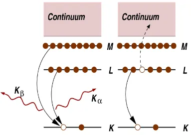
1.2.3 De-excitation processes following the X-ray absorption
Following an absorption event, the atom is said to be in an excited state, with one of the
core electron levels left empty (a so-called core hole), and a photo-electron. The excited state will eventually decay typically within a few femtoseconds after the X-ray absorption. There are two main de-excitation processes occurring to fill the core-hole. The first of the de-excitation process is X-ray fluorescence (Figure 1-6).48 The fluorescence energies emitted are element-specific, and can be used to identify the elements in a system, and to quantify their concentrations. For example, an L shell electron dropping into the K level gives the Kαfluorescence line. The second process for de-excitation of the core hole is the Auger Effect. In the Auger process, an electron at shallower level fills the core hole, and the energy released is transferred to excite another electron into continuum.
Both the Auger yield and fluorescence yield are proportional to the absorption coefficient
μ, because they are related to the probability of the presence of the core-hole created by
X-ray absorption.
XAFS can be measured by transmission or fluorescence geometries. We can measure the energy dependence of the absorption coefficient μ(E) either in transmission as
μ(E) = log (I0/I) (1.2)
or in X-ray fluorescence (or Auger emission) as
μ(E) ∝ If / I (1.3)
where If is the monitored intensity of a fluorescence line associated with the absorption process.
1.3 High pressure phenomena
1.3.1 High-pressure study
Pressure is a thermodynamic parameter of paramount importance for chemical
equilibrium and chemical kinetics. In universe, pressure spans over 60 orders of magnitude, from 10-32 Pa in the intergalactic space to 1032 Pa (1 GPa = 109 Pa) at the center of the neutron star. In such a large range of pressure, materials could have various structures with different properties. Pressure has been used to study the response of chemical systems in varying thermodynamic states in the laboratory. However, in the most of these researches, pressures applied only cover a small fraction, such as one atmosphere to a kilobar (0.1 GPa) under which “high pressure” chemical reactions are carried out. It is obvious that these so-called “high pressures” are far from the magnitude of the high pressure in our nature, such as the pressure of the earth core (around 330-360 GPa).
High-pressure studies had a real development in the past few decades and became showing its potential in the fundamental chemical studies. Modern high pressure
modern laboratories. The most popular high pressure device nowadays is the DAC which was designed by Lawson and Tang 49 and developed by Jamieson et al.50 and Weir et al.51 This kind of DAC now enable physics and chemistry experiments to be carried out in the laboratory into multimegabar range (P > 100 GPa) and the highest pressure attained in the laboratory with a DAC is around 400 GPa.52
Pressures now provided in laboratories can induce changes of free energy of materials 53 that exceed the enthalpy of those strongest chemical bonds (>10 eV). This is because pressure (P) and energy (E) has a relationship given by,
V E P
4 . 1
In the equation above, E varies with the change of the volume (V). Under high pressure, interatomic distance is significantly shortened and the system becomes thermodynamically unstable. System will eventually retrieve a new free energy minimum and be stable again. Meanwhile, systems may go through different processes, such as phase transformation, ionization, polymerization, amorphization, dissociation and, even atomization and metallization. Thus high pressure can offer enhanced opportunities to discover new phases, trigger chemical reactions, forcing materials into new physical and chemical states. For example, under high pressure, oligomerization of butadiene can achieve polymerization without catalyst at 0.7 GPa 54. Under high pressure greater than 120 GPa and temperature of 2000 K, N2 which contains the strongest homonuclear bond forms a polymer.53 Some materials can become metal under high pressure. Iodine becomes a monatomic metal by around 20 GPa. Si transforms into metallic polymorphs by 10-12 GPa.55 Once megabar pressures are attained, elements such as oxygen sulphur and xenon all become metals.56-58
Investigation of pressure-induced phase transitions and structural changes, as well as characterization of new structures in materials represents a frontier area of materials
fundamental materials for lithium battery. However, among all the polymorphs of TiO2, TiO2-B phase exhibits a higher efficiency than the rutile phase and anatase phase.62 So searching the structures with properties which can satisfy the applications is of particular interest. One approach to obtain new structures is the application of high pressure.
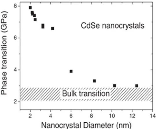
Figure 1-7 Phase transitions of wurtzite CdSe nanocrystals towards rocksalt structure as a function of the diameter of the crystal. The phase transition is taken at the midpoint of the hysteresis loop. 65, 66
1.3.2 High pressure effects on nanomaterials
The properties of nanomaterials largely depend on the synthetic methods. It has been demonstrated that high pressure can provide an additional force to modify the structures and morphologies of nanomaterials. For example, carbon nanotubes can transform into single crystal diamond at high pressure.63 Moreover, high-pressure behaviours of nanomaterials are much different from that of the corresponding bulk counterparts. For example, it is found that upon compression the bulk ZnS undergoes a phase transformation from wurtzite phase to sphalerite phase and then to rock salt phase.
directly transforms into rock salt phase and the mediate phase of sphalerite phase is bypassed.64
In addition, size of the nanomaterials is also an important factor which influences the high-pressure behaviours. For instance, CdSe nanomaterials undergo a phase transformation sequence upon compression: wurtzite phase to rocksalt phase. Interestingly, the phase transformation pressure shows a function of the size of the CdSe nanoparticles. As we can see in the Figure 1-8, with the increasing of the size of the CdSe nanoparticles, phase transformation pressure decreases. When the size of the
nanocrystalline CdSe reaches 10 nm, the transition pressure is the same as that of the corresponding bulk materials. 65,66
Although many high-pressure studies have been carried out on nanomaterials, most of them are nanoparticles. High-pressure studies on 1D nanomaterials attract much attention in recent years, not only because of their superior properties and wide applications, but also because of the morphology-effects on high-pressure behaviours which is lack of understanding.
1.4 Motivations
The chemical and physical properties of TiO2 have been widely studied since it has found
understand the basic properties of nanostructured TiO2. Optical properties of non-doped TiO2 in different crystal phases and morphologies even using different synthesis methods, which are closely related to the photocatalysis application, are not yet fully understood. Previous PL spectroscopy studies reveal that anatase TiO2 nanoparticles and TiO2 nanotubes emit visible green light and rutile TiO2 exhibit a near IR.74-76 However, considering TiO2 nanowires is one of important 1D nanomaterials in industrial applications and their electronic structures and optical properties has never been fully studied before. So in my project, TiO2 nanowires are studied by using XANES and XEOL in Chapter 3.
Compared to other nanostructure materials, one dimensional semiconducting nanomaterials have recently attracted considerable interest for their potential as the building blocks for fabricating various nanodevices.67-70 Among these semiconducting
nanomaterials, TiO2 nanotubes synthesized using electrochemical anodization exhibit better electrical properties combined with much higher specific surface areas, thus TiO2 nanotubes-based DSSC and water splitting system demonstrate far better properties.16,17 Usually, these excellent properties originate from their unique nanotubes structures and crystal structures. Therefore, it is very important to explore the properties, stabilities, compressibilities of TiO2 nanotubes under high pressure. A lot of high pressure studies of TiO2 nanomaterials have been done in recent years.77-82 Size- and morphology-effects on high-pressure behaviours of TiO2 nanomaterials are found under high pressure. As no high-pressure study on TiO2 nanotubes has been undertaken, many outstanding issues, such as, phase transition sequence, high pressure phases, compressibility, etc., still remain to be addressed. As a result, in-situ Raman spectroscopy and X-ray diffraction high-pressure study of TiO2 nanotubes is done in Chapter 4.
1.5 References
(1) Reck, E.; Richards, M. Surf. Coat. Int. Part B: Trans1977, 80, 568. (2) Pfaff, G.; Reynders, P. Chem. Rev.1999, 99, 1963.
(3) Braun, J. H.; Baidins, A.; Marganski, R. E. Prog. Org. Coat.1992, 20, 105. (4) Yuan, S.; Chen, W.; Hu, S. Mater. Sci. Eng.: C2005, 25, 479.
(6) Gratzel, M. Nature2001, 414, 338.
(7) Hagfeldt, A.; Gratzel, M. Chem.Rev.1995, 95, 49.
(8) Linsebigler, A. L.; Lu, G. Q.; Yates, J. T. Chem. Rev.1995, 95, 735. (9) Mills, A.; Le Hunte, S. J. Photochem. Photobiol. A: Chem.1997, 108, 1. (10) San-Miguel, A. Chem. Soc. Rev. 2006, 35, 876.
(11) Harris, C. I.; Savage, S.; Konstantinov, A.; Bakowski, M.; Ericsson, P. Appl. Surf. Sci.2001, 184, 393.
(12) Pavasupree, S.; Jitputti, J.; Ngamsinlapasathian, S.; Yoshikawa, S. Mater. Res. Bull.2008, 43, 149.
(13) de Jongh, P. E.; Vanmaekelbergh, D. Phys. Rev. Lett.1996, 77, 3427. (14) Zhu, K.; Neale, N. R.; Miedaner, A.; Frank, A. J. Nano Lett.2007, 7, 69.
(15) Mor, G. K.; Shankar, K.; Paulose, M.; Varghese, O. K.; Grimes, C. A. Nano Lett.
2006, 6, 215.
(16) Shankar, K.; Bandara, J.; Paulose, M.; Wietasch, H.; Varghese, O. K.; Mor, G. K.; LaTempa, T. J.; Thelakkat, M.; Grimes, C. A. Nano Lett.2008, 8, 1654.
(17) Marin, F. I.; Hamstra, M. A.; Vanmaekelbergh, D. J. Electrochem. Soc. 1996,
143, 1137.
(18) Lutich, A. A.; Gaponenko, S. V.; Gaponenko, N. V.; Molchan, I. S.; Sokol, V. A.; Parkhutik, V. Nano Lett.2004, 4, 1755.
(19) Muradov, N. Z.; Veziroglu, T. N. Int. J. Hydrogen Energ. 2008, 33, 6804. (20) Coughlin, R. W.; Farooque, M. Nature1979, 279, 301.
(21) Wang, D.; Czernik, S.; Montane, D.; Mann, M.; Chornet, E. Ind. Eng. Chem. Res.
1997, 36, 1507.
(22) Sato, S.; Lin, S. Y.; Suzuki, Y.; Hatano, H. Fuel2003, 82, 561. (23) Cortright, R. D.; Davda, R. R.; Dumesic, J. A. Nature2002, 418, 964.
(24) Lu, Y. J.; Guo, L. J.; Ji, C. M.; Zhang, X. M.; Hao, X. H.; Yan, Q. H. Int. J. Hydrogen Energ.2006, 31, 822.
(25) Hao, X. H.; Guo, L. J.; Mao, X.; Zhang, X. M.; Chen, X. J. Int. J. Hydrogen Energ.2003, 28, 55.
(26) Damen, K.; van Troost, M.; Faaij, A.; Turkenburg, W. Prog. Energ. Combust.
(27) Cormos, C.-C.; Starr, F.; Tzimas, E.; Peteves, S. Int. J. Hydrogen Energ. 2008,
33, 1286.
(28) Cobden, P. D.; van Beurden, P.; Reijers, H. T. J.; Elzinga, G. D.; Kluiters, S. C. A.; Dijkstra, J. W.; Jansen, D.; van den Brink, R. W. Int. J. Greenhouse Gas Control2007, 1, 170.
(29) Wang, Y.; Li, H.; He, P.; Zhou, H. Chemsuschem 2010, 3, 571.
(30) Grätzel, M. J. Photochem. Photobiol. C: Photochem. Rev.2003, 4, 145. (31) O'Regan, B.; Gratzel, M. Nature1991, 353, 737.
(32) Cahen, D.; Hodes, G.; Grätzel, M.; Guillemoles, J. F.; Riess, I. J. Phys. Chem. B
2000, 104, 2053.
(33) Lakshmi, B. B.; Dorhout, P. K.; Martin, C. R. Chem. Mater.1997, 9, 857. (34) Hoyer, P. Langmuir1996, 12, 1411.
(35) Imai, H.; Takei, Y.; Shimizu, K.; Matsuda, M.; Hirashima, H. J. Mater. Chem.
1999, 9, 2971.
(36) Michailowski, A.; AlMawlawi, D.; Cheng, G.; Moskovits, M. Chem. Phys. Lett.
2001, 349, 1.
(37) Jung, J. H.; Kobayashi, H.; van Bommel, K. J. C.; Shinkai, S.; Shimizu, T. Chem. Mater.2002, 14, 1445.
(38) Kobayashi, S.; Hamasaki, N.; Suzuki, M.; Kimura, M.; Shirai, H.; Hanabusa, K.
J. Am. Chem. Soc. 2002, 124, 6550.
(39) Tian, Z. R.; Voigt, J. A.; Liu, J.; McKenzie, B.; Xu, H. J. Am. Chem. Soc.2003,
125, 12384.
(40) Kasuga, T.; Hiramatsu, M.; Hoson, A.; Sekino, T.; Niihara, K. Langmuir 1998,
14, 3160.
(41) Chen, Q.; Zhou, W.; Du, G. H.; Peng, L. M. Adv. Mater.2002, 14, 1208.
(42) Yao, B. D.; Chan, Y. F.; Zhang, X. Y.; Zhang, W. F.; Yang, Z. Y.; Wang, N.
Appl. Phys. Lett.2003, 82, 281.
(43) Kasuga, T.; Hiramatsu, M.; Hoson, A.; Sekino, T.; Niihara, K. Adv. Mater.1999,
11, 1307.
(45) Website: http://physics.nist.gov/PhysRefData/FFast.
(46) Sham, T. K.; Jiang, D. T.; Coulthard, I.; Lorimer, J. W.; Feng, X. H.; Tan, K. H.; Frigo, S. P.; Rosenberg, R. A.; Houghton, D. C.; Bryskiewicz, B. Nature 1993,
363, 331.
(47) Sham, T. K.; Naftel, S. J.; Kim, P. S. G.; Sammynaiken, R.; Tang, Y. H.; Coulthard, I.; Moewes, A.; Freeland, J. W.; Hu, Y. F.; Lee, S. T. Phys. Rev. B
2004, 70, 405313.
(48) Newville, M.; Consortium for Advanced Radiation Sources: Chicago, 2004. (49) Lawson, A. W.; Tang, T. Y. Rev. Sci. Instrum.1950, 21, 815.
(50) Jamieson, J. C.; Lawson, A. W.; Nachtrieb, N. D. Rev. Sci. Instrum. 1959, 30, 1016.
(51) Weir, C. E.; Lippincott, E. R.; Vanvalkenburg, A.; Bunting, E. N. J. Res. NBS A Phys. Chem.1959, 63, 55.
(52) Ruoff, A. L.; Xia, H.; Luo, H.; Vohra, Y. K. Rev. Sci. Instrum.1990, 61, 3830. (53) Hemley, R. J. Annu.Rev. Phys.Chem.2000, 51, 763.
(54) Citroni, M.; Ceppatelli, M.; Bini, R.; Schettino, V. Science2002, 295, 2058. (55) Bassett, L.-G. L. a. W. A. Elecments, Oxides, Silicates: High-Pressure Phases
with Implications for the Earth's Interior; Oxford University Press: New York, 1986.
(56) Eremets, M. I.; Gregoryanz, E. A.; Struzhkin, V. V.; Mao, H. K.; Hemley, R. J.; Mulders, N.; Zimmerman, N. M. Phys. Rev. Lett.2000, 85, 2797.
(57) Struzhkin, V. V.; Hemley, R. J.; Mao, H. K.; Timofeev, Y. A. Nature1997, 390, 382.
(58) Amaya, K.; Shimizu, K.; Eremets, M. I. Int. J. Mod. Phys. B1999, 13, 3623. (59) Watson, J.; Ihokura, K.; Coles, G. S. V. Meas. Sci. Tech. 1993, 4, 711. (60) Wang, X.; Song, J.; Liu, J.; Wang, Z. L. Science2007, 316, 102.
(61) Liu, Y.; Yang, Q.; Zhang, Y.; Yang, Z.; Wang, Z. L. Adv. Mater.2012, 24, 1410. (62) Armstrong, G.; Armstrong, A. R.; Canales, J.; Bruce, P. G. Electrochem. Solid St.
(63) Blank, V. D.; Denisov, V. N.; Kirichenko, A. N.; Lvova, N. A.; Martyushov, S. Y.; Mavrin, B. N.; Popova, D. M.; Popov, M. Y.; Tat’yanin, E. V.; Zakhidov, A. A. Phys. B.2006, 382, 58.
(64) Wu, C.; Feng, F.; Feng, J.; Dai, J.; Yang, J.; Xie, Y. J. Phys. Chem. C2011, 115, 791.
(65) Tolbert, S. H.; Alivisatos, A. P. J. Chem. Phys.1995, 102, 4642.
(66) Jacobs, K.; Zaziski, D.; Scher, E. C.; Herhold, A. B.; Alivisatos, A. P. Science
2001, 293, 1803.
(67) Liu, B.; Nakata, K.; Liu, S.; Sakai, M.; Ochiai, T.; Murakami, T.; Takagi, K.; Fujishima, A. J. Phys. Chem. C2012, 116, 7471.
(68) Tokudome, H.; Miyauchi, M. Chem. Commun. 2004, 958.
(69) Zhu, H. Y.; Gao, X. P.; Lan, Y.; Song, D. Y.; Xi, Y. X.; Zhao, J. C. J. Am. Chem. Soc.2004, 126, 8380.
(70) Yamabi, S.; Imai, H. Chem. Mater.2002, 14, 609.
(71) Asahi, R.; Morikawa, T.; Ohwaki, T.; Aoki, K.; Taga, Y. Science2001, 293, 269. (72) Nah, Y.-C.; Paramasivam, I.; Schmuki, P. Chemphyschem2010, 11, 2698.
(73) Bingham, S.; Daoud, W. A. J. Mater. Chem. 2011, 21, 2041.
(74) Wang, X.; Feng, Z.; Shi, J.; Jia, G.; Shen, S.; Zhou, J.; Li, C. Phys. Chem. Chem. Phys.2010, 12, 7083.
(75) Knorr, F. J.; Mercado, C. C.; McHale, J. L. J. Phys. Chem. C2008, 112, 12786. (76) Shi, J.; Chen, J.; Feng, Z.; Chen, T.; Lian, Y.; Wang, X.; Li, C. J. Phys. Chem. C
2007, 111, 693.
(77) Li, Q.; Liu, B.; Wang, L.; Li, D.; Liu, R.; Zou, B.; Cui, T.; Zou, G.; Meng, Y.; Mao, H.-k.; Liu, Z.; Liu, J.; Li, J. J. Phys. Chem. Lett.2010, 1, 309.
(78) Li, Q.; Cheng, B.; Yang, X.; Liu, R.; Liu, B.; Liu, J.; Chen, Z.; Zou, B.; Cui, T.; Liu, B. J. Phys. Chem. C2013, 117, 8516.
(79) Dong, Z., University of Western Ontario, 2012.
(81) Swamy, V.; Dubrovinsky, L. S.; Dubrovinskaia, N. A.; Langenhorst, F.; Simionovici, A. S.; Drakopoulos, M.; Dmitriev, V.; Weber, H. P. Solid State Commun.2005, 134, 541.
(82) Hearne, G. R.; Zhao, J.; Dawe, A. M.; Pischedda, V.; Maaza, M.; Nieuwoudt, M. K.; Kibasomba, P.; Nemraoui, O.; Comins, J. D.; Witcomb, M. J. Phys. Rev. B
Chapter 2 Instrumentation
2.1 Synchrotron radiation
2.1.1 Principle of synchrotron radiation
Synchrotron radiation is produced by accelerating electrons approaching the speed of light1. Controlled by a magnetic field, electromagnetic radiation is produced tangentially to the curved orbit of accelerated electrons. The power of the radiation by accelerated electrons is given by
3 2 P
2 4 2 0
4 2
c m
cE e
2.1
where e is the electron charge, c is the speed of light, E is the energy of electron (in GeV),
m0 is the rest mass of the electron, and ρ is the radius of the curvature.
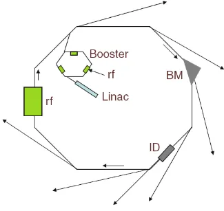
Figure 2-1 shows a schematic layout of a synchrotron radiation facility. First the generated electrons are accelerated to a speed close to the speed of light with energy of hundreds of MeV in the linear accelerator (LINAC). Then the electrons are injected into the booster ring and further accelerated to reach the 99.9999985% of the speed of light.3 Finally electrons are injected into the storage ring and circulate for several hours. The storage ring consists of straight sections and curved sections. In the curved sections bending magnets are located, which bend the electron beam and make up a 360° bending in total. In the straight sections, the wigglers and undulators, known as “insertion devices” are placed.
Synchrotron radiation is emitted while the trajectory of the accelerated electrons is altered. This is achieved by the use of two kinds of magnets, the bending magnets, and the insertion devices (wigglers and undulators). The magnetic field in the vertical direction of
bending magnets and insertion devices cause the oscillation of electrons in the horizontal plane. Each type of magnets provides radiation of different spatial distribution, which is determined by the opening angle (1/γ). γ is given by (Equation 1.8).
2
0c
m E
2.2As shown in Figure 2-2, considering the electron beam bend along the orbit of curved section, a bending magnet produces sharp cone of radiation in the bending plane, shown in Figure 2-3. Because wigglers have high magnetic field, radiation beam generated in
Figure 2-2 Schematic of a (a) bending magnet, (b) wiggler and (c) undulator. 5
Figure 2-3 Opening angle and flux (vs. Ephoton) of (a) bending magnets, (b) wigglers,
and (c) undulators.6
magnitude as that of the traditional X-ray; (3) the beam is highly collimated, which is able to provide a very small focal spot or highly spatial resolution.
Figure 2-4 Schematic layout of the CLS beamlines.7
2.1.2 Synchrotron facilities
Canadian Light Source (CLS)
provide photons from far IR to hard X-ray. The storage ring has a circumference of 171 m and is operated at an energy of 2.9 GeV and 500 mA.
Figure 2-5 Schematic layout of the APS beamlines8
Advanced Photon Source (APS)
Figure 2-5 shows the layout of the APS. Advanced Photon Source (APS) is located at
Argonne National Laboratory, Argonne, USA. It consists of 34 sectors, and each sector contains one or more beamlines for a variety of researches. The storage ring has a circumference of 1104 m and is operated at 7 GeV and current of 102 mA that runs in “top-up” mode, which means the beam is kept as a constant beam current by injection
2.1.3 Beamlines
High resolution spherical grating monochromator (SGM)
beamline-CLS: sector 11 insertion device-section 1 (11ID-1)
The SGM beamline in CLS is used to conduct the X-ray absorption measurements in my project. SGM beamline (11ID-1) at CLS has the energy range from 250 eV to 2000 eV, which is ideal for studying K-edges of low-Z elements and L-edges of transition metals. SGM has three gratings available: low energy grating, medium energy grating and high energy grating, which correspond to different energy ranges, 250-700 eV, 450-1250eV and 740-2000 eV respectively. The resolution E/ΔE is > 5000 at energy below 1500 eV with focal spot of 1000 μm×100 μm. Under 100 mA, SGM produce a flux (photons/s) is > 1012 at 250 eV and >1011 at 1900 eV. 9
Beamline-APS: sector 16 insertion device-section B (16 ID-B)
The 16ID-B beamline in APS is a dedicated high-pressure beamline for X-ray diffraction measurements. The source for 16ID-B is the dual undulator Type A, which provides X-ray in the energy region from 6 keV – 40 keV (normal) up to 60 keV – 70 keV. A Si double crystal was employed as monochromator. This beamline can provide a beam size of 4×5 μm2 with the help of 200 mm KBr mirrors and produce a flux of 5 × 10¹⁰ photons/s at the sample position. Such a small beam size and high energy at the sample position make it possible to conduct the XRD measurement on different sample spots in relatively short accumulation time. Besides, a MAR345 imaging plate detector is used to collect the diffraction patterns of the sample. In addition to the XRD technique, 16ID-B also provides many excellent technical supports such as the membrane and mechanical pressure control, online ruby and Raman system, and offline alignments and Ruby system.
2.2 High pressure techniques
Figure 2-6 (a): Side view of an assembled symmetric piston-cylinder type DAC and (b): photo of the dissemble DAC with two parts, piston (right hand) and cylinder (left hand). 2
Figure 2-7 The schematics of a DAC (a) and enlarged view (b) of the red square area in (a).2
There are two reasons to use the diamond as anvil. First, the diamond is the hardest material in nature. Therefore, diamond can sustained very high pressure on samples without breaking itself. Second, diamond is transparent to a wide range of electromagnetic radiation. As a result, the structure of the materials at high pressure can be characterized by multi techniques such as Raman and IR spectroscopy, XRD etc. There are two different types of diamonds used in DAC. Type I diamonds with higher impurity (e.g. nitrogen) are used for Raman and XRD measurement. Type II diamonds are used for IR measurements.
2.2.2 The ruby pressure gauge
For all high pressure experiments, reliable and accurate pressure gauge is very important. In our laboratory, a ruby gauge is adopted for the in situ high-pressure calibration in DAC, which is established by Mao. 10 Ruby is Al2O3 doped with Cr3+. It has two dominant
and R2 transitions involving the Cr3+ ion. These two peaks are very sensitive to pressure and the peak positions shift to longer wavelength upon compression. As a result, the relationship between pressure and peak shift can be used to measure the pressure of the sample.
Figure 2-8 Ruby fluorescence measured at different pressures with the two luminescent peaks labeled (R1 and R2).2
The equation shown below is used to determine the pressure by measuring ruby fluorescence spectra.
1
24 . 694 1
1904 B
B
P
2.3where P represents pressure in GPa, Δλ represents the shift of the R1 peak. The parameter B is equal to 7.665 for quasi-hydrostatic conditions, and is equal to 5 for non-hydrostatic
conditions. An example is shown in Figure 2-8. With the pressure increasing from 0.2 GPa to 0.8 GPa, there is a 0.25 red shift in R1 peak.
In high pressure range, homogeneity becomes a very serious problem. And the pressure across the sample chamber may not be uniform. So in order to improve the hydrostatic conditions, a pressure transmitting medium (PTM) is also loaded into the sample chamber. There several different kinds of PTM, which can maintain the hydrostatic condition up to different pressure. The first kind of PTM includes such as alcohol mixtures made of 4:1 methanol-ethanol and 16:3:1 methanol-ethanol-H2O. This kind of PTM can maintain the hydrostatic condition to about 10.5 GPa.11-13The second kind of PTM can achieve higher pressure with keeping hydrostatic condition, such as silicon oil. Although silicon oil is much better than the alcohol mixtures, it cannot maintain the hydrostatic condition above 20 GPa.14 This is because at about 20 GPa silicon oil undergoes a glass phase transition and lose its pressure transmitting ability. So if we want reach the pressure above 20 GPa
or even higher pressure, the third PTM, noble gases, need to be introduced. Noble gases, such as Ne, Ar and He, are the best hydrostatic PTM known so far.14 Ne, for example, can maintain the hydrostatic condition as high as 50 GPa. So the PTM used in the experiments varies as the highest pressure needed to be reached.
2.3 Raman spectroscopy
Due to diamond being transparent to a wide range of electromagnetic waves, different types of radiations can be used to characterize samples in DAC under high pressure.
scattering. However, only Stokes lines are measured in most instruments, because they are more intense than the anti-stokes lines. The energy difference between the incident and scattering photons is call Raman shifts, which can provides valuable spectroscopic information for the vibrational or rotational energy of the sample. Raman Scattering mechanism is shown in Figure 2-9.
Figure 2-9 Three types of Raman scattering: Rayleigh Scattering, Stokes Raman Scattering and Anti-Stokes Raman Scattering.2
Figure 2-10 Raman system in the Song Lab: photo of the customized Raman system.
Besides, spectrometer is equipped with a triple grating (300 g/mm, 1200 g/mm, and 1800
g/mm) system with different resolutions. Standard neon lines are used to calibrate the system. With the calibration, the Raman system could achieve an uncertainty of ±1 cm-1.
2.4 Other characterization techniques
2.4.1 Powder X-ray diffraction
The conventional powder X-ray diffraction facility in Department of Earth Science is also used to check the phase of the products at ambient condition. The X-ray diffraction facility is equipped with a Rigaku X-ray diffractometer and a Co K- radiation X-ray source.
2.4.2 Scanning electron microscope (SEM)
SEM images were collected by using the Leo-Zesis 1530 SEM from Western
2.5. References
(1) Doniach, H. W. a. S. Synchrotron Radiation Research; Plenum Press: New York, 1980.
(2) Dong, Z., The University of Western Ontario, 2008.
(3) Walker, T. Introduction to Synchrotron Radiation; Canadian Light Source.
(4) Winich, H. In Synchrotron Radiation Sources: a primer; Winick, H ed.; World Science: 1994; Vol. 1.
(5) Adapted from
http://internal.physics.uwa.edu.au/~hammond/SyncRes/making-synchrotron-light.htm.
(6) Adapted from Intro to Synchrotron Radiation, D. Atwood 16th Jan 2007
http://ast.coe.berkeley.edy/srms/2007/Intro2007.pdf.
(7) Picture Courtesy of the Canadian Light Source.
http://www.lightshource.ca/experimental/images/CLS_Experimental_Hall_2011.p
ng.
(8) Picture Courtesy of the Advanced Photon Source.
http://www.aps.anl.gov/Beamlines/Images/planview_11_3_11.jpg.
(9) Regier, T.; Krochak, J.; Sham, T. K.; Hu, Y. F.; Thompson, J.; Blyth, R. I. R.
Nucl. Instrum. Methods Phys. Res. Sec. A 2007, 582, 93.
(10) Mao, H. K.; Xu, J.; Bell, P. M. J. Geophys. Res-Solid 1986, 91, 4673. (11) Marshall, W. G.; Francis, D. J. J. Appl. Crystallogr.2002, 35, 122.
(12) Angel, R. J.; Bujak, M.; Zhao, J.; Gatta, G. D.; Jacobsen, S. D. J. Appl. Crystallogr.2007, 40, 26.
(13) Klotz, S.; Strassle, T.; Rousse, G.; Hamel, G.; Pomjakushin, V. Appl. Phys. Lett.
2005, 86, 031917.
(14) Klotz, S.; Chervin, J. C.; Munsch, P.; Le Marchand, G. J. Phys. D-Appl. Phys.
2009, 42, 075413.
Chapter 3 XANES and XEOL studies of TiO
2nanowires
3.1 Introduction
Nanostructured TiO2 is of great interest for possible application in photovoltaic cells, semiconductor photo-catalyst support, and gas and humidity sensor.1-9 Insights gained
from the electronic structure of TiO2 NW will improve the understanding of this material, which will facilitate its engineering design. It is crucial to evaluate the structure and electronic properties of TiO2 NW so that the optimal structures for specific applications can be realized and one can then increase the efficiencies for solar cells, electrolysis, and
photocatalysis. XANES is a spectroscopic technique, which can probe the local symmetry and occupation of the states. The Ti L3,2-edge of TiO2 probes electron transition from Ti 2p to the conduction band of Ti 3d character, and the O K-edge probes the O 1s to 2p
transition. The spectral features thus provide the information of the unoccupied density of states. Amorphous and crystalline TiO2 differ in d-orbital splitting due to different degrees of distortion of the Ti-O octahedron and long-range order. So XANES, which measures the modulation of the X-ray absorption coefficient across an absorption threshold of the element of interest in a chemical environment, is a powerful tool in studying electronic structure.
Photoluminescence is a non-destructive and high-sensitivity technique widely used to investigate the photophysical and photochemical properties of solid semiconductors. The investigation of TiO2 by PL can give us a better understanding about the optical properties of TiO2. It is well known that the photoactivity of TiO2 heavily depends on its crystal structure,10,11 surface properties,12,13 etc., which have essential correlation with the
luminescence feature of TiO2. Therefore, the investigation of TiO2 by PL spectroscopy can provide information about the surface structure of TiO2 and their contributions to the photoreaction performance of TiO2.14,15 Since most of the luminescence studies were carried out using a fixed excitation energy from a UV-visible source, the observed
XANES and XEOL studies of 1D nanostructured TiO2 in Dr. T. K. Sham’s group is started by Dr. Lijia Liu. The phase transformation process of TiO2 NT induced by calcination was investigated.16 It has been found that TiO2 nanotubes synthesized by anodization undergo amorphous-anatase-rutile phase transformation with the calcination temperature increasing. TiO2 nanotubes show distinct optical properties at different crystal phases. Considering the electronic and optical properties of nanostructured TiO2 could be highly dependent on the defect, surface state, purity, and morphology, it is very interesting and necessary to look into nanostructured TiO2 of different morphologies synthesized by different methods and the corresponding electronic structures and optical properties. In this work, the TiO2 nanowires were synthesized using hydrothermal method, and their electronic structure and optical properties were studied using XANES and XEOL.
3.2 Experimental section
3.2.1 Sample preparation
TiO2 nanowires were prepared using the hydrothermal method.17,18 Anatase TiO2 nanoparticles with average size of ~ 25 nm were purchased from “Nanostructured & Amorphous Material Inc.” and used without further purification. In a typical preparation procedure, 1 g of TiO2 nanoparticle powders was placed into a Teflon-lined bottle with a capacity of 60 mL with 40 mL NaOH aqueous solution with the molarity of 10 M. Then the Teflon bottle was sealed into a stainless steel autoclave and maintained at a
temperature of 200 °C for 24 h without shaking or stirring. After the autoclave was naturally cooled to room temperature, the sample obtained was sequentially washed with diluted HCl aqueous solution (1% wt), deionized (DI) water, and anhydrous ethanol alternatively until pH = ~ 7. The after-washed samples were dried at 70 °C for 6 h in air,
3.2.2 Characterization
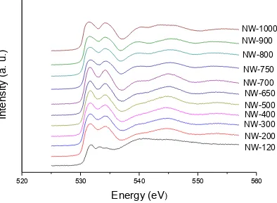
Synchrotron radiation experiments were conducted at the High Resolution SGM beamline (Energy: 250-2000 eV, ΔE/E < 2×10⁻⁴) at the CLS, University of Saskatchewan. XANES spectra were recorded in total electron yield (TEY), fluorescence yield (FLY) and photoluminescence yield (PLY, zero order). XEOL spectra, where applicable, were recorded with an optical spectrometer (Miniature Fiber Optic Spectrometer, USB65000, Ocean Optics). All spectra were normalized to the incident photon flux (I0).
The powder X-ray diffraction facility in the Department of Earth Science was used to examine the crystallinity of the as-prepared products. The X-ray diffraction facility has a Rigaku X-ray diffractometer and uses the Co K-α radiation as the X-ray source.
The morphology of TiO2 nanowires samples was characterized by Scanning Electron Microscopy (LEO 1530 SEM, LEO 1540 FIB/SEM) in the Nanofabrication Laboratory, the University of Western Ontario.
3.3 Results and discussion
3.3.1 Morphology
Figure 3-1 SEM images of (a) as-prepared nanowires and TiO2 NW calcinated for
2h (b) at 650 ℃; (c) at 700 ℃; (d) at 800 ℃; (e) at 900 ℃; (f) at 1000℃.
a)
b)
d)
e)
f)
450 460 470 480
c2 c1 b2 b1
In
te
ns
ity
(
a.u
.)
Energy (eV)
Rutile Anatase
a
Figure 3-2 Ti L3,2-edge XANES TEY of anatase phase of TiO2 (red curve) and rutile
phase of TiO2 (blue curve)
3.3.2 XANES study of calcinated TiO
2NW
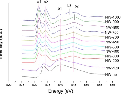
Figure 3-2 shows the Ti L3,2-edge XANES of commercial anatase and rutile. Figure 3-3 shows the Ti L3,2-edge XANES of the as-prepared nanowires and the calcinated TiO2 NW. The spectra shown in Figure 3-3 were recorded in TEY, which probe the sample surface of a few nanometers. Characteristic features of TiO2 which is observed in Figure 3-2 correspond to transitions of Ti 2p electrons to unoccupied 3d electronic states. In Figure
3-2, peaks a, b1, and b2 is attributed to L3-edge (transition of 2p3/2-3d), and peaks c1 and c2 is attributed to L2-edge (transition of 2p1/2-3d). Due to the crystal field splitting of 3d orbit distortion of Ti, both edges have two groups of peaks. By applying the molecular orbital in the case of 3d transition metal,19 a and c1 is assigned to the transition 2p-t2g and