BROADBAND STACKED U-SLOT MICROSTRIP PATCH ANTENNA
J. A. Ansari and R. B. Ram
Department of Electronics and Communication University of Allahabad
Allahabad-211002, India
Abstract—A broadband stacked U-slot microstrip patch antenna is presented using circuit theory concept. The antenna shows two resonance frequencies that are very closely spaced to give broadband characteristics. The frequency band of 186 MHz (36.4% impedance bandwidth) is achieved for the proposed antenna. The theoretical results are in good agreement with the simulated results.
1. INTRODUCTION
Microstrip antennas have become attractive candidates in a variety of commercial applications such as mobile and satellite communications. Traditionally, microstrip antennas suffer from low bandwidth characteristic. Experimentally and theoretically, it has been shown that a coaxially fed patch antenna on a foam substrate of approximately 0.08 wavelength thick can enable an impedance bandwidth of about 33%, by cutting proper U-slot in the patch [1, 2]. Moreover, Lee and Lee [3] have experimentally demonstrated the characteristics of two-layer electro-magnetically coupled rectangular patch and reported that relatively large bandwidth could be obtained when the separation between the two layers was less than 0.15 wavelength. Therefore, in the present paper, a stacked U-slot microstrip antenna is presented for broadband operation. The modal expansion cavity model and circuit theory concept have been used to analyze the antenna characteristics. The details of theoretical investigations are given in the following sections.
2. THEORETICAL CONSIDERATIONS
Wd = 30 mm and it is printed on a grounded substrate of thickness h1 = 1.59 mm and dielectric constant εr1 = 2.17. A U-slot with dimensions arm-length Ls = 16.50 mm, base-length Ws = 12.50 mm
and slot-widthS = 2.5 mm is cut in the patch in such a way that the side arms of U-slot are symmetrically positioned with respect to the feed point. The upper square patch has dimensionsLp=Wp = 18 mm that is etched on a substrate of thickness h2 = 1.59 mm and dielectric constant εr2 = 2.17. The upper parasitic patch is separated from lower fed patch by air-gap spacing (ha = 3.50 mm) introduced by a foam material of dielectric constant εra= 1.
(a) (b)
Figure 1. Geometry of the proposed antenna. (a) Top view and (b) side view.
When lower patch is coaxially fed at y0 = 6.15 mm, the upper parasitic patch is electro-magnetically, coupled to the lower fed patch through the air-gap that is realized by current distribution at frequency 4.09 GHz as shown in Figure 2.
(a) (b)
Due to presence of the parasitic patch in the stacked configuration, there are two resonances associated with the two constitutive resonators. One resonance is associated with resonator formed by the lower patch and ground plane. The second resonance is associated with the resonator formed by the upper patch and the lower patch. The effective dielectric constant of the antenna structure can be calculated as [4]
εre= h1+h2+h3
h1
εr1 + ha
εra
+ h2
εr2
(1)
The effective dielectric constant of substrate-1, can be expressed as
εed =
εre+ 1
2 +
εre−1 2
1 +10h1
Ld
−1/2
(2)
Therefore, the resonance frequency of the lower patch of the stacked antenna can be expressed [5]
f r1 =
c
2Ld√εed
1−A
1 +Aln
1.123Ld√εed h1
(3)
wherec is the velocity of light in free space, and
A= 2
πεed
Ld h1
+ 1.393 + 0.667 ln
Ld h1
+ 1.444
The resonance frequency of the upper patch can be given as
fr2=
c
2(Lp+ ∆Lp)√εep (4)
where ∆Lp is the line extension of the upper patch, and εep is the effective dielectric constant of substrate-2 that can be calculated using Equation (2) for the upper patch.
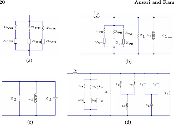
The U-slot cut in the lower patch can be considered as a combination of three narrow slots joint together in the form of U-shape. Using duality relationship of dipole and slot, the equivalent circuit of U-slot can be represented as shown in Figure 3(a). Here, RU H, XU H andRV H,XV H are radiation resistance and reactive component
(a)
(c) (d)
(b)
Figure 3. Equivalent circuits of (a) U-slot. (b) Lower patch with u-slot. (c) Upper patch and (d) proposed antenna.
and capacitance. Therefore, the equivalent circuit of the lower and upper patches can be given as shown in Figure 3(b) and Figure 3(c) respectively. When a coaxial probe feeds the lower patch, the upper patch is electro-magnetically coupled to the lower patch. As a result of this coupling, two closed and distinct resonance frequencies appears in the antenna to give broadband operation. Thus the equivalent circuit of the proposed antenna can be given as shown in Figure 3(d). In the equivalent circuit shown in Figure 3(d), one can take
ZU H = RU H +jXU H (5)
ZU V = RV H+jXV H (6) R = R1R2
R1+R2
(7)
L = L1L2
L1+L2
+LM (8)
and
C= (C1+C2)CM
C1+C2+CM
(9)
capacitance of lower patch (without slot) and upper patch respectively.
LM and CM are the mutual inductance and capacitance due to
electromagnetic coupling between the two patches.
Hence the input impedance of the antenna can given as
ZIN =
1 1
ZU
+ 1
R +jωC+
1
jωL
(10)
where
ZU =
ZU V + 2ZU H
ZU VZU H (11)
The reflection coefficient (ρ) of the antenna is given as
ρ=Zin−Z0
Zin+Z0
(12)
where Z0 is the characteristic impedance of the coaxial feed line (50 ohm).
Therefore, the return loss (RL) of the antenna is given as
RL= 10 log
1
ρ2
(13)
Since for the far-field radiation, the distance between fed patch and parasitic patch is very small as compared to the far field point, therefore the radiations from the two patches can be considered in the same phase. Also the slot voltage induced in the parasitic patch is cc
times the slot voltage of the driven patch. Therefore, the radiation field for the proposed antenna for far field radiation can be written as
E(θ) =Ed(θ) +Ep(θ) (14)
and
E(φ) =Ed(φ) +Ep(φ) (15)
where the radiation fields Ed and Ep for driven and parasitic patches are given as [8]
Ed(θ) = −jk0WdV0e
−k0r
πr cos (k0h1cosθ)
sin (k0Wdsinφsinθ)
2
k0Wdsinφsinθ
2
cos
k0(Ld+ ∆Ld)
2 sinθsinφ
Ed(φ) =−
jk0WdV0e−k0r
πr cos (k0h1cosθ)
sin (k0Wdsinφsinθ)
2
k0Wdsinφsinθ
2 cos
k0(Ld+ ∆Ld)
2 sinθsinφ
cosφ (17)
Ep(θ) =−jk0WpV0e
−k0r
πr cos(k0(h1+ha)cosθ)
sin (k0Wpsinφsinθ)
2
k0Wpsinφsinθ
2 cos
k0(Lp+ ∆Lp)
2 sinθsinφ
cosθsinφ (18)
Ep(φ) =−
jk0WpV0e−k0r
πr cos(k0(h1+ha)cosθ)
sin (k0Wpsinφsinθ) 2
k0Wpsinφsinθ 2 cos
k0(Lp+ ∆Lp)
2 sinθsinφ
cosφ (19)
whereV0 is the radiating edge voltage,ris the distance of an arbitrary far-field point andk0 is the propagation constant in free space.
2 2.5 3 3.5 4 4.5 5 5.5 6
-30 -25 -20 -15 -10 -5 0 Frequency (GHz) R e tu rn L o s s (d B ) Theoretical Simulated
3. CALCULATIONS AND DISCUSSION OF RESULTS
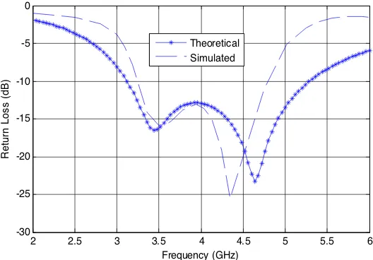
The calculations for return loss of the antenna were carried out using Equation (13); the resulting data are shown in Figure 4. It depicts the antenna has two resonance frequencies, one at 3.44 GHz and other at 4.60 GHz. These two resonance frequencies are closely spaced to give broadband characteristic. The frequency band of operation is obtained approximately equal to 186 MHz for return loss values less than 10 dB. The antenna shows an impedance bandwidth of 36.40%.
On the other hand, simulated result shows 33.89% impedance bandwidth. Thus theoretical results are in good agreement with the simulated results and therefore, the validity of the proposed method is justified.
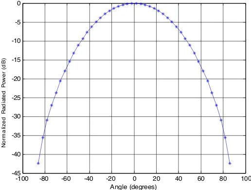
The data for E-plane radiation pattern of the proposed antenna at frequency 4.09 GHz, were calculated using Equations (14) & (15), the data so obtained are shown in Figure 5. It is observed that the 3 dB beam width of the antenna is 52.4◦.
-100 -80 -60 -40 -20 0 20 40 60 80 100
-45 -40 -35 -30 -25 -20 -15 -10 -5 0
Angle (degrees)
No
rm
a
liz
ed
R
ad
ia
ted
Po
we
r
(d
B)
Figure 5. E-plane radiation pattern.
4. CONCLUSIONS
REFERENCES
1. Huynh, T. and K. F. Lee, “Single layer single patch wideband microstrip antenna,” Electronics Letters, Vol. 31, No. 16, 1310– 1312, 1995.
2. Lee, K. F., K. M. Luk, K. F. Tong, S. M. Shum, T. Huynh, and R. Q. Lee, “Experimental and simulation studies of the co-axially fed U-slot rectangular patch antenna,”IEE Proc. Microw. Antenna Propag., Vol. 144, No. 5, 354–358, 1997.
3. Lee, R. Q. and K. F. Lee, “Experimental study of the two layer electro magnetically coupled rectangular patch antenna,” IEEE Trans. Antenna Propag., Vol. 38, No. 8, 1298–1302, 1990.
4. Liu, Z. F., P. S. Kooi, L. W. Li, M. S. Leong, and T. S. Yeo, “A method for designing broad band microstrip antennas in multilayered planar structures,” IEEE Trans. Antenna Propag., Vol. 47, No. 9, 1416–1420, 1999.
5. Pues, H. and A. Van de Capelle, “Accurate transmission line model for the rectangular microstrip antenna,”IEE Proc. - Micro. Antenna Propag., Vol. 133, Pt. H., 334–340, 1984.
6. Ansari, J. A. and R. B. Ram, “Analysis of broad band U-slot microstrip patch antenna,” Microwa. Opt. Tech. Lett., Vol. 50, No. 4, 1069–1073, 2008.
7. Bahl, J. and P. Bhartia, Microstrip Antennas, Artech House, Dedham, 1980.
8. Carver, K. R. and J. W. Mink, “Microstrip antenna technology,”