Impact of Novel Fin Shaped Structures on
Various Parameters
Daughty Abraham1, Abraham George2
PG Student [VLSI & ES], Dept. of ECE, Saintgits College of Engineering, Kottayam, Kerala, India1 Assistant Professor, Dept. of ECE, Saintgits College of Engineering, Kottayam, Kerala, India2
ABSTRACT: Beyond 22 nm technology, FinFETs have become prominent device inorder to reduce the short channel effects. Here, the effect of fin shape on threshold voltage, subthreshold swing, leakage current and Ion/Ioff ratio is
evaluated using TCAD.
The fin shape can be changed by varying the top width of the fin. There was a reduction in leakage current by 92% in the case of triangular fin when compared with rectangular fin of same base width. Here, novel fin shaped structures like concave and convex FinFETs are developed and their variations with different parameters are evaluated in these structures. Simulation results indicate that by using concave and convex fin structures, all the parameters are improved further.
KEYWORDS: FinFET, Threshold Voltage, Subthreshold Swing, Leakage
I.INTRODUCTION
For many years now, the idea of scaling leads to the shrinking of MOSFETs [6]. By scaling, large transistor is scaled down to smaller transistor with similar behaviour by a scaling factor. Due to material used and process technology limits, scaling of CMOS leads to significant challenges in the future. Short channel effects, sub-threshold leakage, gate-dielectric leakage and device-to-device variations are the main obstacles to the scaling of bulk CMOS to sub-50nm gate lengths [1].
Alternate device structures like silicon-on-insulator (SOI) technology have become prominent as an effective means of increasing MOS scaling beyond the bulk limits for high-performance or low-power applications. The technology path is bulk-Planar MOSFET => PDSOI (Partially Depleted Silicon on Insulator) => FDSOI (Fully Depleted Silicon On Insulator) => FinFET (double gate devices). The ultra-thin-body fully depleted (UTBFD) SOI and the non-planar FinFET device have become a promise to be the future technology/device choices [3]. In these structures, device geometry can control the short-channel effects, and the thin silicon film can limit the off-state leakage. As scaling approaches the physical limits, unique and new circuit design issues need to be continued.
Beyond 22nm technology node, multi-gate FETs such as FinFETs have emerged as the most promising candidates. FinFET is known to be the most manufacturable thin-body device due to self-aligned gate electrodes which are compatible with conventional planar bulk CMOS process. The use of multiple gates provides strong electrostatic control over the channel which minimizes the coupling between source and drain in the sub threshold region.
II.LITERATURE REVIEW
2.1 FinFET
depend on oxide thickness, which is a big advantage because it’s the lithography process that defines the FET characteristics at each new process node. Furthermore, only one extra mask is required to create the silicon fin. Designers also have a choice of extending the width in third dimension in tri-gate FinFET without affecting layout area. As a result, the effective channel width can be significantly enhanced relative to a planar transistor.
2.2 Corner Effect
In the corner region of the adjacent gates, sharing of charges occurs due to the close proximity of gates. This will leads to premature inversion at the corner regions. The gate-to-channel electric field is concentrated at the fin corners. Therefore, at the corners of the fin, there will be a larger concentration of subthreshold leakage current, when the gate to- source input voltage rises toward the device threshold. This effect is called as corner effect [5]. This effect occurs in triple gate FinFET. The subthreshold characteristics of the FinFET are degraded due to the premature inversion at the corners which causes greater off state leakage current.
2.3 Partially Cylindrical FinFET
The figure 1 shows Partially Cylindrical FinFET (PC-FinFET) [8]. When the corners get rounded, the heat flow will be very easy, so that the self heating phenomenon gets reduced and thereby the mobility of the carriers is improved. This will also cause the reduction of the series resistance in the PC-FinFET that will results in rise of on-state current. Therefore, PC-FinFET leads to larger Ion/Ioff ratio by the increase of on-state current. The corner rounding will also
helps in the off-state leakage current reduction, because of the lack of premature inversion.
Fig.1 Partially Cylindrical FinFET [8]
The figure 2 shows Conventional FinFET (C-FinFET).
Fig. 2 Conventional FinFET [8]
Because of the overlapping of charges in the corner areas C-FinFET suffers corner effects and it results in self heating. The corners are rounded in PC-FinFET as seen in figure1. This rounding will decreases the self heating effect by allowing the heat flow easily [4]. Hence, the temperature is reduced. Further, it will increases carrier mobility and also the on-state current of the device (Ion). The PC-FinFET has better subthreshold slope, off-state current, on-state current,
and Drain Induced Barrier Lowering than the C-FinFET. The gate capacitance of the PC-FinFET is lesser than that of C-FinFET thus lowering the intrinsic delay in PC-FinFET.
2.4 FinFET with tapered fin
Fig. 3 PC-FinFETs with tapered fin [11]
The leakage usually happens in the middle region of the fin structure regardless of the fin shape. This is because the gate has more control over the fin periphery region as it is close to the gate. The region which is far away from the gate is the middle of the fin. So the gate has less control over this region. The leakage in the tapered fin [10] is 90% lower than in the rectangular fin because of the greater control of gate over the mid-fin. The on-state current follows the fin perimeter for all FinFET shapes. The 15 nm wide rectangular fin has 24% higher on-current than for the tapered fin. This is due to the combination of several factors, with 14% coming from the larger perimeter length, and the remaining 10% due to no overlapping electron distributions and no thin- layer induced mobility degradation that hamper the 5 nm wide fin top of the tapered FinFET. The greater gate control of the tapered fin improves DIBL and reduces Subthreshold Slope (SS) .Because of improved gate-to-channel controllability in the tapered FinFET, both the subthreshold swing and drain-induced barrier lowering were improved, and the OFF-state leakage current was lowered [11].
III.PROPOSED STRUCTURES
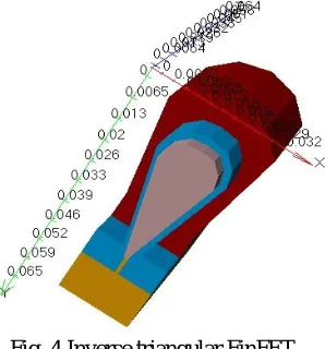
3.1 Inverse Triangular fin Structure
The triangular fin structure is kept upside down to get inverse triangular structure as shown in figure 4. Here the main advantage is that the ON current can be increased as the area at the top is increased. This top region is surrounded by gate.
Fig. 4 Inverse triangular FinFET
3.2 Concave and Convex fin Structures
(a) (b) Fig. 5 (a) Convex FinFET (b) Concave FinFET
The proposed concave and convex FinFETs provide better leakage control than the normal bulk-Si FinFETs or tri-gate devices with rectangular or trapezoidal fins. It is due to the formation of quasi-surrounding gate electrodes on concave and convex fins by a special Si etch process. Concave structure is curving in structure whereas; convex structure is curving out structure. The sharp edges are rounded to avoid the corner effect. Ion/Ioff ratio is also improved. The
difficulty lies in the fabrication of these structures because of the curved structure.
Concave structure can be formed by placing two triangular FinFETs, bottom one is placed straight and the top one is inversed. Convex fin is obtained by placing an inverse triangle at the bottom and the straight one at the top. So the fabrication of both structures is similar.
IV.RESULTS AND DISCUSSION
The analysis is done on 22nm bulk FinFET Technology model. Simulations are done by TCAD.
4.1 Threshold Voltage
Threshold voltage, Vth is extracted using the maximum transconductance method with Vd = 0.05 V. The variation of Vth
with top width and doping concentration is studied [9].
Fig. 6 Threshold voltage comparison of nFinFET as a function of fin shape
400 420 440 460 480 500 520
T
h
re
sh
o
ld
V
o
lt
ag
e
(m
V
)
Threshold Voltage v/s fin shape
From the figure 6, it is observed that threshold voltage increases when Wtop decreases from 15 nm to 1 nm. Vth is within
the range 496 mV to 506 mV when Wtop varies from 15 nm to 1 nm. This is due to quantum confinement. In the case of
concave and convex FinFETs, the threshold voltage has taken an optimum value, whereas in the case of inverse triangular FinFET, the value has lowered to 450 mV. Threshold voltage increases with increase in doping concentration. For an intrinsic semi conductor the threshold voltage will be negative.
4.2 Subthreshold Swing
The Subthreshold swing, SS decreases when Wtop decreases and increases when doping concentration increases [2].
The SS is extracted at a gate voltage (Vg) of 0.3 V.
Fig. 7 Subthreshold Swing comparison of nFinFET as a function of fin shape
From the figure 7, it is clear that SS is directly proportional to the top width of the fin. Subthreshold swing total range is 11 mV/decade by fin shape variation from rectangular (Wtop = 15 nm) to triangular (Wtop=1 nm). Subthreshold swing
is less than 85 mV/decade. In the case of concave and convex FinFETs, the SS is lowered below 60 mV/decade.
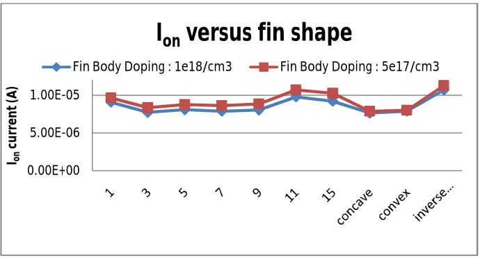
4.3 Ion Current
Ion current is extracted when Vgs and Vds is Vdd.
25 33 41 49 57 65 73 81 89
Su
b
th
re
so
ld
S
w
in
g
(m
V
/d
ec
)
Subthreshold Swing v/s fin shape
Fin Body Doping : 1e18/cm3 Fin Body Doping : 5e17/cm3
0.00E+00 5.00E-06 1.00E-05
Ion
cu
rr
e
n
t
(A
)
I
on
versus fin shape
Figure 8 shows that Ion current decrease as the fin width decreases. It is because of the decrease in charges per area. As
doping is increased,Ion decreases due to mobility degradation.
4.4 Leakage Current and Ion/ Ioff Ratio
MOSFET’s drain leakage current or off-state current (Ioff) is the drain currentwhen no gate voltage is applied. It is the
drain to source current which is extracted when Vgs=0 and Vds = Vdd.
Ioff current also decreases as the fin width decreases because the leakage current occurs at the middle of the fin, which
is the more remote area from the gate. But as fin width decreases, the middle part of the fin has more control from the gate, so the leakage current decreases.
Fig. 9 Leakage current comparison of nFinFET as a function of fin shape
Figure 9 indicates as width increases, leakage increases. But in concave and convex FinFETs leakage is reduced more. Therefore, varying Wtop between 1 nm to 15 nm produces a multitude of transistor design choices.
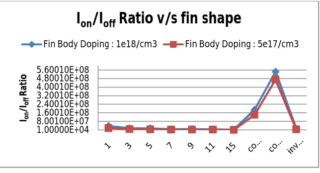
Fig. 10 Ion/Ioff ratio comparison of nFinFET as a function of fin shape
The reduction in Ion with respect to the decrease in width is less compared to the reduction in Ioff. Therefore, Ion/Ioff
monotonically increases as Wtop decreases as seen in figure 10. Concave and convex FinFETs has better Ion/Ioff as
compared with triangular and rectangular FinFETs. When the doping increases, mobility degradation occurs, hence Ion
1.0000E-15 5.0010E-12 1.0001E-11 1.5001E-11
Le
ak
a
ge
C
u
rr
e
n
t
(A
)
Leakage current v/s fin shape
Fin Body Doping : 1e18/cm3 Fin Body Doping : 5e17/cm3
1.00000E+04 8.00100E+07 1.60010E+08 2.40010E+08 3.20010E+08 4.00010E+08 4.80010E+08 5.60010E+08
Ion
/Io
ff
R
at
io
I
on/I
offRatio v/s fin shape
decreases. As we increase the channel doping drive current reduces almost linearly, but off state current decreases exponentially. This leads to increase in Ion/Ioff ratio very sharply.
Table 1 shows the comparison results of partially cylindrical, triangular, concave, convex and inverse triangular FinFETs in response with parameters like threshold voltage, subthreshold swing, leakage current, Ion current and Ion/Ioff
ratio.
Table 1 Comparison results
Parameters Partially
cylindrical Triangular Concave Convex
Inverse triangular Threshold
Voltage (mV) 496.797 505.993 493.395 490.757 465 Subthreshold
Swing (mV/dec) 85.29 74.04 52.41 26.20 74.30 Leakage current
(pA) 3.511 0.2576 0.04085 0.01450 0.9154 Ion current (µA) 9.216 9.066 7.631 7.889 10.68
Ion / Ioff ratio
2.624E+0
6 3.518E+07 1.867E+08 5.440E+08 1.167E+07
From the table 1 it is clear that the threshold voltage is in the range of 465 mV to 495 mV. Subthreshold swing is within the range of 26 mV/decade to 85 mV/decade. The leakage current is reduced in triangular by 90% when compared to partially cylindrical FinFET. It has reduced further to 94% in case of convex FinFET and 84% in case of concave FinFET. The ON current has reduced to 15% in concave and convex FinFETs when compared with triangular FinFET. It has increased to 15% in inverse triangular FinFET when compared to triangular FinFET.
VI.CONCLUSION
Triple-gate FinFET devices are one of the most assuring successors of conventional MOSFET devices. It is observed that rounding the corners of the fin reduces leakage current.
Fin shape has considerable impact on leakage performance. There is 90% reduction in leakage if the fin shape changes from rectangular to triangular. There is further 94% reduction in leakage current from triangular to concave and convex fin shapes. By using inverse triangular FinFET large drive current can be achieved. It has increased to 15% in inverse triangular FinFET when compared to triangular FinFET. The threshold voltage is in the range of 465 mV to 495 mV. Subthreshold swing is within the range of 26 mV/dec to 85 mV/dec.
REFERENCES
[1] Anindya Jana "Extraction of RF parameters of Bulk FinFET" thesis, 2010.
[2] Hasanur R. Khan, Denis Mamaluy, and Dragica Vasileska, “Simulation of the Impact of Process Variation on the Optimized 10-nm FinFET,” IEEE Trans. Electron Devices, vol. 55, no.8, Aug.2008.
[3] Kaushik Roy, Fellow, IEEE, Saibal Mukhopadhay And Hamid Mahmoodi-Meimand, "Leakage Current Mechanisms and Leakage Reduction Techniques in Deep-Sub micrometer CMOS Circuits", 2002.
[4] Mayur Bhole, Aditya Kurude, Sagar Pawar "FinFET- Benefits, Drawbacks and Challenges" International Journal Of Engineering Sciences and Research Technology, 2013.
[5] M. Pavan Kumar, Santosh Kr. Gupta, Madhumita Paul "Corner Effects in SOI-Tri-gate FinFET structure by using 3D Process and Device Simulations" IEEE 2010.
[6] Nor Zaidi Haron Said Hamdioui "Why is CMOS scaling coming to an END?" IEEE, 2010.
[8] Sanjeev Rai, Jyotsna Sahu, Wanjul Dattatray, R. A. Mishra, and Sudarshan Ti-Wari "Modelling, Design, and Performance Comparison of Triple Gate Cylindrical and Partially Cylindrical FinFETs for Low-Power Applications "International Scholarly Research Network ISRN Electronics Volume 2012.
[9] Shiying Xiong and Jeffrey Bokor, “Sensitivity of Double-Gate and FinFET Devices to Process Variations,” IEEE transactions on electron devices, vol. 50, no. 11, November 2003
[10] Suman Lata Tripathi and R. A. Mishra,"Design of 20 nm FinFET structure with round fin corners using side surface slope variation”, Journal of Electron Devices, Vol. 18, 2013.
![Fig. 2 Conventional FinFET [8]](https://thumb-us.123doks.com/thumbv2/123dok_us/7783450.1286682/2.595.257.335.389.476/fig-conventional-finfet.webp)