APWM Based Multiple Output ZVS DC/DC
Converter
N.Rajendran, S.P.Vijayaragavan
Assistant Professor, Department of Electrical Engineering, Bharath University, Chennai, Tamil Nadu, India
Assistant Professor, Department of EEE, Bharath University, Chennai, Tamil Nadu, India
ABSTRACT: This project presents a new soft-switching dc/dc converter with series-connected transformers to implement the features of ZVS, low voltage stress for MOSFETs. The converter includes two half-bridge circuits connected in series to limit the voltage stress of MOSFETs at one-half of the input voltage. The output sides of four circuits are connected in series and parallel to primary circuit. The proposed multi output converter shows excellent performance in terms of its output regulation from no-load to full-load conditions and its provide multi output capability .
KEYWORDS: DC–DC converter, Asymmetrical half-bridge, multi output converter, soft switching.
I. INTRODUCTION
POWER FACTOR corrections (PFCs) have been widely used in modern power converters to compensate the reactive power and eliminate the ac current harmonics at the utility side. For a three-phase 380-V PFC converter or a single-phase PFC converter with wide input voltage range in South Africa orIndia, the dc bus voltage may be greater than 600 V. Therefore,MOSFETs with 600-V voltage stress and low turn-on resistancecannot be used in the rear dc/dc stage. Although high-voltageMOSFETs such as those with 900-V voltage stress can beused in the rear dc/dc converter, the disadvantages of high voltage MOSFETs are high cost and large turn-on resistance By using more MOSFETs, split capacitors, the voltagestress of each MOSFET can be reduced to one-half of the dcbus voltage. Therefore, MOSFETs with 600-V voltage stress can be used in the rear dc/dc converter for high-input-voltage was normally adopted to generate four PWM signals for power switches with zero-voltage switching (ZVS) turn-on at the designed load range.[1-4] A isolation transformers are adopted in the secondary side for low or high-voltage applications. Soft-switching techniques [5], [8]–[14] have been developed and proposed for the past 20 years to reduce Soft-switching losses and increase circuit efficiency.
This paper presents a new soft-switching dc/dc converter for high-input-voltage applications. The main advantages of the proposed converter are low switching losses, ZVS turn-on, andlow voltage stress on MOSFETs. Two capacitors and two half-bridge circuits are connected in series at the high-voltage sideto clamp the voltage stress of MOSFETs at one-half of the dc bus voltage. Asymmetric PWM(APWM) is adopted to control four MOSFETs so that the general PWM IC with three isolated gate drives can be usedin the proposed circuit. Based on the resonant behavior by the output capacitance of MOSFETs and the resonant inductance, MOSFETs can be turned on at ZVS. Experiments with a1-kW prototype are presented to verify the effectiveness of theproposed converter.
II. CIRCUIT CONFIGURATION
ISSN (Print) : 2320 – 3765 ISSN (Online): 2278 – 8875
I
nternational
J
ournal of
A
dvanced
R
esearch in
E
lectrical,
E
lectronics and
I
nstrumentation
E
ngineering
(An ISO 3297: 2007 Certified Organization)
Vol. 4, Issue 6, June 2015
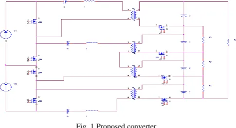
the third circuit include Vin , S1 –S4 , Cr1 –Cr4 ,C2 , Lr2 , T3 , T4 , S5 –S8 , Lo1 , and Lo2 . Co and Ro denotethe output capacitance and load resistance, respectively. C1 –C3 are the dc blocking capacitances.
Fig. 1.Proposed converter .
The dc blocking voltagesVC1 –VC3 are related to the duty ratio of MOSFETs. Cr1 –Cr4are the output capacitances of MOSFETs S1 –S8 , respectively.Lr1 –Lr3 are the resonant inductances. Lm1 –Lm4 are the magnetizing inductances of transformers T1 –T4. The APWM scheme is used to control MOSFETs S1 –S4 . S5 - S8 have the same pwm signal.S1 and S4 have the same PWM signals, and S2 andS3 have the same PWM waveforms. However, S1 and S2 are complementary to each other with a dead time to allow ZVS operation. Therefore, the PWM signals of S1 –S4 can be easilygenerated by an analog PWM IC and three isolated gate drivers.The voltage stress of S1 –S4 is clamped to Vin /2. Since the secondary windings of four circuits are connected in series, four output capacitors currents are automatically balanced for high-output-current applications.[5-8]
III .CIRCUIT OPERATING PRINCIPLE
The theoretical waveforms of the proposedconverter in one switching cycle. The duty cycle of S1 and S4 is δ, and the duty cycle of S2 and S3 is 1 − δ. Before the system analysis, the following assumptions are made:
1) MOSFETsS1 –S4 and diodes S5 –S8 are ideal; 2) Lm1 = Lm2 = Lm3 =Lm , and Lo1 = Lo2 = Lo ; Lm4 = Lm , Lr1 = Lr2 = Lr3
3) the turn ratio of transformers T1 –T4 is n = np /ns1 =np /ns2 ;
4) Cr1 = Cr2 = Cr3 = Cr4 = Cr and C1 = C2 = Cr ; and
5) the energy stored in resonant inductorsC3 = Ccis greater than the energy stored in resonant capacitors such thatthe ZVS turn-on of all switches can be achieved. Based on theON / OFF states of S1 –S8 , there are four operationmodes in one switching cycle. [9-10]
Mode 1 [t0 ≤ t < t1] ; During this interval, all switches i.e. S1,S2,S3,S4,S5,S6,S7,S8 turned off.c1,c2,c3 are
charged in this mode.Lr1,Lr2 ,Lr3 are almost constant.c4,c5,c6,c7 discharged in this time.
Mode 2 [t1 ≤ t < t2 ; Fig. 3(b)]: At t1 ]: During this interval, the antiparallel switches of S1 and S4 are conducting at t2. Before iS1 and iS4 are positive, S1 and S4 must be turned on to achieve ZVS. S2,S3 and S5-S8 switches are also on condition capacitors can charge in this mode .at the same time Lr1, Lr3 stores the energy . switches s2,s3 turned off.
Mode 3: [t2 ≤ t < t3] ]: During this interval, the antiparallel switches of S1 and S4 are OFF. S2,S3 switches are On condition and S5-S8 switches are OFF condition, capacitors are discharge in this mode.
Fig.(2a)
Fig.(2b)
Fig(2c)
Fig(2d)
ISSN (Print) : 2320 – 3765 ISSN (Online): 2278 – 8875
I
nternational
J
ournal of
A
dvanced
R
esearch in
E
lectrical,
E
lectronics and
I
nstrumentation
E
ngineering
(An ISO 3297: 2007 Certified Organization)
Vol. 4, Issue 6, June 2015
Experimental results are provided to demonstrate the effectiveness of the proposed converter. The circuit specificationsof a laboratory prototype are Vin = 480–600 V, Vo1 = 45 V, Vo2 = 8.4, Vo3 = 7.8 V ,Vo4 = 13.5 Vand Po = 1 kW. The switching frequency fs is 100kHz.The nominal input voltage Vin, nom is 540 V. The maximumduty cycle of S1 and S4 is selected as 0.45 for the case ofVin = 480 V and Po = 1 kW. MOSFETs IRFP460 are used forS1 –S4 . The dc blocking capacitances are C1 = C3 = 330 nFand C2 = 660 nF. The resonant inductances are Lr1 = Lr3 = 18 μH and Lr2 = 36 μH. The fast recovery diodes U30D20Care used for D1 –D6 . The turn ratio of transformers T1 – T4 is34 : 5 : 5. The magnetizing inductance of T1 –T4 is 870 μH. Theoutput capacitance is Co = 6200 μF. The output inductancesare Lo1 = Lo2 = 46 μH. The measured PWM signals of S1 –S4at full load and the different input voltages are shown in Fig. 4a.Fig. 4b shows the measured gate voltage, drain voltage, andswitch current of switches S1 and S2 at the nominal input voltage Vin = 540 V and 25%- to 100%-load conditions. The drain voltages vS1,ds and vS2,ds have been decreased to zero voltage before switches S1 and S2 are turned on. Thus, S1 and S2 are turned on at ZVS from 25% to 100% load. Since the switches S1 and S4 have the same PWM waveforms and S2 and S3 have the same PWM waveforms, it is clear that S3 and S4 are also turned on at ZVS. shows the measured waveforms of the gate voltage vS1,gs and the inductor currents iLr1 –iLr4at full load and the nominal input voltage. When switch S1 isin the ON state, the inductor currents iLr1 and iLr3 decrease,and iLr2 increases. On the other hand, inductor currents iLr1 and iLr3 increase and iLr2 decreases if switch S1 is in the OFFstate. Fig. 7 shows the measured waveforms of vS1,gs , vC1 , vC2 , and vC3 at full-load condition. When switch S1 is on, theinductor currents iLr1 and iLr3 are negative so that capacitorvoltages vC1 and vC3 decrease. However, inductor current iLr2is positive so that capacitor voltage vC2 increases. Fig. 8 shows
the measured waveforms of vS1,gs , iS5 –iS8 , iLo1 , and iLo2 at full-load condition. The load current Io is equally supplied by output capacitors currents iCo1 and IC4 .[11-13]
V. SIMULATION RESULTS
A four-stage multiple output voltage of the APWM DC-DC converter for the simulation as shown in Fig.3.MATLAB/SIMULINK is used for simulation. The system is designed based on the the system specifications and the components as mentioned in experimental results .[14-17]
Fig(4a)
Fig.(4b)
ISSN (Print) : 2320 – 3765 ISSN (Online): 2278 – 8875
I
nternational
J
ournal of
A
dvanced
R
esearch in
E
lectrical,
E
lectronics and
I
nstrumentation
E
ngineering
(An ISO 3297: 2007 Certified Organization)
Vol. 4, Issue 6, June 2015
Fig.(4d)
Fig.4.(a)Input voltage (b)Switching Waveform.(c)Switch across the voltage for S1.(d) output voltage of the Dc-Dc converter and converter across load.
VI. CONCLUSION
This project has presented a new dc/dc converter with series connected transformers. The main functions of the proposed converter are as follows: 1) ZVS turn-on for all power switches; and 2) low voltage stress of power switches with a series half-bridge converter. Two split capacitors and two half-bridge converter circuits connected in series were used at the high-voltage side to limit the voltage stress of power switches at one-half of the input voltage. Thus, the MOSFETs can be used in high input voltage applications to achieve high switching frequency, low converter size, and high circuit efficiency.
Three APWM converters were used in the primary side, and the output sides of four circuits are connected in series and parallel to primary circuit. The proposed multi output converter shows excellent performance in terms of its output regulation conditions and its provide multi output capability .
REFERENCES
1. W. Chen and X. Ruan, “Zero-voltage-switching PWM hybrid full-bridge three-level converter with secondary-voltage clamping scheme,” IEEETrans. Ind. Electron., vol. 55, no. 2, pp. 644–654, Feb. 2008.
2. H. Ertl, J. W. Kolar, and F. C. Zach, “Analysis of a multilevel multicell switch-mode power amplifier employing the flying-battery concept,”IEEE Trans. Ind. Electron., vol. 49, no. 4, pp. 816–823, Aug. 2002.
3. Subha Palaneeswari M., Abraham Sam Rajan P.M., Silambanan S., Jothimalar, "Blood lead in end-stage renal disease (ESRD) patients who were on maintainence haemodialysis", Journal of Clinical and Diagnostic Research, ISSN : 0973 - 709X, 6(10) (2012) pp.1633-1635.
4. Sharmila S., Rebecca L.J., Saduzzaman M., "Effect of plant extracts on the treatment of paint industry effluent", International Journal of Pharma and Bio Sciences, ISSN : 0975-6299, 4(3) (2013) pp.B678-B686.
5. Jeyanthi Rebecca L., Dhanalakshmi V., Sharmila S., "Effect of the extract of Ulva sp on pathogenic microorganisms", Journal of Chemical and Pharmaceutical Research, ISSN : 0975 – 7384 , 4(11) (2012) pp.4875-4878.
6. Sharmila D., Saravanan S., "Efficacy of lead on germination growth and morphological studies of Horse Gram (Dolichos biflorus Linn)", Journal of Chemical and Pharmaceutical Research, ISSN : 0975 – 7384 , 4(11) (2012) pp.4894-4896.
7. Saduzaman M., Sharmila S., Jeyanthi Rebecca L., 'Efficacy of leaf extract of Moringa oleifera in treating domestic effluent", Journal of Chemical and Pharmaceutical Research, ISSN : 0975 – 7384, 5(2) (2013) pp.139-143.
8. H. Ertl, J. W. Kolar, and F. C. Zach, “A novel multicell DC–AC converter for applications in renewable energy systems,” IEEE Trans. Ind. Electron.,vol. 49, no. 5, pp. 1048–1057, Oct. 2002.
10. Y. Jiang, Z. Chen, and J. Pan, “Zero-voltage switching phase shift full bridge step-up converter with integrated magnetic structure,” IET Power Electron., vol. 3, no. 5, pp. 732–739, Sep. 2010.
11. B. R. Lin and S. F. Wu, “ZVS resonant converter with series-connected transformers,” IEEE Trans. Ind. Electron., vol. 58, no. 8, pp. 3547– 3554,Aug. 2011.
12. Lingeswaran, K., "Microcontroller-based MPPT control for standalone PV system with sepic converter", Middle - East Journal of Scientific Research, v-20, i-8, pp:945-950, 2014.
13. Thamarai, P., Karthik, B., Kumaran, E.B., "Optimizing 2:1 MUX for low power design using adiabatic logic", Middle - East Journal of Scientific Research, v-20, i-10, pp:1322-1326, 2014.
14. Jayalakshmi, V., "Wireless sensor network for performance monitoring of electrical machine", Middle - East Journal of Scientific Research, v-20, i-8, pp:996-999, 2014.
15. Prasad, K.S., "A design towards smart batteries", Middle - East Journal of Scientific Research, v-20, i-10, pp:1318-1321, 2014.