Modular Multilevel DC/DC Converters with
Phase-Shift Control Scheme for HVDC based system with
Closed loop Control
VIKRAMKUMAR MUTHYALA
M-tech Student Scholar
Department of Electrical & Electronics Engineering, Elleki Institute Of Engg. And Technology, PATANCHERU,
MEDAK DISTRICT - 502305; Telangana, India.
MR. PRASAD
Assistant Professor
Department of Electrical & Electronics Engineering, Elleki Institute Of Engg. And Technology, PATANCHERU,
MEDAK DISTRICT - 502305; Telangana, India.
Abstract-In this paper, by investigating the topology derivation principle of the phase-shift-controlled three-level dc/dc converters, the modular multilevel dc/dc converters, by integrating the full-bridge converters and three-level flying capacitor circuit, are pro-posed for the high step-down and high power dc-based systems. The high switch voltage stress in the primary side is effectively reduced by the full-bridge modules in series. Therefore, the low-voltage-rated power devices can be employed to obtain the benefits of low conduction losses. More importantly, the voltage auto balance ability among the cascaded modules is achieved by the inherent flying capacitor, which removes the additional possible active components or control loops. In addition, zero-voltage-switching performance for all the active switches can be provided due to the phase-shift control scheme, which can reduce the switching losses. The circuit operation and converter performance are analyzed in detail. Finally, the performance of the presented converter is verified by the simulation and experimental results from a 2-kW prototype. The proposed concept is implemented with closed loop control to attain desired voltage using MATLAB/SIMULINK software.
Index Terms—Input voltage auto balance, modular multilevel dc/dc converter, phase-shift control scheme, zero-voltage switching (ZVS).
I. INTRODUCTION
In recent years a dc to dc converter with high performance is needed for HVDC(High Voltage Direct Current) based systems such as fuel cell power systems and distributed power systems[1-2].Conventional dc to dc converter is not suitable for such applications due to lack of commercial high voltage high performance power MOSFETS. For instance a typical railway system is considered. They are provided by DC transmission lines with voltage levels of 600,750,1500 or 3000v.This high voltage is inverted to 440v, and further rectified to 110v dc for batteries. This 110v dc is again stepped down to 72v,48v,36v and 24v for auxiliary equipments. This multiple conversion stages of voltage leads to low conversion efficiency. An attempt has been made to step down voltage at high switching frequency in single step to improve conversion efficiency .Insulated Gate Bipolar
Transistors(IGBTs) and metal Oxide Se miconductor FETS(MOSFETS) are dominantly used switches for medium voltage or high voltage applications.If only high input voltage is a factor , IGBTs are preferred as they have high blocking voltage capability but it limits to only low switching frequency which is an obstacle to achieve high power density. MOSFETS are the unique selection for high switching frequency operation. Though 4000v rated mosfets available they have high ON resistance which results in conduction losses. So in order to achieve high performance converter an attempt has been made to derive advanced converter topologies. To reduce voltage stresses on the devices ISOP(Input Series Output Parallel) converters was proposed in [3]. Many converter topologies are discussed in [4-8] to reduce switch voltage stresses. But the conversion efficiency is unfortunately affected because of hard switching operation of above proposed converters. Another converter has been proposed in [9] which uses snubber circuit to achieve ZVS, of course voltage balance is achieved by external closed loop circuits which increases the complexity of circuit.
In this paper, the flying capacitor and full-bridge converters are combined and integrated to derive the advanced modular multilevel dc/dc converters for the high step-down and high power dc-based conversion applications. Due to the charging and discharging balance of the built-in flying capacitor, the input voltage auto balance ability is naturally realized, and overcomes the input voltage imbalance. Furthermore, the phase-shift control strategy can be used to achieve the soft-switching operation and reduce the switching losses. The concept of modular multilevel dc/dc converters may provide a clear picture on high-voltage dc/dc topologies for the dc-based distribution and micro grid systems.
II. DERIVATION LAW OF MODULAR MULTILEVEL CONVERTERS
is well known that the neutral-point-clamped (NPC) converters and flying capacitor-based converters are the major multilevel topologies for the voltage and high-power applications[10]. For the conventional NPC converters with pulse width modulation control, the abnormal operation condition, such as the mismatch in the gate signals, may cause the voltage imbalance of the input capacitors. Therefore, the converter reliability is impacted. Further more, the phase-shift control scheme is not suitable for the conventional NPC converters, which leads to large switching losses. Fortunately, by inserting a small flying capacitor parallel connected with the clamping diodes, the input capacitor voltages are automatically shared because the flying capacitor can be directly parallel with the series input capacitors alternatively[11].
More importantly, the phase-shift control strategy can be easily applied to achieve zero-voltage-switching (ZVS) operation without adding any other power components. The phase-shift controlled three-level dc/dc converter is plotted in Fig. 1(c). From another point of view, the phase-shift-controlled TLC can be regarded as the combination and integration of the three-level NPC converter as given in Fig. 1(a) and the three-level flying capacitor-based circuit as shown in Fig. 1(b), where the input capacitors and active power switches are reused and shared to reduce the circuit complexity. As a result, the advantages of the NPC converter and flying capacitor-based circuit are kept whereas their inherent disadvantages are effectively avoided. Many further improve ments are made for the combined phase shift-controlled TLC by adding some active or passive components to extend the soft-switching operation range[12-15].
Fig.1. Derivation of novel TLC: (a) NPC TLC, (b) flying capacitor-based TLC, and (c) phase-shift-controlled combined TLC.
Based on the previously summarized combined multilevel derivation principle, it is innovative and attractive to consider the possibility of combination of the other funda mental multilevel topologies. For example, the cascaded full-bridge converter, or the ISOP full-bridge
converter, and the three-level flying capacitor-based converter are combined and integrated to derive the advanced modular multilevel dc/dc converters, which is detailed illustrated in Fig. 2. The time sequence of the leading leg in the phase-shift-controlled full-bridge converters is kept constant and only the phase of the lagging leg is shifted to regulate the output voltage. This indicates that the leading legs of the cascaded full-bridge converter can be assembled with the three-level flying capacitor-based converter to achieve the input voltage auto balance. And the lagging legs of the cascaded full bridge converter are still kept unchanged to provide adequate control freedom to achieve fast and accurate output voltage regulation.
Consequently, for the proposed modular multilevel dc/dc converters, the big concern of the input-voltage imbalance existed in the ISOP converters is completely overcome due to the built-in flying capacitor. More importantly, the derived modular multilevel dc/dc concept can be easily put forward to N-stage converters by stacking the full-bridge power modules in series in the primary side to satisfy the growing bus voltage in the dc-based distribution and micro grid systems. In view of the phase-shift-controlled topologies, the aforementioned optimized strategies for the phase-shifted-controlled TLCs can be directly transferred to the derived modular multilevel dc/dc converters to generate a fa mily of high performance topologies for the voltage and high-power applications. It can be concluded that this modular multilevel converter concept is one of the general solutions for the high-voltage and high-power dc/dc topology origination.
Fig.2. Derivation of the proposed modular multilevel dc/dc converter: (a) cascaded full-bridge converter, (b) flying capacitor-based TLC, and
(c) proposed modular multilevel dc/dc topology
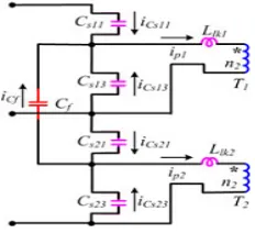
rectifier is applied as an exa mple to explore the circuit performance of the proposed modular multilevel configuration, which is illustrated in Fig. 3. In the primary side, the capacitors C1and C2are used to split the high input voltage, S11−S14are the power switches of the top full-bridge module, S21−S24form the bottom full-bridge module,Cs11−Cs24are the parasitic capacitors of the power switches, and Llk1and Llk2 are the leakage inductors of the transformers T1andT2, respectively. In the secondary side, Do11, Do12, Lf1, and Co1 are for the top full-bridge module and Do21, Do22, Lf2, and Co2 are for the bottom full-bridge module. ip1, ip2, iDo11, iDo12, iDo21, and iDo22are the primary and secondary currents through the windings of the transformers with the defined direction in Fig. 3. And is1and is2 are the filter inductors currents.
Fig.3. Proposed modular multilevel dc/dc converter with input voltage auto balance ability.
Fig.4. Key waveforms of the proposed converter.
A. Operation Analysis
The phase-shift control scheme is employed in the proposed converter to realize the ZVS performance of all the power switches, where S11,S13,S21, and S23 are the leading-leg switches and S12,S14,S22, and S24 are the lagging-leg switches. The key wavefor ms of the proposed converter are shown in Fig. 4. For the top full-bridge
module,S11 andS13 act with 0.5 duty cycle comple mentarily with proper dead time td, so as for the switches S12 andS14. The phase-shift angle between the leading and lagging switch pairs is defined as ϕ1.
The gate signal pattern of the bottom full-bridge module is similar to that of the top full-bridge module with the phase-shift angle ϕ2. Meanwhile, the leading switches pair S11 andS13 turns ON and OFF simultaneously with the switch pair S21 andS23, while the phase-shift angles ϕ1 and
ϕ2 are decoupled control freedoms for the output voltage regulation.
The mode 0 <ϕ1−ϕ2 <td is taken into consideration when analyzing the operation of the converter, and the equivalent operation circuits are depicted in Fig. 5. In order to simplify the analysis, the following assumptions are made: 1) all the power switches and diodes are ideal; 2) the parasitic capacitorsCs11−Cs24of the switches have the same value as Cs; 3) the voltage ripples on the divided input capacitorsC1,C2 and flying capacitors Cf are small due to their large capacitance; 4) the turns ratio of both transformers is N= n2:n1; and 5) the input voltage is balanced. There are 15 operation stages in one switching period. Due to the symmetrical circuit structure and operation, only the first eight stages are analyzed as follows.
Stage 1 [t0,t1]:Before t1, the switches S11,S14,S21, and S24are in the turn-on state to deliver the power to the secondary side. The output diodesDo11 andDo21 are conducted and the output diodesDo12 andDo22 are reverse biased. The flying capacitor Cf is in parallel with the input divided capacitor C1 to make VCf equal toVC1.
ip1(t) = ip1(to) + 2 (t – to) (1)
Stage 2 [t1,t2]:At t1, the turn-off signals of the switches
S11and S21are given. ZVS turn off for these two switches are achieved due to the capacitors Cs11 andCs21. Cs11 andCs21 are charged andCs13 andCs23 are discharged by the primary currents.
Stage 3[t2,t3]:At t2, the voltages of Cs13 andCs23 reach 0 and the body diodes ofS13andS23are conducted, providing the ZVS turn-on condition forS13andS23. The flying capacitor Cf is changed to be in parallel with the input divided capacitor C2. The primary currents are derived by
ip1(t) =
( )(3)
ip2(t) = ( ) (4)
Stage4[t3,t4]:At t3,S14turns off with ZVS.Cs14is charged andCs12 is discharged, leading to the forward bias of Do12; hence, the secondary currentis1 circulates freely through both Do11andDo12. ip1is regulated by
ip1(t) = ip1(t3) cos ω (t – t3) (5)
ω =
(6)
Stage 5 [t4,t5]:At t4, the turn-off signal ofS24comes. ZVS turn-off performance is achieved forS24. Similar to the previous time interval, Do21 and Do22 conduct simultaneously, thus leading to the transformer T2 short-circuit. ip2 is regulated by
ip2 (t) = ip2 (t4) cos ω (t – t3) (7)
ω =
Stage 6 [t5,t6]:Att5,Cs12is discharged completely and the anti parallel diode of S12 conducts, getting ready for the ZVS Turn-on ofS12. During this time interval, ip1 declines steeply duo to half-input voltage across the leakage inductor Llk1, ip1 is given by
ip1(t) = ip1 (t5) –
(t – t5) (9)
Stage 7 [t6,t7]:At t6,ip1 decreases to 0 and increases
reversely with the same slope throughS12 andS13. Cs22 is discharged completely and the anti parallel diode ofS22conducts. ip2 declines rapidly duo to half-input voltage across the leakage inductor Llk2.ip2is given by
ip2(t) = ip2(t6) – ( t – t6 ) (10)
Stage 8 [t7,t8]:At t7,ip2 decreases to 0 and increases
reversely throughS22 andS23. The current through the output diodeDo11 decreases to 0 and turns off. The output diodeDo21 turns off aftert8, and then a similar operation works in the rest stages.
B. Input Voltage Auto balance Mechanism
The input voltage imbalance is one of the major drawbacks for most multilevel converters and ISOP converters, which is mainly caused by the asymmetry of the component parameter difference and the mismatch of control signals. It has been carried out that the transformer turns ratio difference (N), leakage inductance distinction (Llk), and phase-shift angle mismatch (ϕ) are the main reasons for the input voltage imbalance in the steady state for the ISOP phase-shift-controlled converters
The input voltage auto balance mechanism of the proposed modular multilevel dc/dc converter is displayed in Fig. 6 and detailed elaborated as follows. According to the steady operation of the proposed converter, for the leading-leg switches, the switches S11 and S21 have the same time sequence and the switches S13 andS23 are operated synchronously. When S11 and S21 are turned ON, S13 and S23 are turned OFF accordingly, and the flying capacitor Cf is connected in parallel with the top input capacitor C1 as plotted in Fig. 5(a). This makes VCf equal toVc1. In the same way, as given in Fig. 5(b), the flying capacitor Cf is in parallel with the bottom input capacitor C2, when S13and S23 are in turn-on state. This denotes that VCf andVc2 are the same. The connection of Cf with C1 or C2 alternates with high switching frequency, which leads to the voltages on both the input capacitors automatically shared and balanced.
Fig.5. Input voltage auto balance mechanism: (a) Cf in parallel with C1 and (b) Cf in parallel with C2
IV. CONVERTER PERFORMANCE ANALYSIS A. Voltage Stresses of Switches
In the primary side, the voltage stress of the power switches S11−S24 is half of the input voltage owing to the series structure and the auto balance mechanism. As a result, the low voltage-rated power devices are available in the high input applications to restrict the conduction losses.
B. ZVS Soft-Switching Condition
1) Leading Legs: ZVS turn-off is achieved for the leading switches due to their intrinsic capacitors. In order to realize ZVS turn-on, enough energy is needed to charge and discharge the intrinsic capacitors. During the dead time interval [t1−t2], S11 andS21 are turned OFF; Cs11 andCs21 are charged andCs13 and Cs23are discharged as shown in Fig. 5. According to the Kirchoffs law, the following equations are derived:
iCs11 + iCs13 = ip1 - iCf (11)
iCs21 + iCs23 = ip2 + iCf (12)
It is reasonable to assume that ip1and ip2 are nearly constant during this period due to the short dead time. When the sum of VCs13 and VCs21 is not equal to VCf, Cf may be charged or discharged. The current iCf affects the ZVS performance of the power switches according to (11) and (12): 1) when Cf is discharged, iCf flows in the positive direction, and ZVS performance of S21 and S23 is improved but deteriorated for S11 andS13; and 2) when Cf is charged, iCf flows reversely, which improves the ZVS performance of S11 and S13but deteriorates that of S21and S23. Fortunately, Cf is much larger than Cs, making iCf small. Besides, the output filter inductance is reflected to the primary side and is in series with the resonant inductance. The energy of both the filter inductors and the
resonant inductors is sufficient to achieve ZVS for the leading switches. The output filter inductance is so large enough that the leading switches can realize ZVS turn-on even at light loads.
Fig. 6. ZVS equivalent circuit of leading switches during dead time
2) Lagging Legs: Similar with the leading switches, the lagging switches are able to realize ZVS turn-off by utilizing their intrinsic capacitors. However, only the energies of the resonant inductors are employed to achieve ZVS turn-on for the lagging switches
As the resonant inductance is quite smaller than the filter inductance, the achievement of the ZVS turn-on for the lagging switches is more difficult than the leading switches at light loads.
C. Duty Cycle Loss
During interval [t3–t7], Va1b1 is negative, and ip1 transits from the positive direction to the negative reflected filter inductance current. The secondary diodes Do11 andDo12 conduct simultaneously, making the secondary rectified voltage become 0. The duty cycle is lost during this time interval, the expression of which is derived by:
Dloss1 =
( )
≈ (13)
For the bottom full-bridge module, the duty cycle loss is similar to the top full-bridge module as given by
Dloss2 = ( ) ≈
_ (14)
Fig.7. Matlab/Simulink circuit of proposed system without flying capacitor
Fig.8.simulation waveform of capacitor voltages without flying capacitor.
Fig.9.Matlab/Simulink circuit of proposed system with flying capacitor.
Fig.10. simulation waveform of capacitor voltages with flying capacitor
Fig.12. simulation results of ZVS performance of switches.
Fig.13.simulation waveform of proposed system input voltage(600v) and output voltage(48v)
Fig.14.Matlab/Simulink circuit of closed loop system
Fig.15. simulation waveforms of closed loop system with desired outputs of 36v and 110v
VI. CONCLUSION
A new converter by integrating full bridge converters and flying capacitor based three level converter is proposed to reduce conduction losses and to attain autobalance of capacitor voltages.ZVS performance of switches is achieved with the help of phase shift control scheme,thereby reduction in switching losses.A closed loop control is implemented to this new converter to achieve desired output voltages for various auxiliary equipments. The modular multilevel dc/dc converter concept can be easily extended to N-stage converter with stacked full-bridge modules to satisfy extremely high-voltage applications with low-high-voltage-rated power switches.
REFERENCES
[1] P. M. Barbosa, F. Canales, J. M. Burdio, and F. C. Lee, “A three-level converter and its application to power factor correction,” IEEE Trans.Power Electron., vol. 20, no. 6, pp. 1319–1327, Nov 2005. [2] S. Byeong-Mun, R. McDowell, A. Bushnell, and J. Ennis, “A three-level DC–DC converter with wide-input voltage operations for ship-electricpower-distribution systems,” IEEE Trans. Plasma Sci., vol. 32, no. 5,pp. 1856–1863, Oct. 2004.
[3] S. Anand and B. G. Fernandes, “Optimal voltage level for DC microgrids,” inProc. IEEE Conf. Ind. Electron., 2010, pp. 3034–3039. [4] D. Salomonsson, L. Soder, and A. Sannino, “An adaptive control system for a DC microgrid for data centers,” IEEE Trans. Ind. Appl., vol. 44, no. 6, pp. 1910–1917, Nov./Dec. 2008.
[5] K. B. Park, G. W. Moon,, and M. J. Youn, “Series-input series-rectifier interleaved forward converter with a common transformer reset circuit for high-input-voltage applications,”IEEE Trans. Power Electron., vol. 26, no. 11, pp. 3242–3253, Nov. 2011.
[6] T. Qain and B. Lehman, “Coupled input-series and output-parallel dual interleaved flyback converter for high input voltage application,” IEEE Trans. Power Electron., vol. 23, no. 1, pp. 88–95, Jan. 2008. [7] C. H. Chien, Y. H. Wang, B. R. Lin, and C. H. Liu, “Implementation of an interleaved resonant converter for high-voltage applications,” Proc. IET Power Electron., vol. 5, no. 4, pp. 447–455, Apr. 2012.
[8] C. H. Chien, Y. H. Wang, and B. R. Lin, “Analysis of a novel resonant converter with series connected transformers, ”Proc. IET Power Electron., vol. 6, no. 3, pp. 611–623, Mar. 2013.
[9] T. T. Sun, H.Wang, H. S. H. Chung, S. Tapuhi, and A. Ioinovici, “A highvoltage ZVZCS DC-DC converter with low voltage stress,” IEEE Trans.Power Electron., vol. 23, no. 6, pp. 2630–2647, Nov. 2008. [10] J. Rodriguez, J. S. Lai, and Z. P. Fang, “Multilevel inverters: A survey of topologies, controls, and applications,” IEEE Trans. Ind. Electron.,vol. 49, no. 4, pp. 724–738, Aug. 2002.
[12] F. Canales, P. Barbosa, and F. C. Lee, “A voltage and zero-current switching three-level DC/DC converter,” IEEE Trans. Power Electron.,vol. 17, no. 17, pp. 898–904, Nov. 2002.
[13] B. R. Lin and C. H. Chao, “Analysis, design, and implementation of a soft-switching converter with two three-level PWMcircuits,” IEEE Trans.Power Electron., vol. 28, no. 17, pp. 1700–1710, Apr. 2013. [14] B. R. Lin and C. H. Chao, “Analysis of an interleaved three-level ZVS converter with series-connected transformers,” IEEE Trans. Power Electron.,vol. 28, no. 7, pp. 3088–3099, Jul. 2013.