A Low Power Binary to Excess-1 Code
Converter Using GDI Technique
Sri Phani Ramya . S1, Nimmy Maria Jose2
Assistant Professor, Dept. of ECE, ATRIA IT, Bangalore, Karnataka, India 1
Assistant Professor, Dept. of ECE, ATRIA IT, Bangalore, Karnataka, India 2
ABSTRACT: In this work a binary to excess-1 code converter is achieved by using GDI technique for the faster acceleration of the final addition in a hybrid adder. It is applied to the faster column compression multiplication using a combination of two design techniques: partition of the partial products into two parts for independent parallel column compression and acceleration of the addition using hybrid adder. The performance of the proposed design is compared with CMOS technology by evaluating the delay, power and transistor count with 180nm process technologies on
Tanner EDA tools. The results show the proposed design is significantly lower than CMOS technology.
KEYWORDS: GDI, CMOS, Hybrid adder, binary to excess-1 code converter.
I. INTRODUCTION
Code conversions are very essential in digital systems. Design of area and power efficient high speed data path logic systems are one of the most substantial areas of research in VLSI system design. In digital adders the speed of addition is limited by the time required to propagate a carry through the adder. The sum for each bit position in an elementary adder is generated sequentially only after the previous bit position has been summed and a carry propagated into the next position. The CSLA is used in many computational systems to elevate the problem of carry propagation delay. However the CSLA is not area efficient because it uses multiple pairs of RCA(ripple carry adder) to generate partial sum and carry by considering carry input(Cin=0, Cin=1), then final sum and carry are selected by multiplexers. The power and area of CSA can be reduced by using BEC-1 converter instead of RCA.
In order to achieve efficient low power VLSI circuits we are illustrating a method of designing a binary to Excess-1 code converter with GDI technique. A combinational circuit of adder with multiplexer, binary to excess-1 code converter and ripple carry adder is called a Hybrid adder. Here the binary to excess-1 converter has a complex layout using CMOS logic in terms of area, delay and power consumption. Hence an attempt has been made to develop a converter for low power consumption and less complexity. The rest of the paper is organized as follows: section II deals with the concept of GDI technique. In section III, the design of binary to ecess-1 code converter is discussed. Section IV emphasizes on simulation results and discussion. Session V draws conclusion.
II. BASIC GDI CONCEPT
“Fig: 1”. Basic GDI cell
Fig:1 represents the basic GDI cell (i.e.) inverter The GDI cell structure is different from the existing PTL techniques. It must be remarked that not all of the functions are possible in standard p-well CMOS process but can be successfully implemented in twin-well CMOS or silicon on insulator (SOI) technologies.
Table 1 describes the functions of basic gates. Table 2 shows the comparison between GDI and the static CMOS design in terms of transistors count. Any Boolean Function can be implemented using these universal gates.
III. DESIGN OF BINARY TO EXCESS-1 CONVERTER
A. Existing system
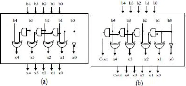
Code converters are very essential in digital systems. Here we are going to give the truth table for binary to excess-1 converter.Excess-1 converter is obtained by adding one to the binary value. The detailed structures of the 5-bit BEC
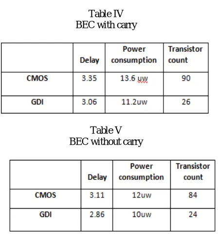
without carry (BEC) and with carry (BECWC) are shown in “Fig.2”. The BEC gets n inputs and generates n output; the
BECWC gets n input and generates n+1 output to give the carry output as the selection input of the next stage mux used in the final adder design. The function table of BEC and BECWC are shown in Table III.
Table III Truth table
Large bit sized multipliers requires multiple BEC and each of them requires the selection input from the carry output of the preceding BEC.
Therefore to generate the carry output from the BEC, an additional block is developed which is called BECWC (BEC With Carry). The detailed structures of the 5-bit BEC without carry (BEC) and with carry (BECWC) are shown “ Fig. 2(a) and Fig. 2(b)”.
B. Proposed system
It can be seen that large number of functions can be implemented using the basic GDI cell. Understanding of GDI cell properties demands a deeper operational analysis of the basic cell. Some of the digital circuits are implemented using 180nm CMOS process and the comparison is carried out between the standard CMOS logic and GDI Technique. In this proposed design the “Fig. 2(a) and Fig. 2(b)” were implemented using GDI. The following session describes the individual block representation of binary to excess-1 code converter.
1. Inverter
The design of GDI inverter using 180nm process is shown in “Fig.3”. 2 transistors are used in GDI as equal to CMOS.
Fig.3 GDI inverter
2. AND gate
The AND gate is implemented in GDI using 180nm process technology. 2 transistors are used in GDI technique while 6 transistors in standard CMOS technology. The implementation is shown in “Fig.4”.
Fig.4 AND gate
3. XOR gate
XOR Gate is implemented using 180nm technology and the comparison is done among standard CMOS and GDI Techniques. Among the implemented techniques GDI consumes least power and the 4 transistors while 16 transistors using CMOS. The implementation is shown in “Fig. 5”.
Fig.5 XOR gate
Table IV BEC with carry
Table V BEC without carry
These are the outputs of basic GDI cell without employing any level restoring circuits at their outputs. The compared results summarize the enhanced performance of the proposed design for with carry and without carry are shown in Table IV and V. The power consumption of the proposed BEC for the 5-bit word size is 16% less when compared to CMOS. With increasing word size the difference in power requirement of the proposed BEC decreases. The delay values clearly indicate that the proposed BEC is 8% faster than the regular, also with increasing word size the percentage reduction of the delay increases.
V. CONCLUSION
A novel GDI technique for low power design was presented. Reduction of power in code converters has great importance in digital systems. The performance parameters like power, delay and transistor count are determined, analyzed, verified in GDI and compared with the existing CMOS technology.
VI. FUTURE SCOPE
Major application of BEC is to achieve faster acceleration of final addition in hybrid adder which is a combination of MBEC (MUX and BEC) and RCA (ripple carry adder). We hope the presented results will encourage further research activities on GDI technique.
REFERENCES
1. V. G. Oklobdzija and D.Villeger, “Improving Multiplier Design by Using Improved Column Compression Tree and Optimized Final Adder in CMOS Technology”, IEEE transactions on Very Large Scale Integration (VLSI) systems, Vol. 3, no. 2, June 1995.
2. J. P. Uyemura, “Circuit Design for CMOS VLSI”. Norwell, MA: Kluwer Academic, 1992, pp. 88–129.
3. P. Chandrakasan, S. Sheng, and R. W. Brodersen, “Low- powerCMOS digital design,” IEEE J. Solid-State Circuits, vol. 27, pp. 473–484, Apr. 1992.
4. V. Adler and E. G. Friedman, “Delay and power expressions for a CMOS inverter driving a resistive-capacitive load,” Analog Integrated. Circuits Signal Process., vol. 14, pp. 29–39, 1997.
5. B.Parhami, "Computer Arithmetic", Oxford University Press, 2000.
6. E. E. Swartzlander, Jr. and G. Goto, "Computer arithmetic," The Computer Engineering Handbook, V. G. Oklobdzija, ed., Boca Raton, FL: CRC Press, 2002.
7. S. Wallace, “A Suggestion for a Fast Multiplier,” IEEE Transactions on Electronic Computers, Vol. EC-13, pp. 14-17, 1964.
8. Luigi Dadda, “Some Schemes for Parallel Multipliers,” Alta Frequenza, Vol. 34, pp. 349-356, August 1965.
9. K.C. Bickerstaff, E.E. Swartzlander, M.J. Schulte,” Analysis of column compression multipliers”, Proceedings of 15th IEEE Symposium on Computer Arithmeitc,2001.
10. W. J. Townsend, Earl E. Swartzlander and J.A. Abraham,“A comparison of Dadda and Wallace multiplier delays”, Advanced Signal Processing Algorithms, Architectures and Implementations XIII. Proceedings of the SPIE, vol. 5205, 2003, pages 552-560.