e-ISSN: 2278-067X, p-ISSN: 2278-800X, www.ijerd.com
Volume 11, Issue 10 (October 2015), PP.01-05
High Speed Time Efficient Reversible ALU Based Logic Gate
Structure on Vertex Family
1
Vivek Hardaha, prof.
2Paresh Rawat, prof.
3Saima Ayyub
Truba College of Science and Technology, Bhopal
Abstract:- Programmable reversible logic is emerging as a prospective logic design style for implementation in modern nanotechnology and quantum computing with minimal impact on circuit heat generation. Recent advances in reversible logic using and quantum computer algorithms allow for improved computer architecture and arithmetic logic unit designs. In this paper, the two novel 4*4 reversible logic gates (MRG and PAOG) are used with minimal delay, and may be configured to produce a variety of logical calculations on fixed output lines based on programmable select input lines. The proposed ALU design is verified and its advantages over the only existing ALU design are quantitatively analyzed. The proposed design is synthesized using Xilinx ISE software and simulated using MODEL SIM 6.5b.
Keywords:- Reversible Gates, Arithmetic Unit (ALU), Garbage Output, Quantum Cost
I.
INTRODUCTION
In modern VLSI system power dissipation is very high due to rapid switching of internal signals. The complexity of VLSI circuits increases with each year due to packing more and more logic elements into smaller volumes. Hence power dissipation has become the main area of concern in VLSI design. Reversible logic has its basics from thermodynamics of information processing. According to this, traditional irreversible circuits generate heat due to the loss of information during computation. In order to avoid this information loss the conventional circuits are modeled using reversible logic. Landauer [1961] showed that the circuits designed using irreversible elements dissipate heat due to the loss of information bits [1]. It is proved that the loss of one bit of information results in dissipation of KT*log2 joules of heat energy where K is the Boltzmann constant and T is the temperature at which the operation is performed. Benett [1973] showed that this heat dissipation due to information loss can be avoided if the circuit is designed using reversible logic gates [2]. A gate is considered to be reversible only if for each and every input there is a unique output assignment. Hence there is a one to one mapping between the input and output vectors. A reversible logic gate is an n –input, n- output device indicating that it has same number of inputs and outputs. A circuit that is built from reversible gates is known as reversible logic circuit. In this paper, we design a 16 bit reversible ALU that can perform eight operations simultaneously. The eight operations include addition, subtraction, AND, NAND, OR, NOR and XOR. All the modules are simulated in modalism SE 6.5 and synthesized using Xilinx ISE 14.1.
II.
REVERSIBLE
GATE
All Reversible logic is gaining importance in areas of CMOS design because of its low power dissipation. The traditional gates like AND, OR, XOR are all irreversible gates. Consider the case of traditional AND gate. It consists of two inputs and one output. As a result, one bit is lost each time a computation is carried out. According to the truth table shown in Fig.1, there are three inputs (1, 0), (0, 1) and (0, 0) that corresponds to an output zero. Hence it is not possible to determine a unique input that resulted in the output zero. In order to make a gate reversible additional input and output lines are added so that a one to one mapping exists between the input and output. This prevents the loss of information that is main cause of power dissipation in irreversible circuits. The input that is added to an m x n function to make it reversible is known as constant input (CI). All the outputs of a reversible circuit need not be used in the circuit. Those outputs that are not used in the circuit is called as garbage output (GO). The number of garbage output for a particular reversible gate is not fixed. The two main constraints of reversible logic circuit is
Fan out not allowed
Feedbacks or loops not allowed.
o BASIC REVERSIBLE GATES
both the output lines contain the input A. When B is one, the complement of A is obtained at the output Q. The 3x3 reversible gates include Toffoli gate, Fredkin gate, new gate and Peres gate, all of which can be used to realize various Boolean functions. Fredkin gate is shown in Fig.2.The 4x4 reversible gates include TSG gate, MKG gate, HNG gate, PFAG gate etc.
Figure 1: Feynman gate
Figure 2: Fredkin gate
Figure 3 shows the TSG gate. Some of the 4x4 gates are designed for implementing some important combinational functions in addition to the basic functions. Most of the above mentioned gates can be used in the design of reversible adders.
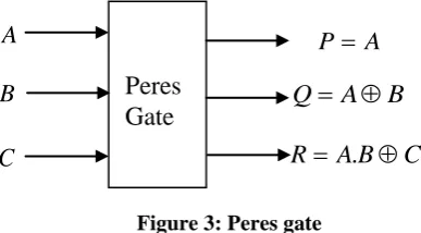
Figure 3: Peres gate
Several 4x4 and 5x5 gates have been described in the literature targeting low cost and delay which may be implemented in a programmable manner to produce a high number of logical calculations. The HNG gate, presented in [10], produces the following logical output calculations:
P
A
(1)
Q
B
(2)
R
A
B
C
(3)
S
(
A
B
).
C
(
AB
D
)
(4)The quantum cost and delay of the HNG is 6. When D = 0, the logical calculations produced on the R and S outputs are the required sum and carry-out operations for a full adder. The quantum representation of the HNG is presented in Fig. 4.
A
P
FG
A
B
Q
A
B
AC
B
A
Q
1
C
B
A
AB
C
A
R
1
FRG
A
P
B
A
Q
C
B
A
C
B
A
R
.
Peres
Gate
Figure 4: Quantum Representation of the HNG Gate
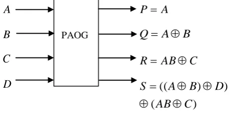
A new programmable 4x4 reversible logic structure - Peres And-Or (PAOG) gate – is presented which produces outputs
P
A
(5)
Q
A
B
(6)
R
AB
C
(7)
S
(
AB
C
).
C
((
A
B
)
D
)
(8)Fig. 5 shows the block diagram of the PAOG gate. This gate is an extension of the Peres gate for ALU realization.
Figure 5: Block Diagram of the PAOG
The ALU utilizes the PAOG gate and HNG gate to produce six logical calculations: ADD, SUB, AND, NAND, OR and NOR. The cost and delay calculations are identical to the ALU in table 2. The proposed ALU is shown in Fig. 6, and the logical results based on the input opcodes are presented in Table 1.
Table 1: ALU Opcodes and Logical Result for Proposed Design
S4 S3 S2 S1 S0 RESULT
0 0 0 0 0 AND
0 0 0 1 0 NAND
1 0 0 0 0 OR
0 1 1 0 0 NOR
1 1 0 0 ADD
1 0 0 0 0 SUB
A
P
B
A
Q
C
AB
R
)
(
)
)
((
C
AB
D
B
A
S
A
B
C
D
PAOG
A
B
C
D
V
V
V
V+
+
P
Q
R
Figure 6: Proposed Design, where
Q
A
B
III.
LITERATURE
SURVEY
The research on reversible logic is being pursued towards both design and synthesis. In the synthesis of reversible logic circuits there have been several interesting attempts in the literature such as the work in [4-8]. The ALU had five fixed select lines, and produced the following logical outputs: ADD, SUB, NSUB, XOR and NOP. The least significant bit comprised of two Feynman gates and two Toffoli gates. Each additional bit also had two Fredkin gates.
Matthew Morrison et al. [4], Design of a Reversible ALU based on Novel Programmable Reversible Logic Gate Structures. Reversible logic is widely being considered as the potential logic design style for implementation in modern nanotechnology and quantum computing with minimal impact on physical entropy. Recent advances in reversible logic allow for improved quantum computer algorithms and schemes for corresponding computer architectures. Significant contributions have been made in the literature towards the design of reversible logic gate structures and arithmetic units, however, there are not many efforts directed towards the design of reversible ALUs. In this paper, we propose the design of two programmable reversible logic gate structures targeted at ALU implementation and their use in the realization of an efficient reversible ALU is demonstrated. The proposed ALU design is verified and its advantages over the only existing ALU design are quantitatively analyzed. The overall delay and cost of this paper is 4n+7 and 26n-2 respectively. For 32bit delay and cost of this paper is 135 nsec and 830 respectively
Saurabh Kotiyal et al. [5], the two new reversible passages ORG-I and ORG- II are proposed as they can execute a reversible snake with decreased optical cost which is the measure of number of Mzis switches and the spread deferral, and with zero overhead in regards to number of ancilla inputs and the waste yields. The proposed all optical reversible snake diagram concentrated around the ORG-I and ORG-II reversible entryways are stood out and showed from be better than the following existing diagrams of reversible snake proposed in non-optical space with respect to number of Mzis, deferral, number of ancilla inputs and the refuse yields. The proposed all optical reversible swell pass on snake will be a key section of an all optical reversible ALU that could be joined in a wide blended sack of optical marker get ready demands. The overall delay and cost of this paper is 3n+1 nsec and 6n+1 respectively. For 32bit delay and cost of this paper is 97 nsec and 192 respectively
quantum computing and nanotechnology. In this paper we propose a novel 4x4 bit reversible multiplier circuit. The proposed reversible multiplier is faster and has lower hardware complexity compared to the existing counterparts. It is also better than the existing counterparts in term of number of gates, garbage outputs and constant inputs. Haghparast and Navi recently proposed a 4x4 reversible gate called "HNG". The reversible HNG gate can work singly as a reversible full adder. In this paper we use HNG gates to construct the reversible multiplier circuit. The proposed reversible multiplier circuit using HNG gate can multiply two 4-bits binary numbers. The proposed reversible 4x4 multiplier circuit can be generalized for NxN bit multiplication. We can use it to construct more complex systems in nanotechnology. . The overall delay and cost of this paper is 15n-10 and 22n-10 respectively. For 32bit delay and cost of this paper is 470 nsec and 694 respectively
Morrison, M. et al. Design of a novel reversible ALU using an enhanced carry look- ahead adder” Nanotechnology (IEEE-NANO), 2011 11th IEEE Conference Reversible logic is gaining significant consideration as the potential logic design style for implementation in modern nanotechnology and quantum computing with minimal impact on physical entropy. Recent advances in reversible logic allow schemes for computer architectures using improved quantum computer algorithms. Significant contributions have been made in the literature towards the design of reversible logic gate structures and arithmetic units, however, there are not many efforts directed towards the design of reversible ALUs. In this work, a novel programmable reversible logic gate is presented and verified, and its implementation in the design of a reversible Arithmetic Logic Unit is demonstrated. Then, reversible implementations of ripple-carry, carry-select and Kogge-Stone carry look-ahead adders are analyzed and compared. Next, implementations of the Kogge-Stone adder with sparsity-4, 8 and 16 were designed, verified and compared. The enhanced sparsity-4 Kogge-Stone adder with ripple-carry adders was selected as the best design, and its implemented in the design of a 32-bit arithmetic logic unit is demonstrated.
IV.
CONCLUSION
The 4bit reversible ALU is designed by integrating various sub modules that includes adder/subtract or, and logical unit. The logical unit performs AND, OR, NOR, XOR, NAND. The performance evaluation of the various sub modules are carried out using Modalism 6.5 tools and it was found that the circuits designed using reversible logic showed a reduced delay and power. As a future work more arithmetic and logical function can be used.
REFERENCES
[1]. A. Peres, Reversible logic and quantum computers, Phys. Rev. A 32 (1985) 3266–3276.
[2]. E. Fredkin and T. Toffoli,”Conservative Logic”, Int‟l J. Theoretical Physics Vol 21, pp.219-253, 1982.
[3]. R Feynman “ Quantum Mechanical Computers”, Optical News, Vol.11, pp 11-20, 1985
[4]. Matthew Morrison and Nagarajan Ranganathan2013” Design of a Reversible ALU based on Novel Programmable Reversible Logic Gate Structures
[5]. Saurabh Kotiyal, Himanshu Thapliyal and Nagarajan Ranganathan, “Mach-Zehnder Interferometer Based Design of All Optical Reversible Binary Adder” 2012 IEEE.
[6]. Matthew Morrison, Matthew Lewandowski, Richard Meana and Nagarajan Ranganathan, “Design of a Novel Reversible ALU using an Enhanced Carry Look- Ahead Adder” , 2011 11th IEEE International Conference on Nanotechnology Portland Marriott August 15-18, 2011, Portland, Oregon, USA. [7]. Rakshith Saligram Shrihari Shridhar Hegde1 Shashidhar A Kulkarni1 H.R.Bhagyalakshmi1 and
M.K. Venkatesha „DESIGN OF PARITY PRESERVING LOGIC BASED FAULT TOLERANT REVERSIBLE ARITHMETIC LOGIC UNIT „
[8]. Prashant .R.Yelekar (M.Tech) YCCE, Nagpur2011 Introduction to Reversible Logic Gates & its Application