Abstract—Two stage (Miller) opamp is one of the most commonly used opamp architectures in analog and mixed signal design. This paper presents the design of a Miller opamp using Potential Distribution Methodology (PDM). It is observed that a wide variety of design objectives depend on distribution of voltages and currents across the differential and gain stage. These dependencies are exploited to optimize the opamp performance and simulation results are presented.
Index Terms—CMOS, opamp, PDM.
I. INTRODUCTION
Analog and mixed signal design has always been a challenging task. Opamps are one of the most important building blocks of analog and mixed signal circuits. Typical opamp design techniques given in literature [1], [2], [3] and even recently published work [4], [5] concentrate mainly on analytical design approach. Being based on SPICE level 1 or level 2 models, the mathematical expressions associated with these techniques are generally simple. However, these expressions are large in number. Young and novice designers may find it difficult to manage so many equations. Alternate design methodologies are also proposed in [6], [7], which handle these equations using other tools like MATLAB, Mathematica, etc. Managing equations may become easier with these tools; however, the design methodology may become extremely complex. When the results obtained by these techniques are used to implement circuits in modern simulator using deep sub-micron devices (which is usually the case), the simulation results do not match with mathematical expectations. This is primarily due to the fact that deep sub-micron devices are modeled using long channel equations. The designer is then forced to adopt a simulator-based approach to optimize the design. Whatever may be the approach; the net time to market increases significantly. PDM is an analog design methodology, which is free from any analytical expression. It directly uses the simulator to arrive to a design point. As the simulator uses the target technology and is capable of handling accurate and complex SPICE models like BSIM, unexpected results or
Manuscript received June 22, 2012; revised July 29, 2012. This work was supported in part by National Institute of Technology, Durgapur under Grant SMDP.
Ashis Kumar Mal and Rishi Todani are with the National Institute of Technology, Durgapur India (e-mail: [email protected], [email protected]).
Abirjyoti Mondal was with the National Institute of Technology, Durgapur INDIA. He is now with the Department of Computer Engineering, Malaviya National Institute of Technology, Jaipur, India (e-mail: [email protected]).
Om Prakash Hari is with the Tejas Netwoks Ltd. (e-mail: [email protected]).
response is avoided.
In PDM, the dimensions of a device are found using a simulator; such that a desired current at pre-defined bias conditions are set. Since the bias conditions are predefined, PDM ensures that all the transistors are in saturation. This methodology can be applied to any analog block and is independent of power supply and technology. In this work, a 2-Stage opamp is designed using PDM. The performance of an opamp is characterized by a number of metrics such as gain bandwidth, phase margin, slew rate, low frequency gain and output swing. These performance metrics are determined by bias currents, component parameters, etc. Further, since opamps are often employed with negative feedback [8], frequency compensation becomes vital for closed loop stability. In order to achieve the required degree of stability, usually indicated by phase margin, other performance parameters are compromised. The following section presents the design approach, simulation results and design optimization techniques.
Fig. 1. Schematic of 2-stage miller opamp.
II. SINGLE-ENDED 2-STAGE OPAMP ARCHITECTURE
Fig. 1 details the architecture of a 2-Stage Miller opamp [8], [9]. The circuit consists of an input differential stage and a common source stage. A compensation capacitor (CC)
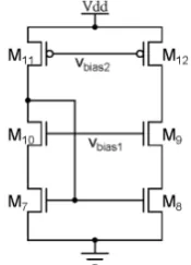
provides negative feedback to common source amplifier. Wide Swing Current Mirror shown in Fig. 2, and given in [1], [10], biases the differential and gain stage. This opamp is widely used in a variety of applications such as switched capacitor filters, sensing circuit, analog to digital converters.
Fig. 2. Schematic of wide swing current mirror
Simulator Based Simplified Design Approach of a CMOS
2-Stage Opamp
III. DESIGN OF 2-STAGE OPAMPUSING PDM The 2-Stage opamp is initially designed without much consideration on its performance metrics. Once, the first version of the design is ready, it is modified and optimized to meet the design requirements. PDM uses simulator to find the device dimensions that causes a specified current at pre-defined bias conditions. The bias conditions are chosen such that
V
DS≥
V
GS−
V
T keepingV
GS≥
V
T . Using theseconditions, the bias voltages are selected ensuring that the devices remain in saturation. In this work, proprietary 180 nm CMOS process employing BSIM 3v3 model has been used with VDD = 1.8V. The lengths of all transistors are fixed
at 500 nm. The design methodology is broken into following steps:
A. Identify Node Voltages
It is desirable to note all the node voltages that are at common mode level (in this case
V
DD/
2
or approximately0.9 V). It is identified that the input nodes (
v
in+ andv
in−)and the output node (
V
out) must be kept atV
DD/
2
.B. Tail Current, ITail
Slew rate (SR) requirement sets the lower limit of tail current (
I
Tail) and is given byL Tail
SR
C
I
=
×
where
C
Lis the load capacitance. Half of this tail current(
I
Tail/
2
) flows through the differential pair transistors,0
M
&M
1. Current mirror shown in Fig. 2 biasesM
2which sets
I
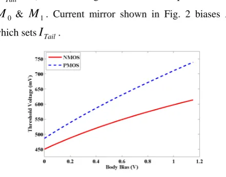
Tail.Fig. 3. Effect of body bias on threshold voltage.
C. Threshold Voltage Estimation
It is known that stacking of transistors lead to body bias, which in turn increases threshold voltage of the devices. For proprietary 180nm CMOS process, the effect of body bias on threshold voltage is shown in Fig. 3.
D. Tail Transistor, M2
The design is started by estimating drop across tail transistor (M2). It does not experience any body bias and
carries a current equal to ITail. From Fig. 3 its threshold
voltage (VT0n) is read as 0.45 V. With overdrive (Vov) of 0.1
V, an appropriate bias voltage of
vb
1
=
0
.
55
Vis applied to gate. Drain to source drop across tail transistor is kept at 0.3V. Thus node A is kept at 0.3 V. Thus, for M2,
55
.
0
=
GS
V
V andV
DS=
0
.
3
V. Using simulator a plot of drain current versus transistor width at pre-defined bias conditions is obtained. From this plot, the transistor width corresponding to ITail is chosen.E. Differential Pair M0 and M1
From Fig. 1 it is noted that gates of M0 and M1 are at
2
/
DDCM
V
V
=
. The source terminal (node A) of these transistors is at 0.3V. Thus the differential pair will haveV
GS=
0
.
6
V. Due to existence of body bias, thresholdvoltage (VTn) of M0 and M1 is more than VT0n. VTn of M0 and
M1 must be less than VGS with body bias. If not, then the
potential at node A is changed accordingly so as to lower body bias and threshold voltage. Since differential pair is fully symmetric between differential inputs, transistor sizes are also fully symmetric. To keep M1 in saturation, voltage at
node B is kept at 0.8 V. Due to systematic offset condition, drain voltage of M0 is same as that of M1. Thus for
differential pair,
V
GS=
0
.
6
V andV
DS=
0
.
5
V. Therefore,B and C are at 0.8 V.
F. Current Mirror M3 and M4
Transistor
M
3 is always in saturation becauseV
GD=
0
.Systematic offset condition implies that drain source (VDS)
voltage of M4 is same as that of M3. So M3 is also in
saturation. Dimensions of M3 and M4 are noted for
predefined bias voltages using simulator.
G. Transistor M5 and M6
The voltage at node B is applied to gate of NMOS driver (M5) and an appropriate voltage of 0.6 V to gate of PMOS
load (M6). The output of opamp is fixed at 0.9 V. It is noted
that with above set up M5 and M6 are in saturation. The
dimensions of M5 and M6 are obtained using simulator for a
current same as
I
Tail.H. Compensation Network
Compensation capacitor (CC) is included in the negative
feedback path of the second stage. Its function is to enhance the Miller effect already present in M5, and thus provide the
opamp with a dominant pole. The value of CC is selected
using
0.22
c L
c
=
×
c
Typically, 2-Stage opamps employ a compensation resistor in series with the compensation capacitor to place a zero on the negative real axis. As per the available literature, the value of this resistor is given by:
5
1
m
R
G
≥
where, Gm5 is the transconductance of the second stage. The
(TG). Using TG instead of a resistor makes the design area efficient. Test circuit shown in Fig. 4. is used to estimate the resistance offered by TG. Care is taken that the transistors are operating in linear or triode region and a plot of device dimension versus resistance is obtained as shown in Fig. 5. From this, suitable device dimension is chosen which offers required resistance. When all the device dimensions are found out, the complete opamp schematic is drawn and simulated.
Fig. 4. Test circuit for estimation of resistance using TG.
Fig. 5. Plot of resistance versus dimensions.
TABLE I: NODE POTENTIALS AT INITIAL DESIGN
Node Potentials A 0.3 B 0.8 C 0.8
v
in+ 0.9
v
in− 0.9
v
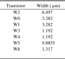
out 0.9TABLE II: TRANSISTOR WIDTH AT INITIAL DESIGN (L=500NM)
Transistor Width ( µm) W2 6.497 W0 3.282 W1 3.282 W3 1.192 W4 1.192 W5 0.8855
W6 1.317
IV. SIMULATION RESULTS AND ANALYSIS
Using the design steps discussed in previous section, a 2-Stage Miller opamp was designed using 180 nm CMOS process employing Cadence Spectre. The current in the tail
transistor (M2) of differential stage was kept at 30 µA. The
node potentials at the initial design set up are shown in Table I. The current in the gain stage was fixed at ITail. Dc analysis
results show that all transistors are in saturation and respective dimensions are noted as shown in Table II. AC
analysis results with
C
L=
1
pF andC
C=
220
fF isshown in Table III.
TABLE III: INITIAL RESPONSES
Performances Response
Gain 60.3 dB
Bandwidth 107.6 kHz Phase margin 62º UGF 86.41 MHz
V. OPTIMIZATION
The effect of current and voltage distribution across the opamp is now examined. It is found that the performance of the opamp can be optimized in two ways. First, the current distribution between the differential and gain stage, and second, adjusting the potential at nodes A and B.
A. Current Distribution
Keeping the node voltages fixed at pre-defined values shown in Table I, currents in M2 and gain stages are varied in
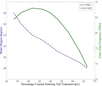
such a way so that total current remains same. Again dc analysis followed by ac analysis is performed for specified current branching. The transistor dimensions are noted along with performance metrics for the same capacitance value. Fig. 6 depicts dependency of DC gain and 3 dB bandwidth (BW) on percentage current entering differential transistors. It is seen that DC gain remains constant whereas BW improves with current branching. Fig. 7 shows the variation of phase margin (PM) and unity gain frequency (UGF) with current branching. Both PM and UGF are decreasing with percentage current entering differential pair. Taking the stability of the opamp into consideration, a suitable current distribution which sets the desired PM may be chosen.
Fig. 7. Phase margin and unity gain frequency dependency.
B. Node Voltage Variation
Further analysis was performed with currents from previous results. Here current is kept fixed at both tail transistor and gain stage while node voltages are varied. The voltages at either of the nodes A or B are varied keeping the other at fixed value. The selection of voltages is done taking into consideration threshold voltage of the transistors and gate bias voltages. After one iteration of analysis, the potential at fixed node is changed to next suitable value. It is kept fixed and variation occurs at other node for the said current only.
C. Potential at Node A
Initially current in M2 and gain stage was fixed at 30 µA.
The voltage at node B was fixed at 0.8 V and node A voltage was varied. Then dc analysis followed by ac analysis is performed for every possible voltage distributions. Transistor dimensions are noted using simulator. Performances are first noted for
C
L=
1
pF andC
C=
220
fF.Fig. 8. Gain and 3dB bandwidth dependency.
Fig. 9. Phase margin and unity gain frequency dependency.
Then the improved performances are obtained with
400
=
LC
fF andC
C=
88
fF [1]. This process is repeated by specifying a fixed voltage at node B and simultaneously varying node A voltage for same pre-defined current. From Fig. 8-9 it is noted that gain, BW and UGF improves while PM lowers for fixed voltage at node B and variation at node A.D. Potential at Node B
Now the potential at node A is kept fixed and potential at nodes B is varied. Performances are first noted for default value of capacitances and then improved performances for pre-defined value of capacitances. Fig. 10-11 depicts that gain, PM and UGF are lowering while BW improves for fixed voltage at node A and variation at node B. Although PM is diminishing it is within the limit for a specific voltage distribution mentioned initially so as to attain stability. The optimal results are obtained when drop across the tail transistor is kept at 300 mV, drop across differential pair is around 700 mV and rest drop across PMOS load. It was also observed that same trend in changes occur for the remaining current branching.
Fig. 10. Gain and 3dB bandwidth dependency.
Fig. 11. Phase margin and unity gain frequency dependency
TABLEIV:PERFORMANCE MEASURES FOR 30 µAIN TAIL PORTION AND NODES A AND B AT 300 MV AND 700 MV RESPECTIVELY
Performances Initial Performance Optimized
Gain 60 dB 62 dB
Bandwidth 107.6 kHz 240 kHz
Phase margin 62º 59º
UGF 86.41 MHz 237 MHz
VI. CONCLUSION
PDM is found to be free from complexity of analytical expressions and maintains a simple design methodology, which can be applied to any analog design. So novice designers can implement the steps mentioned previously to design an opamp. Since PDM is independent of supply voltage, process technology and the MOSFET model being used, it can be applied to any complex opamp structures. The results are obtained quickly and are accurate to a greater extent as compared to designs based on analytical equations. The Potential Distribution Method (PDM) proposed earlier is repeated here for the design of 2-Stage Miller opamp and the trade off associated with tail current variations upon performance metric was plotted. It is observed that a specific voltage distribution using PDM results in improved performances and the transistors in saturation, thus simplifying the design process.
ACKNOWLEDGMENT
The authors gracefully acknowledge Dr. Debashis Datta, Ministry of Communication and Information Technology, Govt. of India, for extending the SMDP project at NIT Durgapur. Prof. S. K. Datta, Prof. G. K. Mahanti SMDP chair of NIT Durgapur and Prof. Swapna Banerjee, SMDP chair of IIT Kharagpur are thanked. The authors also acknowledge Kanchan Maji, Project Engineer SMDP II, for his kind assistance.
REFERENCES
[1] P. E. Allen and D. R. Holberg, CMOS Analog Circuit Design, Oxford University Press, 2007.
[2] B. Razavi, Design of Analog CMOS Integrated Circuits, Analysis and Design, Tata McGraw-Hill Publishing Company Limited, 2002. [3] S. Franco, Design with Operational Amplifiers and Analog Integrated
Circuits, McGraw-Hill Companies, 1997.
[4] P. K. Meduri and S. K. Dhali, “A framework for automatic OpAmp sizing,” IEEE International Midwest Symposium on Circuits and Systems, pp. 608-611, Aug. 2010.
[5] K. Bult and G. Geelen, “A Fast-Settling CMOS Operational Amplifier for SC circuits with 90-dB DC Gain,” IEEE J. of Solid-State Circuits, vol. 25, pp. 1379–1384, Dec. 1990.
[6] P. Mandal and V. Visvanathan, “CMOS Op-Amp Sizing Using a Geometric Programming Formulation,” IEEE Trans. on Computer
Aided Design of Integrated Circuits and Systems, vol. 20, no. 1, pp. 22-38, Jan. 2001.
[7] M. Hershenson, S. Boyd, and T. Lee, “Optimal Design of a CMOS Op-amp via Geometric Programming”, IEEE Transactions on Computer-Aided Design, vol. 20, no. 1, pp. 1-21, Jan. 2001.
[8] P. R. Gray and R. G. Meyer, “MOS Operational Amplifier Design—A Tutorial Overview,” IEEE J. of Solid-State Circuits, vol. 17, pp. 969–982, Dec. 1982.
[9] D. A. Johns and K. Martin, Analog Integrated Circuit Design, New York: Wiley, 1997.
[10] R. J. Baker, CMOS Circuit Design, Layout, and Simulation, Wiley-Interscience, 2005.
Ashis Kumar Mal received his Ph.D. in
microelectronics and VLSI from the Indian Institute of Technology, Kharagpur, India, in 2009. He joined the Electronics and Communication Engineering Department, North Eastern Regional Institute of Science and Technology (NERIST), Itanagar, in 1993 as a Lecturer. In 2007, he joined the National Institute of Technology (NIT), Durgapur, and currently serves as an Associate Professor there. His research interests include mixed signal VLSI design, sampled analog circuits, interconnect modeling, and optical networking. He has coauthored more than 40 technical papers. He is a member of IEEE.
Abir jyoti Mondal was born in June 1984, India. He
did his Bachelor of Engineering in Electronics and Communication engineering under Burdwan University, India in 2007. Further he completed his M.Tech degree in Microelectronics and VLSI from National Institute of Technology, Durgapur, India in 2011. His major field of study is Networks on Chip. He is currently working as a Research Scholar at Malaviya National Institute of Technology, Jaipur, India.
Om Prakash Hari obtained his B. Tech in Electronics
& Communication Engineering, from The Techno School, Bhubaneswar, under Biju Patnaik University of Technology, Rourkela, India in 2009. He received M. Tech degree in Microelectronics & VLSI under department of Electronics and Communication Engineering, from National Institute of Technology, Durgapur, India, in 2011. His current research activities and interest include VLSI system design, high speed ADCs, high speed serial protocol design, semiconductor memories design and optimization. He is currently working as Research & Development Engineer at Tejas Networks Ltd, Bangalore, India.
Rishi Todani was born in a small town called
Raniganj, situated in the Burdwan district of West Bengal, India, on 3rd October 1985. He obtained his