97010-0404 IJET-IJENS © Decem ber 2009 IJENS
Abstract— The optimization of 45nm NMOS device was
studied using Taguchi Method. This method was used to analyze the experimental data in order to get the optimum results. In this paper, there are four factors were varied for 3 levels to perform 9 experiments. S ilicide on the poly-S i gate electrode was used to reduce the gate electrode resistance. The virtually fabrication of 45nm NMOS device was performed by using ATHENA module. While the electrical characterization of device was implemented by using ATLAS module. The values of oxide and silicide thickness after optimization approach were 1.52709nm and 25.26nm respectively. The result of the threshold voltage (VTH) is 0.148468 Volts. In this research,
silicide thickness and oxide thickness are the main factors were identified as the source of the inability of the trans istors to perform. The oxide thickness also was identified as one of the factors that has the strongest effect on the response characteristics.
Index Term-- Optimization of 45nm nMOS , Cobalt S ilicide,
Taguchi Method
I. INT RODUCT ION
The scaling of the Complementary Metal Oxide Semiconductor (CMOS) devices to smaller physical dimensions has became the driving force for the semiconductor industry to meet the market’s demand for greater functionality and performance of the integrated circuit at a low cost [1]. This was the primary activity of advanced device development almost since the basic technology was established. By reducing the device dimensions of the integrated circuits, the device performance can be greatly improved in terms of switch speed [2]. Meantime, the manufacturing cost of each device can also be reduced by decreasing the device dimensions. The reduction of CMOS source/drain depth is important for suppressing MOS punch through leakage and minimize device short channel effect such as drain-induced barrier lowering (DIBL) in submicron CMOS devices [3,4]. In order to minimize short channel effects (SCE) and maximize device performance simultaneously, an advanced source/drain engineering associated with diffusion profiles of source and drain junction should explored for the optimum CMOS device design. The self-aligned silicide (SALICIDE) technology has been widely
use to reduce res istance of polysilicon gates [5]. This is because the sheet resistance will be the major limiting factor of the device performance [6]. The use of metal silicide in integrated circuits as a contact material has been widely researched. This metal reacts with polysilicon to form the metal silicide layer that posses better physical and electrical properties to interface with aluminium [7]. Since the metals with low work functions are inherently unstable and reactive, searching for a suitable metal for the n-Metal Oxide Semiconductor Field Effect Transis tor (n-MOSFET) gate electrode with thermal stability compatible with CMOS front end processes are a challenge. Recently, metal silicide such as Cobalt Silicide
(CoSi
2) for dual metal gates has drawn considerable attention due to their CMOS compatibility an d no process-induced damage to the gate dielectric. Because of the ease of formation in small dimensions, cobalt silicide has matured into an important alternative to titanium silicide for contacts to silicon in CMOS devices.SILVACO ATHENA module is an example of a TCAD tool that can be manipulated effectively in studying the downscaling process. It would give the economical and speed edge to the traditional way of doing things [8]. Semiconductor TCAD tools are computer programs, which allow for the creation, fabrication and simulation of semiconductor devices. These simulations provided the opportunity to study the effect of different device parameters on the overall device performance [9]. All the device modelling need to do optimizations approach to get optimum performance for CMOS technology. The optimization of manufacturing operations and products is one of the vital industrial functions to improve the product performance as well as to save manufacturing cost. A systematic and efficient way to achieve this is to use an optimization method of designing experiments based on Taguchi Methods. Taguchi Methods provide the most efficient and viable solution in such cases with minimal experimental trials [10].
II. MAT ERIAL AND MET HODS
Sample used in these experiment were <100> orienting and p-type (boron doped) silicon wafers. P-well was created starting with developing a 200Å oxide screen on the top of the wafer followed by boron doping. The oxide layer was etched after the doping process was completed. It was followed by annealing
Fauziyah Salehuddin
1, Ibrahim Ahmad
1, Fazrena Azlee Hamid
1, Azami Zaharim
2,
College of Engineering Universiti Tenaga Nasional (UNITEN)1
43009 Kajang, Selangor, MALAYSIA, Universiti Kebangsaan Malaysia (UKM)2,
Application of Taguchi Method in Optimization
of Gate Oxide and Silicide Thickness for
process to strengthen the structure. Next, STI was developed to isolate neighbouring transistor. A 130Å stress buffer was developed on the wafers with 25-minute diffusion processes. Then, a 1500Å nitride layer was deposited using the Low Pressure Chemical Vapour Deposition (LPCVD) process. This thin nitride layer will be acted as the mask when silicon was etched to expose the STI area. Photo resistor layer was then deposited on the wafers and unnecessary part will be removed using the Reactive Ion Etching (RIE) process. An oxide layer was developed on the trench sides to eliminate any items from entering the silicon substrate. Chemical Mechanical polishing (CMP) was then applied to eliminate extra oxide on the wafers. Lastly, STI was annealed for 15 minutes at 900oC temperature. A sacrificial oxide layer was then developed and etched to eliminate defects on the surface.
The gate oxide was laid down and a Boron Difluoride (BF2) threshold-adjustment implant was done in the channel region through this oxide. The polysilicon gate was then laid and defined followed by the halo implantation. In order to get an optimum performance for NMOS devices, indium was doped. Halo implantation was followed by developing sidewall spacers. Sidewall spacers were then used as a mask for source/drain implantation. An arsenic atom was implanted at a desired concentration to ensure the smooth current flow in NMOS.
Silicide layer was then grown on the top of polysilicon. The next step in this process was the development of Boron Phosphor Silicate Glass (BPSG) layer. This layer will be acted as Premetal Dielectric (PMD), which is the first layer deposited on the wafer surface when a transistor was produced. This transistor was then connected with aluminum metal. After this process, the second aluminum layer was deposited on the top of the Intel Metal Dielectric (IMD) and unneeded aluminum was etched to develop the contacts [8]. The procedure was completed after the metallization and etching were performed for the electrode formation and the bonding pads were opened. Once the devices were built with ATHENA, the complete devices can be simulated in ATLAS to provide specific characteristics such as the ID versus VGS curve. The threshold voltage (VTH) and the transconductance (gm) can be extracted from that curve [9].
A. Optimization Approach
Taguchi’s parameter design method is an important tool for robust design. The Taguchi method involves an analysis that reveals which of the factors are most effective in reaching the goals and the directions in which these factors should be adjusted to improve the results [10]. The optimization of the nMOS devices have been done by changing individual process parameters laid out by the ATHENA [9].
For perform the experiment to finding the optimum solutions of silicide thickness and oxide thickness in 45nm NMOS transistor, all the factors were varied for 3 levels to form L9 orthogonal array [10];
Silicide Diffusion Time Level 1 - 0.005 seconds Level 2 - 0.0075 seconds
Level 3 - 0.01 seconds
Silicide Anneal Temperature Level 1 - 910oC
Level 2 - 930oC Level 3 - 940oC
Oxide Anneal Temperature Level 1 – 847oC Level 2 – 845oC Level 3 – 850oC
The variations are being applied to the L9 orthogonal array for Taguchi Method analysis.
III. RESULT ANDANALYSIS
The fabrication result of the first set experiment that was virtually fabricated using ATHENA module was discussed. The results of VTH, RS and IOFF were then analyzed and processed with Taguchi Method Analysis.
A. 45nm pMOS Transistor Fabrication
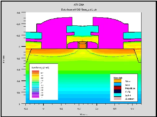
Fig. 1 shows clearly on the doping concentration across the 45nm nMOS transistor. The fig. shows the tabulation of silicon, silicon dioxide, polysilicon, silicon nitride, cobalt silicide and aluminum. Doping concentration is the main factor that will determine the electrical performance of the transistor. A good doping concentration will ensure the transist or works well with enhance gate control and less leakage current. The doping concentration comes from source/drain doping process that is supposedly to control the threshold voltage value [9]. The values of oxide thickness and gate length for the device are 1.52678nm and 35nm respectively.
Fig. 1. 45nm nMOS T ransistor Doping Concentration
97010-0404 IJET-IJENS © Decem ber 2009 IJENS silicide thickness or oxide thickness, the transistor can be
improved [8].
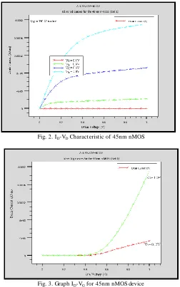
Fig. 2. ID-VD Characteristic of 45nm nMOS
Fig. 3. Graph ID-VG for 45nm nMOS device
Fig. 4. MOSFET sub-threshold ID-VG for 45nm nMOS device
Fig. 5 shows that the average of silicide thickness for NMOS device is 25.26nm. We can see clearly that the shape is not uniformed. Its shape like an amour with two sharp end. This is
caused by the natural way that cobalt diffuse into polysilicon [9].
Fig. 5. Silicide Structure.
B. Analysis of the Factors Effect to the Threshold Voltage for 45nm
Table I show that the results of VTH, RS and ION were tabulated for NMOS device. Each of these results was subjected to Taguchi Method and the outcomes of the analysis were shown in Table II and Table III.
TABLE I
VTH, Rs and Ion values from the simulations
Threshold voltage (VTH) is the main reason for a capacitor to work or not. Sheet resistance will define the maximum speed of the transistor to turn-on. Although this is not as important as VTH it will be useful for high speed device [8]. In Taguchi designs, the magnitude of the factor coefficient usually mirrors the factor rank in the response table. The factor with the highest coefficient is ranked 1 in the response table.
Table II and Table III show that the results of the data indicate that;
For the means, factor 3 also has the strongest effect on the response because it has the biggest coefficient (-0.0053) if compared to the other factors.
TABLE II
Estimated Model Coefficients for SN ratios
Factor Coefficient T-value P-value
1 -0.0000 -0.631 0.593
2 -0.0003 -8.632 0.013
3 0.0012 33.122 0.001
S= 0.00007986 R-Sq=100.0% R-Sq(adj)=100.0%
TABLE III
Estimated Model Coefficients for Means
Factor Coefficient T-value P-value
1 0.0004 1.995 0.184
2 0.0017 9.871 0.010
3 -0.0053 -29.734 0.001
S= 0.0003760 R-Sq=100.0% R-Sq(adj)=100.0%
Table IV and Table V show the p-value in the analysis of variance table for determine which of the factors in the model are statistically significant. The results of the data indicate that;
For the SN ratios, the p-values indicate that all of the factors are significant at the 0.05 -level.
For the means, the p-values also indicate that all of the factors are significant at the 0.05 -level.
TABLE IV
Analysis of Variance for SN ratios
Factor DF Seq SS F-Ratio P-value
1 2 0.000001 60.93 0.016
2 2 0.000002 148.72 0.007
3 2 0.000833 65320.85 0.000
TABLE V
Analysis of Variance for Means
Factor DF Seq SS F-Ratio P-value
1 2 0.000021 74.56 0.013
2 2 0.000049 171.83 0.006
3 2 0.020946 74064.49 0.000
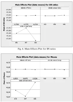
From the Sum of Square values, the result show, that oxide anneals temperature is the most dominant factor for determining the performance of the NMOS device. It can be seen from Fig. 6 and Fig. 7 where the slope of this factor is the steepest among the other factor. Main effect plots show how each factor affects the response characteristic. The greater the differences in the vertical position of the plotted points, the greater the magnitude of the main effect. This depicts the values of VTH, RS and ION will be changed with changing the oxide anneal temperature in comparison to the other factors.
Fig. 6. Main Effects Plot for SN ratios
Fig. 7. Main Effects Plot for Means
The optimized factors for NMOS device which had been suggested by Taguchi method are 5ms, 910oC and 845oC for silicide diffusion time, silicide anneal temperature and oxide anneal temperature respectively.
With all the information, it can be clearly said that oxide anneals temperature must be controlled more dominantly in order to get a working transistor. From the above parameters, a final simulation was performed to verify the accuracy of the Taguchi Method prediction. The results show that the threshold voltage (VTH) values is 0.148468V for NMOS device. The values are within 12.7% of Berkeley Technology Predictive Model (BPTM) and International Technology Roadmap for Semiconductor (ITRS) prediction [11]. This shows that Taguchi Method is useful tool for predict the optimum solution in finding the 45nm PMOS fabrication recipe with appropriate threshold voltage value. In this research, silicide and oxide thickness are the main factors were identified as the source of the inability of the transistors to perform. The values of oxide and silicide thickness after optimizations approach is 1.52709nm and 25.26nm respectively.
IV. CONCLUSION
97010-0404 IJET-IJENS © Decem ber 2009 IJENS VTH is the main response studied in this project as it the main
factor in determining whether a digital device works or not. Polysilicon sheet resistance should also be kept as low as possible to increase the speed of the device by shortening the time to accumulate charge in the channel for a transistor to turn-on. Taguchi Method is being applied to successfully predict the optimum solution in achieving the desired transistor.
ACKNOWLEDGEMENT
The authors would like to thanks to the Ministry of Higher Education (MOHE) for their financial support and the Universiti Teknikal Malaysia Melaka (UTeM) for the moral support throughout the project.
REFERENCES
[1] P.D.Agnello et. al., “Process Requirem ents fo Continued Scaling of CMOS- the need and prospects for atom ic level manipulation”, IBM J. Res. & Dev. 46, No. 2/3 (2002) [2] R.Arghavani et. al., “k/Metal Gates Prepare for
High-Volume Manufacturing”, Semiconductor International, Reed Elsevier Inc. (2007)
[3] C.M.Osburn et. al., “Vertically scaled MOSFET gate stacks and junctions: How far are we likely to go?”, IBM J. Res. & Dev. 46, No. 2/3, 299-300 (2002)
[4] Sung-Mo Kang, Yusuf Leblebici, “CMOS digital integrated circuit: analysis and design”, McGarw-Hill Higher Companies, Inc., 3th Edition (2003)
[5] Sung-Mo Kang, Yusuf Leblebici, (2003)“CMOS digital integrated circuit: analysis and design”, McGarw-Hill Higher Companies, Inc., 3th Edition.
[6] Hiroshi Iwai, Shun’ichiro Ohmi, (2002) “Silicon integrated circuit technology from past to future”, Microelectronic Reliability, 465-491
[7] Pushkar S. Ranade, (2002)“ Advanced Gate Materials and Processes for Sub-70nm CMOS T echnology”, PhD. T hesis, Department of Materials Science and Engineering, Univercity of California, Berkeley.
[8] Husam Ahmed Elgomati, “Characterizing Cobalt Silicide and Gate Dielectric Thickness in 65nm NMOS Device”, Master of Science T hesis, Universiti Kebangsaan Malaysia. (2007) [9] Ashok K.Goel et al., (1995)“Optimization of Device
Performance Using Semiconductor TCAD Tools”, Silvaco International, Product Description, Silvaco International.
http://www.silvaco.com/products/descriptions.
[10] Douglas C. Montgomery, “Design and Analysis of Experiments”, John Wiley & Sons Inc., 6th Edition (2005) [11] IT RS 2007 Report; http://www.itrs.net