e-ISSN: 2278-067X, p-ISSN: 2278-800X, www.ijerd.com
Volume 11, Issue 12 (December 2015), PP.68-75
Determining the Compatibility of Sintered Silver Die Attach in
Terms of Delamination Performance as Compared to Existing
High Lead Solder Types in a Semiconductor Power Package
Richard Q. Clemente
1, Blessie B. Basilia
1, 2Erik Nino Tolentino
1Mapúa Institute of Technology School of Graduate Studies, Muralla St. Intramuros Manila2Industrial Technology Development Institute, Bicutan Taguig City
Abstract:- A quick and simple method for determining thermo-mechanical compatibility of sintered Ag die attach is presented without assembling samples for moisture level sensitivity assessments. Material components of a power semiconductor package such as the die attach material (high lead or SnPb solder and sintered silver die attach) , copper lead frame, silicon die and epoxy mold compounds were isolated. Each components were studied individually by subjecting samples of SnPb, sintered Ag and epoxy mold compound to digital scanning calorimetry (DSC). The purpose is to be able to simulate thermal stimulus during manufacturing process. After the 1st heat treatment, a second heating step was employed on all components which additionally includes a copper lead frame and silicon die. The purpose of this step is to simulate customer reflow conditions during board mount. This step also derives the thermal graphs to determine the thermo-mechanical behavior of each constituent material from low to high temperature stimulus. The results suggests that sintered silver performs better compared to the SnPb die attach thermo-mechcanically. The reason lies in the processing of these materials, SnPb transitions from a solid to liquid state at temperatures above 187oC. Hence during board mount, SnPb die attach has a tendency not to maintain structural integrity and thus prone to delamination. Sinter Ag on the other hand does not necessitate melting during its process steps and therefore maintains its structural integrity. Furthermore since sintered silver does not require melting process, the thermo-mechanical profile compared to other component material deviates less as compared to the SnPb solder types.
Keywords:- Sintered Silver, Die Attach, Tin Lead Solders, Thermal Analysis, Digital Scanning Calorimetry
I.
INTRODUCTION
A semiconductor package protects the die from external stimulus that can affect the performance of the device thermally, mehcanically or chemically. The silicon die is housed on an outer covering or an encapsulant material called mold compound. A leadframe typically copper is used to connect the final device to the printed wiring board. To connect the silicon die into the leadframe a die attach material is used. There are 3 main functions of a die attach material. First is to attach the die into the lead frame. Second is to dissipate heat across the lead frame and third is to provide reliabile connection and not fluctuate electrical stimulus when the device is in operation [1]. Depending on the complexity, sometimes wirebonds connect the silicon die into the lead frame. Discrete semiconductor devices particularly of high power applications utilizes a clip which eliminates the use of the wire thus increasing the reliability performance by effectively dissipating heat and providing a robust connection on the die [2]. The reliability in terms of connection is compromised if the interface delaminate. This could cause catasthropic effects which may lead to device failures during use[3]. This can also result into thermo mechanical defects such as die or package cracks [4]. Figure 1a and 1b illustrates some failure mechanisms that can be rooted to incompatible thermal expansions.
Figure 1b: Die crack images rooted to CTE mismatch
In order to ensure the material compatibility, understanding the behavior prior assembly is necessary. This can be achieved by subjecting samples to individual thermal assements resulting into different temperature graphs. Oftentimes, the thermal processing during assembly process is not understood as well as its interaction that results into field failures and reliability problems. Mold compounds and die attach materials are composed of thermosets wherein a pre heat treatment is necessary to activate the flowability and processing [5]. On the otherhand the lead frame and silicon die does not require pre heat treatment since they are not polymeric materials. In order to determine material compatibilities digital scanning calorimetry (DSC) and thermo mechanical analyzers are utlitized. The DSC is utilized to provide pre heat treatment for the thermo setting materials and the thermomechanical analyzer mimics the heat exeperienced by the package during board mount or reflow process. Individual TMA graphs are produced and overlayed across each other to determine if the constituent materials are compatible toward each other. This is the reason why exhaustive research and experimentations are done on materials in order to understand both thermal and mechanical behaviors. Thermomechanical analyzers provides a necessary information such as Tg and CTE. The equipment is composed of a pedestal that heats the specimen of interest. TMA’s output data can be in a form of a temperature versus time graph that can be vital in understanding thermal and mechanical behavior of materials. When applied to semiconductor components, the information provides a powerful insight to visually determine if the interaction is probable to delaminate. Figure 2 illustrates a Pb reflow profile. The typical peak temperature of the graph for Pb solders is around 210oC to 215oC. The value for peak reflow temperature is derived from the fact that board manufacturers use this temperature to mount semiconductor devices on the PCB. Previous studies were implemented on delamination [6] using such methods. In this case, this paper focuses on the interaction of the sinter Ag die attach materials in relation to the components making up the power semiconductor package.
II.
METHODOLOGY
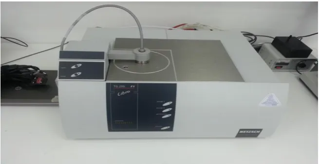
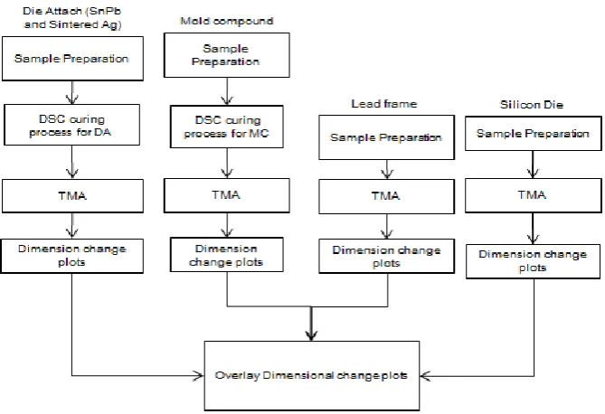
A Thermomechanical Analyser (TMA2940) and Digital Scanning Calorimetry (DSC 204 F1 Phoenix) were used to derive thermal graphs for components making up the semiconductor power package. Differential Scanning Calorimetry measures the heat flow in a material as a function of temperature and time. A sample is placed in a small Aluminium pan. Depending on the heating profile used, the tool can heat or cool a specimen. Nitrogen is employed in the process of heating and or cooling to ensure non-reactivity of the specimen [8]. DSC is effective in supplementing heating profiles for thermoset materials such as mold compounds and die attach materials.
TMA is used to characterize linear expansion, glass transitions, and softening points of materials by applying a constant force to a specimen while varying temperature. For expansion measurements, a probe rests on a sample on a stage with minimal downward pressure.
Sample preparation for sinter Ag die attach material, SnPb and epoxy mold compounds were thawed based on supplier recommendations. Table 1 shows the thawing time for these materials.
Material Thawing time (room temperature)
Epoxy Mold Compound 24 hours
Sinter Ag die attach 1.5 hours
High Pb Solder 4 hours
Table 1: Thawing conditions for mold compound, sintered Ag and SnPb solder.
After thawing, both sinter Ag and SnPb solder paste was placed in an aluminium pan. Powdered mold compound were prepared using a mortar and pestle; this is to ensure constant particle sizes. The thawed samples were eventually subjected to their required thermal profiles based on supplier recommendation.
Figure 3: DSC equipment to be used for the pre heating profiles of the mold Compound and die attach material
The following heat treatments were implemented:
Sinter Ag paste requires a thermal profile illustrated below 1.) Temperature ramp from 23oC to 150oC
2.) Followed by 150oC for 30 minutes 3.) Another ramp from 150oC to 250oC 4.) Followed by 250oC for 1.5 hours
5.) Cool down from 250oC to 27oC for 1 hour
High Pb solder paste requires a thermal profile illustrated below 1.) Initial ramp from 27oC to 150oC at 2.5oC /sec
The mold compound was cured from 185oC for 50s followed by a post mold cure step at 175oC for 3 hours. All material components that were subjected to DSC excluding the copper lead frame and the silicon die. Both samples were subjected to TMA along will all other components to determine the individual temperature profiles that will be superimposed.
Figure 4: TMA equipment to determine temperature profiles.
The materials were subjected to the same heating condition starting from room temperature until 300oC with a heat rate of 10oC/min. Full summary of the experimental procedures is illustrated in Figure 5.
Figure 5: Material Sample preparation methods in determining mechanical Thermographs of individual material components
III.
RESULTS
AND
DISCUSSION
Figure 6: Superimposed thermographs for material components making up the clip package.
Silicon Die and Copper Lead frame
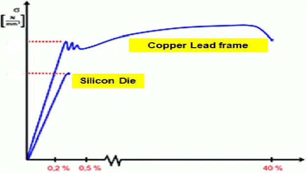
The silicon die and the lead frame material underwent a single heat treatment. The pre heat treatment is necessary for mold compound and die attach materials to activate polymeric components for the particles to agglomerate and thus enabling full mechanical stability of the semiconductor package. From the graph in figure 6, it is expected that the silicon die has minimal coefficient of thermal expansion with approximately 1/10 of a micron when heated from room temperature until 300oC at a heating rate of 10oC/sec. the findings here can be also related to the stress strain curves shown in figure 7 wherein the silicon die has lesser elastic limit and has the tendency to break instantly when it reaches a certain yield limit. For the copper lead frame, the curves extend to a regime after the yield stress wherein strain hardening and necking across the specimen is attained before fracture. This indicates that the copper lead frames can absorb and deform before it fractures. Contrary to the silicon die which break in an instant when the yield limit is reached.
Figure 7: Stress Strain Curves for the Silicon Die and Copper lead frame
High lead solder (SnPb) die attach
63%Pb and 37%Sn. The reason is that this combination yields the least melting temperature (eutectic) which is attractive for semiconductor manufacturing. From the SnPb phase diagram, the eutectic solder melts around 187oC. A temperature below 187oC maintains the solder’s solid phase while a temperature higher than this changes the solder from a solid to a liquid phase. The TMA curves behave as expected based from the phase diagram. It is observed that at low temperatures the solder has slight changes in size. This can be attributed to the flux evaporation that did not escape the pre heat treatment so a small change in dimension is reflected. Further heating at temperatures from 150oC onwards we observe an exponential increase in size due to the phase transition from solid to liquid. This is also in unison to the phase diagrams in figure 8.
Figure 8: High lead Solder (SnPb) Phase diagram [11]
Epoxy Molding Compounds
The epoxy molding compound underwent two pre heat treatments. The first pre heat was for the purpose of simulating assembly process and the second heat treatment was to simulate actual reflow conditions. The epoxy mold compounds are polymeric types which are classified as thermosets. The epoxy mold compound requires a thermal reaction to be able to form cross linking chains among other polymeric species. Once the required thermal stimulus is achieved the reaction is said to be irreversible meaning that the mold compound cannot be reformed, re-melted and reused [9]. This is contrary to another type of polymer which is called thermoplastics which can be reused and reformed. The curing step for the mold compound in this experiment includes 2 stages. The first step is subjecting the samples for 185oC for 50s. This is to complete thermal reaction among the additives of the mold compound. The next steps include a longer step called post mold cure. The profile used is 175oC for 3 hours. The purpose of this step is to be able to complete the agglomeration of polymeric species and achieve full crosslinking of polymeric chains.
Sinter Ag Die Attach
The second heat treatment was used to be able to understand board mounting behaviors at customer side. The thermo-mechanical graphs for sintered Ag are illustrated in Figure 6. It is observed that the graphs of sinter Ag and copper lead frame behaves in unison compared towards each other. Whereas the SnPb die attach has a high thermal expansion above 150oC. The low melting point of SnPb warrants the occurrences of delamination in the die attach interfaces. Contrary to Sinter Ag materials which do not involve melting process. Hence, the
Analysis of combined thermal graphs for the components of the clip power package
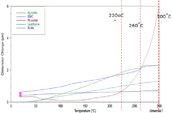
From the TMA graphs obtained we can now derive if the material is compatible at a specified temperature this is determined by drawing a line on the temperrature of interest. For instance, a temperature 220oC denotes the reflow profile for Pb containing solder alloys, 260oC denotes a typical reflow profiles for lead free. 3 temperature points were selected to see the compatibility of the following material sets. This is to determine if the new sinter Ag die attach material is performing better at this 3 temperature values. Figure 9 illustrates the TMA graphs with line markers. Table 2 summarizes the dimensional change values given the specific temperature. From table 2, we observe dimensional changes on various components. SnPb varies from 0.5um to 6um given this temperature values. This can pose delamination problems as this material expands abruptly. The sinter Ag material also varies however it was observed to be resistant to temperature changes compared to the current SnPb die attach material. Hence sinter Ag material could be an option for lead free packaging which could be resistant to delamination.
Figure 9: Temperature intercepted points at 220oC, 260oC and 300oC
Dimension Change (um)
at 220
oC
at 260
oC
at 300
oC
Ag sinter
1.8
2
2
Epoxy Mold Compounds
1
1.5
2
Pb solder
0.5
2
6
Leadframe
1.1
1.2
1.3
Si Die
1E-07
1E-07
1E-07
Table 2: Derived Dimensional Change for various materials for critical temperature range
IV.
CONCLUSIONS
ACKNOWLEDGMENT
The authors would like to express appreciation for the support of Dr. Jonathan W.L. Salvacion and Rosie Ann C. Pascual from the school of Graduate studies of the Mapua Institute of Technology. Also, the authors would like to extend their gratitude to the staff of ITDI and ADMATEL from the Department of Science and Technology.
REFERENCES
[1]. M. Knoerr, A. Schletz “Power Semiconductor Joining through Sintering of Silver Nanoparticles: Evaluation of Influence of Parameters Time, Temperature and Pressure on Density, Strength and Reliability” Fraunhofer Institute for Integrated Systems and Device Technology (IISB) pp 1-6 March 2010.
[2]. Electronics Sourcing Online, DA5 consortium to develop high-lead solder alternatives
http://www.electronics-sourcing.com/2010/04/21/da5-consortium-to-develop-high-lead-solder-alternatives/ Accessed 25 June 2015
[3]. Manikam, Tolentino “Sintering of Ag paste for power devices die attach on Cu surfaces”, November 2014
[4]. J. Yan, G. Zou “Pressure less bonding process using Ag nanoparticle paste for flexible electronic packaging” Scripta Materiala pp. 582-585 2012
[5]. G. Bai, Low-temperature Sintering of Nanoscale Silver Paste for Semiconductor Device Interconnection, PhD thesis,Virginia Polytechnic Institute and State University Blacksburg, Virginia, 2005
[6]. Manikam et al., IEEE Transactions on Components, Packaging and Manufacturing Technology, vol.1, no.4, pp.457- 478, 2011.
[7]. Zener diode https://www.google.com/?gws_rd=ssl#q=zener+diode, accessed June 2, 2015
[8]. Zener Diode Physics, http://hyperphysics.phy-astr.gsu.edu/hbase/solids/zener.html, accessed June 2, 2015


![Figure 8: High lead Solder (SnPb) Phase diagram [11]](https://thumb-us.123doks.com/thumbv2/123dok_us/1399344.1651781/6.595.133.468.192.423/figure-high-lead-solder-snpb-phase-diagram.webp)