A thesis by
Paul Brooke Barnes
All rights reserved
INFORMATION TO ALL USERS
The quality of this reproduction is dependent upon the quality of the copy submitted.
In the unlikely event that the author did not send a complete manuscript
and there are missing pages, th ese will be noted. Also, if material had to be removed, a note will indicate the deletion.
uest.
ProQuest 10105639
Published by ProQuest LLC(2016). Copyright of the Dissertation is held by the Author.
All rights reserved.
This work is protected against unauthorized copying under Title 17, United States Code. Microform Edition © ProQuest LLC.
ProQuest LLC
789 East Eisenhower Parkway P.O. Box 1346
This thesis describes an investigation into G aA s/G aA lA s m ultiple quantum well (MQW) m odulators grow n on silicon substrates. The basic device consists of a piyi diode containing quantum wells w ithin the intrinsic region. A pplication of a reverse bias voltage to the device causes a change in the absorption of the MQWs. This change m ay be used to m odulate a beam of light incident upon the m odulator. By enclosing the device w ithin a Fabry- P erot cavity, resonance effects can be u sed to enhance the degree of m odulation. Such a device is known as an asym metric Fabry-Perot m odulator (AFPM).
The m otivations for the integration of GaAs and Si are derived from an appreciation of the m erits of the two different materials. For purely electronic system s there m ay be advantages, but m ost exciting are the possibilities for new systems using optics to enhance the capabilities of electronics. C hapter 1 in tro d u ces these issues an d presents a discu ssio n on possible fu tu re optoelectronic systems. Given that a high enough level of integration can be achieved, the AFPM is show n to be a prom ising device for use in such systems. The properties of MQW devices epitaxially grow n on silicon have therefore been investigated.
A problem of GaAs on Si grow th is the m aterial m ism atch, w hich results in a degree of strain in the epitaxial layer. The effect of this on MQW devices is discussed in C hapter 2. The m aterial m ism atch also creates a num ber of difficulties in the grow th process and has an im pact on m aterial quality. These issues are discussed in C hapter 3, together w ith an outline of m ethods by w hich m aterial quality could be im proved. A stu d y of the m aterial quality of devices grown by both MOCVD and MBE is presented. Substrates u sed included plain, patterned, an d GaAs pre-coated silicon. Material analysis was perform ed by electron microscopy, optical m icroscopy, photolum inescence, and optical beam in d u ced cu rren t (OBIC) scanning optical microscopy.
A b s tra c t... 3
C hapter 1 An Introduction To Gallium A rsenide On Silicon Optoelectronic Devices 1.1 In tro d u ctio n ...8
1.2 Materials Com parison Between GaAs a n d Silicon...8
1.3 Optics and Electronics... 17
1.3.1 Optics in Communications ...17
1.3.2 Properties of Optics... 19
1.33 Energy Comparison of Electrical and Optical Interconnects... 22
1.3.4 Potential Devices for Use in Electronic Islands with Optical Interconnects... 25
1.3.5 Packaging Considerations... 28
1.3.6 Characteristics of Modulators vis-a-vis Lasers... 28
1.3.7 Integrated Waveguide Structures...31
1.3.8 Self Electrooptic Effect Devices...33
1.3.9 Optoelectronics in Switching S y ste m s... 34
C hapter 2 The Effect of Strain in Gallium Arsenide On Silicon Q uantum Well Devices 2.1 Introduction to Q uantum W ells... 42
2.2 Q uantum Wells and S tra in ... 47
2.2.1 Calculation of Change in Band-gapsand Band-offsets... 51
2.2.1.1 Tensile Strain... 52
2.2.1.2 Unstrained G aAsjG aAlAs...55
2.2.1.3 Compressive S tra in... 55
2.2.1.4 Band Structure Diagrams...56
2.2.2 Change in Effective Masses Due to S tra in... 59
2.2.3 Transition Energies in Strained Q uantum W ells... 62
2.3 Application of Electric Field to Q u an tu m Well S tru ctu res... 63
2.4 Introduction to AFPMs...6 6 2.5 Strained Q uantum Wells and A FPM s... 71
C hapter 3 Grow th and Material Properties of Gallium A rsenide On Silicon Structures 3.1 G row th Problems and Dislocations... 78
3.1.1 Lattice M is m a tc h... 78
3.2.2 Introduction... 90
3.2.2 MBE Growth of GaAs on Silicon Structures... 92
3.2.3 M O CVD Growth of GaAs on Silicon Structures... 94
3.3 Im provem ent of Gallium A rsenide on Si M aterial Q u a lity ... 99
3.3.2 Introduction... 99
3.3.2 Optimization of Conventional Growth...101
3.3.2.2 Nucléation Procedures...103
3.3.2.2 Effect of Layer Thickness on Material Q uality... 104
3.3.2.3 Effect of Growth Temperature on Material Q uality... 105
3.3.3 Improvement of Material Quality by Layer D esign... 106
3.3.4 Selective G rowth... 108
3.3.4.2 Patterned Substrates... 108
3.3.4.2 Post Growth Patterning...110
3.3.4.3 M 488 Patterned Substrate...I l l 3.3.5 Alternative Epitaxial S yste m s... 112
3.3.6 Novel Growth Techniques... 114
3.4 M aterial A n aly sis... 116
3.4.2 Introduction... 116
3.4.2 Transverse Electron M icroscopy... 116
3.4 J Surface Microscopy: SEM and Optical M icroscopy... 122
3.4.4 Material Analysis of the M 488 Patterned Substrates... 125
3.4.4.2 Optical Assessment... 125
3.4.5 Characterization of GaAs on Si Growth by Scanning Optical Microscopy... 128
C hapter 4 Device Results for GaAs on Silicon MQW pin Diode Structures 4.1 In tro d u ctio n ... 138
4.2 Structures T ested ... 139
4.3 Fabrication... 140
4.4 Electrical Assessm ent... 141
4.4.2 MBE Grown Structures ...142
4.4.2.2 M121: a 75 period 95À well M Q W d iode... 142
4.4.2.2 M488: A 50 period 95Â well M Q W diode grown on patterned and unpatterned substrates... 143
4.4.2 M OVPE Grown Structures ...146
4.4.2.2 CB252: A 50 period 40 A well M Q W diode grown on Si and GaAs substrates...146
4.4.22 CB305 and CB306: 50 period 54A well & 95Â well M Q W diodes grown on Si and GaAs substrates... 146
4.5.3.1 M121: a 75 period 95A well M Q W...152
4.5.4 M O C V D Structures...155
4.5.4.1 CB252: a 50 period 40Â well M Q W...155
4.5.4.2 CB305: a 50 period 54Â well M Q W...157
4.5.4.3 CB306: a 50 period 95Â well M Q W...158
4.5.5 Discussion...164
C hapter 5 Results for Gallium Arsenide on Silicon Reflector Stacks and M odulator Structures 5.1 In tro d u ctio n ... 169
5.2 Design of Reflector Stacks... 169
5.2.1 Introduction... 169
5.2.2 Problems of Growth Tolerance...178
5.3 Performance of Reflector Stacks G row n on Silicon... 180
5.3.1 M BE Grown Stacks... 180
53.1.1 M l99; A 12 period reflector stack grown on silicon by M B E... 180
5.3.2 M O C V D Grown Stacks... 181
5.3.2 . 1 QT105 and Q T 145:15 period stacks grown on silicon by M O C V D... 181
5.4 Results for M odulator Structures G row n on Silicon... 184
5.4.1 Electrical Performance of Modulator Structures... 185
5.4.2 Photocurrent and Reflection Measurements of AFPM Modulator Structures... 193
5.4.2.1 M BE Grown Modulator Structures... 193
5.4.2.2 M O C V D Grown Modulator Structures... 202
5.4.2.3 Sum m ary...208
C o n clu sio n ... 211
R eferences ... 214
A ck n o w led g em en ts ... 230
1.1 INTRODUCTION
The m otivations for the in teg ratio n of G allium A rsenide an d Silicon are d eriv ed from an appreciation of the m erits of the tw o different m aterials. There are distinct advantages for purely electronic systems, b u t m ost exciting are the possibilities for new system s using optics to enhance the capabilities of electronics. For the latter application a solution com bining the m erits of both GaAs and silicon will be show n to be p articu larly pow erful. Early w ork concerning GaAs on silicon recognized the optical properties of GaAs that silicon does not possess, how ever the im plications w ere not considered in g reat depth. The m otivations beh in d the w o rk lay m ore in stu d y in g the potential for such grow th, rath er than particular devices or fu tu re systems. Therefore w hen this project began m ost studies reported in the literature were concerned w ith sim ple ep itax ial test layers of GaAs on silicon only. N evertheless, they did clearly recognize the different stren g th s a n d the w eaknesses of the tw o m aterial system s, an d som e of th e benefits of combining the best points of each. We will thus start by looking at some of the physical p roperties of GaA s and silicon, an d relating these to b o th their electronic perform ance and their benefits in optoelectronic systems.
1.2 MATERIALS COMPARISON BETWEEN GaAs AND SILICON
T able 1.1 The main physical properties of GaAs and Silicon at BOOK.
GaAs Silicon
linear thermal coefficient of expansion (®C'’) atoms/cm?
atomic weight
breakdown field (Vcrrr^) crystal structure
density (g/cm? ) dielectric constant 6.86x10® 4.42x10²² 144.63 4x10® zincblende (non-polar) 5.32 13.1 2.6x10-® 5x10²² 28.09 3x10® diamond (polar) 2.328 11.9
effective density of states: in conduction band Nc (cm-®) in valence band Nv (cm-®)
4.7x10¹⁷
7.0x101®
2.8x101® 1.04x101®
effective mass, mVmo: electrons
holes
0.067
n>h‘=0.082 rr>ti =0.45
nrt‘=0.98 rr\*=0.19 r%'=0.16
n>ti‘=0.49
electron affinity (V) energy gap (eV)
intrinsic carrier concentration (cm ®) intrinsic Debye length (pm) intrinsic resistivity (Q-cm) lattice constant
melting point (°C) minority carrier lifetime (s) mobility (drift) (cm2 /v s)
optical phonon energy (eV) phonon mean free path (Â)
4.07
1.424 (direct) 1.79x10® 2250
1 0®
5.653Â 1238
=1 0®
vapour pressure (Pa)
diffusion coefficient (m^S'^)
maximum electron velocity (ms'^) bulk modulus (10^° dyne cm-^)
Young's modulus (100) (10^° dyne cm'2) S hear modulus (100) (10^° dyne cm*2) P oisson's ratio (100) (10^° dyne cm'^) cleaving
100at1 0 5 0 °C 1 at 900°C Dn=0.0220 Dp=0.0010
2x10® (3x1 O^Vm-i) 75.5
85.5 3 2.6 0.55
e a s ie s t along {110} p la n e s due to slight ionic co m p o n en t in bonds
1 at 1650®C 10® at 900®C Dn=0.0039 Dp=0.0012
10® (at 5x10®Vm-^)
98 131 51 0.28
ea siest along {111} p lanes
The reason for the peak in GaAs can be seen from the ban d structure figures for GaAs and silicon show n in Fig 1.2. An u p p er valley exists for GaAs only 0.31eV above the direct band-gap, into w hich carriers m ay be excited by high fields. H ere they have a higher effective m ass and a correspondingly low er velocity.
The above description applies only to electrons, an d in the case of holes the velocity in GaAs is actually lower than that for silicon. This explains the lack of an equivalent to CMOS in GaAs technology, for p-channel devices w ould be slow er than in silicon.
significant problem and is recognized in the stringent safety procedures in grow th system s such as MOCVD.
10®
107 Ü o Ui >
g 10® •cc
UJ
g <
o
10®
Ge
y
A/
z :
I
GoAs (ELECTRONS)
Si
T =300K
ELECTRONS = HOLES
10' 10' 10^ 10' 10'
ELECTRIC FIELD (V/cm)
Figure 1.1 Carrier drift velocity versus electric field for high purity GaAs, Si and Ge (after Sze)
GOAS
UPPER VALLEY
1.0WER VALLEY
L [111] r [ 1 0 0 ] X L [ I I I ] r [ 1 0 0 ] x WAVE VECTOR
A lso significant are the m echanical properties of the tw o sem iconductors. Silicon, at 2.33g/cm 3, is less than half the density of GaAs (5.32g/cm3). The advantages of reduced w eight could extend from applications as diverse as space system s to highly portable microprocessors. The difference betw een the tw o is in fact fu rth er com pounded by the greater strength of silicon, w hich allows thinner substrates to be used. This greater strength is also likely to m aintain the current reliability advantage of silicon, particularly w here large areas are req u ired - either in the grow th process, w here large w afers can p ro v id e h ig h er yields at reduced cost, or in increasingly large integrated circuits.
W hilst som e of the advantages of silicon have been stressed, GaAs has th e m ajor b en efit of a n a tu ra lly occuring sem i-insulating su b strate, a corollary of its m uch low er intrinsic carrier concentration. The resu lt is a reduction in parasitic capacitance, which increases speed and reduces pow er consum ption. It has also m ade GaAs u n su rp a ssed in its suitability for analogue RF applications, allowing propagation by low loss quasi-TEM m ode rather than through the bulk of the 'lossy' sem iconductor as w ould occur on silicon. The RF noise perform ance of GaAs is also significantly better than silicon. Furtherm ore, inductors can be fabricated and integrated onto GaAs, w hich is not possible on silicon. W hile m uch research has been directed tow ards the developm ent of sem i-insulating silicon substrates, through the im plantation of insulating layers, or by deposition of silicon on sapphire, they are unlikely to becom e an alternative to GaAs in the RF analogue field. H ow ever, they could result in a useful reduction in parasitic capacitance for digital applications.
In silicon the difference in wave vector betw een the conduction band m inim um a n d the valence b an d m axim um m eans optical absorption an d lum inescence across the band-gap requires the participation of m om entum conserving phonons. This process is thus intrinsically less efficient than it is in GaAs. For GaAs, three valence bands reach their m axim a at F =0. Two are norm ally degenerate, and the third is split-off (A=0.34eV) to low er energy. The tw o d eg en erate b ands have different c u rv a tu re at F a n d therefore different m asses, and are so know n as the heavy hole and light hole bands.
The direct band-gap of GaAs, allow ing efficient light em ission, has o p en ed u p a w hole host of optoelectronic applications u n o b tain ab le at p resen t u sin g silicon technology. M ost d ram atic of w hich has been the enorm ous success of GaAs-based sem iconductor lasers. Recently there has been great interest in the strong photolum inescence show n by porous silicon, believed to be due to quantum confinement effects in the thin silicon wires. H ow ever, at this stage it is im possible to predict w hether it can be u sed in practical devices, and so present an alternative to GaAs.
A n o th er ad v an tag e of GaAs that attracted atten tio n early o n its developm ent w as its greater radiation hardness com pared to silicon, although this w o u ld seem to be of m in o r im portance in the g reat m ajority of applications.
interconnect. The interconnects them selves m ay also be needed to support, cool, and provide pow er to devices. Interconnect perform ance depends on: th e "connectivity", or ab ility to p ro v id e sufficient in p u t an d o u tp u t connections; the p ro p ag atio n delay p er u n it length; an d the b an d w id th , som etim es specified as either the frequency b an d w id th or the bit rate. Before show ing how optoelectronic devices, in p articu lar those u sin g GaAs on silicon, will attem pt to alleviate these problem s it is w orth concluding our com parison of the relative benefits of the tw o materials.
An engineering stu d y should be alm ost by definition concerned w ith the m ost cost effective, efficient solution to a problem . But com paring the likely cost of fu tu re system s is n o to rio u sly difficult a n d u n reliab le. N evertheless, a few useful com m ents can be m ade. Firstly, the in h eren t stren g th of silicon m eans larger w afers are alw ays likely to be easier to fabricate than on GaAs. At present silicon w afers of u p to 200mm diam eter can be p ro d u ce d w ith o u t red u ctio n in q u ality , com pared to a 1 0 0m m d iam eter m axim um for GaAs. Larger areas resu lt in greater yield an d reduced costs. The expense of GaAs is further increased by raw m aterial and refining costs - it being m ore difficult to produce. The difference in bulk m aterial cost is presently about ten times. Even so, it could be argued that in either case the basic m aterial cost is a m inor factor in the cost of the finished pro d u ct, particularly if one is concerned w ith highly complex circuits and systems.
Processing costs are difficult to com pare due to both the far greater popularity of silicon, and its more advanced state of development. As packing densities continue to increase, costly precision techniques such as lithography h a v e to be co rre sp o n d in g ly ad v an ced , w h ilst co m p arativ ely sim p le processing is used for GaAs w here packing densities are generally lower. In the long term , processing com plexities, an d th u s cost, are likely to be com parable. Probably the major factor in fu tu re cost is likely to rem ain the com parative m arket volum es, so that silicon is likely to have a significant advantage for a num ber of years to come.
effects, these are described in m ore detail in C hapter 2. The result, how ever, is the ability to fabricate novel materials w ith the potential to develop new and exciting devices, such as the quantum well m o d u lato rs described in this thesis.
T h at su ch stru c tu re s can be g ro w n is d u e to th e ad v an ces in se m ic o n d u cto r g ro w th techniques su ch as MBE [Cho] a n d M OCVD [Manasent] w hich w ere both em ployed for this research. The system s used are d e sc rib e d in C h a p te r 3.2. The e arliest o b serv atio n s of q u a n tu m confinem ent effects in sem iconductors grow n by these m ethods w ere in 1974 by [Esaki and Chang] and [Dingle et al].
The principle factors involved in m atching different sem iconductors together are illustrated in Fig 1.3 below. This show s the relationship betw een lattice spacing, band-gap an d cut-off w avelength. The lines betw een points rep re se n t g ra d u a te d com positions of tern ary com pounds. Sim ilar lines betw een com pounds w ithout a shared elem ent w ould represent quaternaries. O rig in ally it w as th o u g h t that only lattice m atch ed m aterials w e re compatible, b u t it has been found that w ithin certain limits strained layers can also be grow n, indeed GaAs on silicon is one such strained material. Strained m aterials can fu rth e r increase the ran g e of m aterials available to the sem ico n d u cto r designer, b u t there are also lim itations, as d iscussed in C hapter 3.1.1.
Eg(eV)
2.4
AlAs
2.0
AlSb
1.6
.InP
GaAs
GaSb
InSb
0.4
InAs
5.4 6.0 6.2
Figure 1.3 Lattice constant v band-gap phase diagram
T w o ty p e s of devices em p lo y in g u ltra th in lay ers of m ore th a n one sem iconductor have previously received the m ost attention - heterojunction transistors an d sem iconductor lasers. Q u an tu m wells w ere incorporated in the active region of sem iconductor lasers. Firstly, to provide a greater range of operating w avelengths, and secondly, to im prove the efficiency by increasing the p ro p o rtio n of injected electrons an d holes w hich occupy the lasing state. In a bu lk laser there is an infinite continuum o f energy levels w ith a parabolic density of states, therefore there is equal gain for both TE and TM modes. The lasing efficiency is not helped by the preponderance o f injected carriers near the conduction and valence bands that do not actually contribute to the lasing w avelength, b u t serve only to increase the threshold current. By confining the electrons an d holes in quantum wells they are restrained from having a w ide range of m om enta, since the ban d stru ctu re is d iv id ed into subbands w ith discrete energy levels. The heavy an d light hole degenerate bands are also split, the heavy hole being predom inantly TE, and th e light hole prim arily TM. This results in only the desired states being pum ped, with a concomitant reduction in the threshold current. These im provem ents have been realised in com m ercial q u antum well lasers both in the G aA s/G aA lA s material system a n d in Ino.5 3Gao.4 7A s/In P [Geusic et al]. It is im portant to note that there is actually a fourfold im provem ent from using q u antum wells. Firstly, the power
reasons, the o u tp u t will be m ore closely related to the drive current w hich means the frequency response or electrical bandw idth of the laser is im proved. Thirdly, chirp which is caused by the m odulating current, and is related to the ratio of change of refractive index to change of gain of the laser m edium is reduced. Finally, the linewidth itself is reduced.
The problem s w ith such lasers are in the thickness control of the layers and the grow th difficulties, the sensitivity to tem perature, and the reduction in saturation density caused by the wells. These have been largely overcome and the quantum well laser is likely to play an im portant p art in m any future optoelectronic systems.
M uch in terest in heterojunction transistors has been d riv en by a perceived w eakness in the m etal-sem iconductor field effect transistor, or MESFET, which forms the basis of much GaAs electronics. This device relies on an n-doped GaAs channel, and, in order to increase the speed, this channel m ust be m ade as short as possible. Unfortunately, in addition to the reduction in mobility at high fields described in Section 1.2, the ionised im purities also begin to reduce the carrier mobility. The high electron m obility transistor (HEMT) [D rum m ond] addresses this problem by spatially separating the electron carrier supply region from the channel itself, w hich now need be only lightly doped. The carriers are provided from a highly doped GaAlAs layer which form s a heterojunction with the GaAs channel. The carriers from the doped layers fall into the potential well form ed at the heterojunction interface, w here are they free to m ove with very high electron velocities.
1.3 OPTICS AND ELECTRONICS
In this section it is show n how optics can be used to com plem ent electronics, and that by the application of existing know ledge of the tw o technologies, a combination of the two should be able to exceed the limitations of either on its own.
and at a single w avelength, this need not be true in the future. For exam ple, by w av ele n g th m u ltip le x in g (WDM) th e a m o u n t o f d a ta p re se n tly transm itted could be increased by a factor of 1000 or m ore. Such a system could be unidirectional or bidirectional [Bornholdt et al] [Koch an d Koren]. In the latter case different wavelengths, or groups of w avelengths, are used for th e tw o d irectio n s. B idirectional system s e m p lo y in g m o re th an one w avelength offer the advantage of only requiring a single fibre w hilst still p roviding low crosstalk betw een the receiver and transm itter. An optical grating w ould provide separation of the signals.
C oherent techniques u sed in radio com m unications could also be applied, b u t w ith a huge increase in b a n d w id th [Koch an d Koren]. The system limitations then become not the fibre b u t the electronic netw ork nodes and switches, it is thus w orth considering w hether optics can contribute to this area too.
1.3.2 Properties of Optics
In addition to the ability to transm it m ultiple w avelengths, or channels, sim ultaneously, light beam s can also cross each other w ithout the in p u t and output beams being altered. This is in obvious contrast to the case of shorting two electrical conductors together. The result is to alleviate the restrictions on in terco n n ect p a th s th at a re su ch a p ro b lem in in te g ra te d circuits. Furtherm ore, it opens u p the possibility of new architectures, such as 2-d processing for which optics is particularly suitable, in applications such as image m apping and processing. Using the fact that light paths can crossover each other, their paths could be designed to be of equal length and thus elim inate clock-skew. This is helped by the theory w hich states that all paths in an optical im aging system (for example, in the sim plest case, a single lens) have identical tim e delay or "timeskew". This feature could be u sed to provide an optical pulse for "clocking" purposes.
optics could perform. Another lim itation in term s of the potential for optical processing is that "light", or m ore accurately its w avelength, is actually quite large. This limits its potential for very high levels of integration even w hen com pared to the best p resen t day, sub-m icron, electronic logic devices. A lready 0.8pm CMOS electronics are com m onplace, w hile feature sizes of 0.2pm are not far from the production process. C om pare this to a focused optical beam w hich has a G aussian spot of d iam eter 2w at its 1 /e points, w here w= X/Q .n.n at far-field. If X /2 optics are u sed to p ro v id e high quality images then 0 is limited to 0.25rad [M idwinter 91]. A ssum ing the w avelength is 0.85pm and n is 1 (for free space) then w = 1.1pm, and the 1 /e spot size is
2.2pm, already large com pared to the feature size of conventional electronics. M oreover, if this spot was incident u p o n a receiver, it w o u ld be w ise to double this to 4.4pm to ensure all the light w as collected. Errors d u e to aberrations, alignm ent errors, and therm al changes m ay well require u p to an o rd er of m agnitude increase in size to be certain of cap tu rin g the incident light, and to ensure that the light does not fall u p o n a neighbouring device. We are therefore presented w ith a m uch larger total device size than w e are fam iliar w ith for individual electronic devices, alth o u g h it rem ains small w hen com pared w ith the conventional input and o u tp u t bond p ads currently e m p lo y ed for connecting chips. C learly the extrem ely h ig h levels of integration so common to us in electronics w o u ld be im possible in optics, thus if optics are to be of benefit it w ill n o t be by replicating electronic systems, b u t rather by complem enting them or by bringing new functionality, perhaps by special architectures.
E ssentially optics p ro v id e a tran sm issio n m ed iu m w hich, at the distances involved in electronic systems, is w ithout loss, crosstalk, distortion a n d is sp e ed in d e p e n d e n t. O ptics also p ro v id e p ro te c tio n a g a in st electrom agnetic interference, and isolation betw een different p arts of the circuit. A feature that is already found to be useful in sim ple opto-isolators, stopping the load on one part of a circuit affecting the operation of another.
square, 5.5mm thick device. Sixteen w iring layers are required, sandw iched by ceramic laminates, w ith a w iring density of 2 / m m /lay er. The m odule also provides fan-out, pow er su p p ly distribution, and im pedance and coupling control. The intention in such a design is to locate the chips close together, reducing the interconnect lines and propagation delay times. A lthough the m ultilayer w iring stru c tu re is u n u su al the interconnects them selves are conventional, giving a propagation delay of lO pS/m m and a risetim e of «InS. An alternative interconnect is high speed cable which, although too bulky at the required levels of integration, m ay be used betw een m odules or cards. Typical perform ance w ould be a delay of 3.8pS/m m and a risetim e of «200pS. N o te th at the delay is actually less than th at for optical fibre h av in g a refractive index of «1.5 w hich w ould result in a 5.0pS/m m delay, although w ith negligible rise time. The benefits of optics are not therefore related to the p ro p ag atio n delay itself. In fact com parable p ro p ag atio n delay can be achieved w ith electrical interconnects having linew idths of as little as 1 0pm, for instance copper m icrostrip insulated by a polym er having a low dielectric constant, such as polyim ide, also has a p ro p ag atio n delay of 5 p S /m m
[Arjavalingam & Rubin].
Electrical reflections pose increasing problem s as the dem ands on a system becom e m ore severe. These occur w hen the signal encounters a change in im pedance or a discontinuity, for example signal line connected to cable, or the effect of n earb y lines locally red u c in g the signal line's im p ed an ce. The d isco n tin u ities m ay be in d u ctiv e or capacitive. The reflections them selves m ay be either positive or negative. If one succeeds in reducing the interconnect lengths by judicious redesign, it will as likely as not result in the problem s of reflection becom ing m ore severe d u e to the small delay. For example, consider a signal on a 50Ü transm ission line encountering a Ip F shunt discontinuity. If it is a IV signal w ith a InS risetim e the reflected signal will be «25mV; with a risetime of 0.5nS this increases to 50mV. It can be seen that as the speeds increase reflections are likely to cause false switching. C oupled noise (unw anted signals from adjacent active interconnects) can also create similar problems. Com pare this to the optical case in w hich light beam s can cross each other w ithout the outputs being affected.
switching of m any drivers can cause am ps of current to change direction in a few nS. W ith package inductances of tenths of nH , h u n d red s of mV of noise are possible, which could well cause false switching. Optical paths w ould act as isolators reducing the likelihood of switching errors.
-We have seen how electronic devices have not been able to reach their full potential because of the problem s of interconnectivity, b o th in term s of architecture and purely electrical limitations. It has also been discussed how optics is a particularly suitable transm ission m edium . It w o u ld thus seem sensible to exam ine in m ore detail w hat benefits a system of com plem entary technologies m ay have, and how such a system could be constructed. There are a num ber of factors involved in the perform ance of a processing system - the speed of the gates or devices them selves, the n u m b er of such devices req u ired for a p articu lar function, an d the connectivity o r processing algorithm. The basic m easure of perform ance will be the cycle tim e necessary to perform fundam ental operations. The interconnections have been seen to alter the cycle time, by preventing the devices operating at their m axim um potential.
A lthough optical com ponents could perform som e useful processing functions, for exam ple w avelength m ultiplexing an d dem u ltip lex in g by gratings, or the use of couplers and conventional optics in routing data, there is no know n w ay of perform ing the com plex logic functions th at are so familiar in electronic systems w ith anything like the sam e efficiency. Using electronic logic, discrete gates having sw itching energies of lOfJ to IpJ, and speeds in the nS to low pS range, are fam iliar. O ptical sw itches are by com parison very energy consum ptive. A n altern ativ e is the use of an optoelectronic device such as the M ultiple Q uantum Well m odulator which, for a 10pm diam eter device, w ould have a capacitance of «0.01 pF, giving at 3V Q=0.03pC. A ssum ing a responsivity of lA /W , the device w ould require an optical in p u t of 0.03pJ [Miller 87 & 89]. These devices will be discussed in m ore detail later on, the point to note here is that they require energies similar to electronic devices, because in essence their operation is electronic.
13.3 Energy Comparison of Electrical and Optical Interconnects
betw een electronic circuits. At the core of this com parison is the recognition of the essential duality of light. Its wave nature gives it the properties of an excellent transm ission m edium , and the ability to im age an d ro u te tw o dim ensionally. C onversely, its particle n a tu re resu lts in v ery efficient conversion betw een the optical and electronic dom ains. In fact, a single p h o to n can optically excite an d free an electron so th at d etectio n can fu n d am en tally be w ith 100% efficiency. This has been term ed Q u an tu m Im pedance Conversion, for reasons that are clearer w hen one com pares the equivalent case for electrical transmission. H ere the m etal conductor appears as e ith e r a capacitance to be ch arg ed a n d d isc h arg e d , w ith p o w er consum ption increasing with both m odulation frequency and track length, or as a transm ission line with a characteristic im pedance. The first case requires that a w ire or metal track be charged to the operating voltage every tim e a bit of d ata is transm itted, using total energy E=CV^, or 1/2CV^ for the energy stored in the charged capacitor, and the sam e am ount for dissipation in the resistance during discharging. In a lossy conductor signal diffusion along its len g th results in delay, typically O .lnS/cm . To red u ce tim e delay low im pedance tracks are desirable, but the requirem ents of the electronic circuits dictate the use of low current, high im pedance devices. C onsequently, there exists an im pedance mismatch betw een the tracks and the electronic devices. N o te th at even if a suitable sup erco n d u cto r existed capacitance w o u ld rem ain, the link looking like a stripline, and the connector w o u ld reflect unless m atched. The use of an optical link w o u ld act like an im pedance transform er, allowing very high im pedance electronic devices to be used.
For a photodetector the m inim um optical energy required to generate a voltage change V is [Miller
89]:-Eqn.1.1
Pe
w here p is the quantum efficiency, C is the capacitance, e is the electronic charge and /ico is the photon energy. Such a detector could operates at, or near, the q u an tu m lim it of one electron per incident photon. Similarly, an ideal em itter should emit one photon per excited electron. Lasers can operate very efficiently at high currents, b u t they first have to overcom e the lasing threshold current. They m ust also be able to operate efficiently at low powers. This puts great dem ands on the laser design, and although microlasers are m aking great advances through the use of sm aller gain volum es an d higher reflectivities, it m ay be better to look to optical m odulators to provide the req u ire d levels of integration, efficiency an d energy consum ption. These devices, w hich m ay also function as detectors, m odulate an external light source by the absorption of photons. For each photon absorbed an electron flow s, so w e have exactly the sam e "quantum im pedance conversion" as described for the photodiode. The energy required by such a device, if it w as also in the form of a pin diode, w ould be the energy to charge the capacitance, CV^; and the energy associated w ith the photocurrent generated, w hich is proportional to the incoming optical power.
islands still perform ing the basic logic functions. Such a system is illustrated schematically in the figure below.
Optical Elements- bulk optics, holographic elem ents etc.
• 0 /E electronics E /0 interface
Figure 1.4 Optically interconnected electronic islands.
13.4 Potential Devices for Use in Electronic Islands with Optical Interconnects
W hether such a system as proposed above w ould be practicable is to a large extent dependent on a m eans of providing both the high levels of integration required and an adequate level of optical perform ance. The GaAs on Silicon asym m etric Fabry-Perot q u an tu m w ell m o d u lato r w o u ld be a particularly attractive device for such an application for the follow ing
reasons:-i) W e have seen how silicon electronics are likely to rem ain the preferred choice in the m ajority of digital applications in the future;
ii) Electronic system s are p resen tly lim ited b y the interconnect te c h n o lo g y a n d n o t th e fu n d a m e n ta l ele ctro n ic d e v ic e performance;
in) GaAs based sem iconductors have optical properties th at silicon does not possess;
iv) The asymmetric Fabry-Perot m odulator is a m ost prom ising device to p rovide both the necessary optical perform ance and the low energy requirements.
The basic p ro p erties of q u an tu m w ells and the o p e ra tio n of the asym m etric Fabry-Perot quantum well m odulator (AFPM) are described in C hapter 2. It w ould be useful, however, to sum m arize the key points at this stage. For quantum wells the optical absorption spectrum shows a clear series of steps, resu ltin g from the confinem ent of electrons and holes in GaAs "wells" by GaAlAs "barriers", with the layer thicknesses being «100Â. A t the edges of the steps the absorption is enhanced by excitonic effects, w hich are o b serv ed at ro o m tem p era tu re d u e to th e confinem ent in th e w ells. A pplication of an electric field shifts the optical absorption edge, including the exciton absorption peaks, to longer w avelengths. As a resu lt one can fabricate a sem iconductor electroabsorption m odulator. F urtherm ore, the perform ance of such a device can be enhanced by enclosing it in a Fabry-Perot resonator (see C hapter 2.4), resulting in a m easured 20dB contrast ratio an d a change in reflectivity of 43% at 9V [Whitehead et al 89(1)].
The electric field can be applied by locating the q u antum w ells in the intrinsic region of a pin diode which is then reverse biased. The energy required to m o d u late the light beam is 1 / 2 CV^, w here C is the device capacitance and V the operating voltage. This results in energies of fj/p m ^ w hich are of the sam e order as electronic devices. Let us now consider the energies associated w ith the absorption process itself. The pow er dissipation in these ab so rp tiv e m o d u lato rs consists of in tr in s ic and n o n -in tr in s ic
being m uch larger, means that the carriers will always m anage to traverse the gap. One could increase the carrier escape tim e by deepening the wells, b u t this results in a reduced saturation intensity and slows the potential operating speed of the device. The other option m ay therefore be to reduce the carrier lifetim e - for exam ple by controlled p ro to n im p lan tatio n ; d eep level im purities, e.g. O; or the introduction in the grow th process of excess As. The sam e effect is sometimes observed w ith GaAs on Si d u e to the dislocations found in this material, although this is often perceived as a disadvantage due to the adverse effect it has on laser perform ance. C onsequently there is a perform ance trade-off betw een carrier lifetimes and optical perform ance. The same trade-off is observed for proton im plantation - for a dose of IxlO^^cm"^ absorption m odulation is m aintained, w ith only a slight b roadening of the exciton, beyond this the m odulation perform ance is reduced [W oodw ard et al]. Of course proton im plantation is a m ore flexible an d selective m ethod, and m ay be applied post-grow th. Experim ental results show th at at 4V the quantum efficiency was =1 for unim planted devices, b u t fell to 35% for a dose of lxl0^^cm"2 [W oodward et al]. The quantum efficiency is reduced d u e to a reduction in the carrier lifetime, which in turn results from the introduction of a large n u m b er of n o n -rad iativ e recom bination centres by th e p ro to n im plantation. As the bias is increased the quantum well escape tim e and the traverse tim e are reduced, thereby reducing the likelihood of non-radiative recom bination and increasing the quantum efficiency. W hat was previously seen as a detrim ental quality, i.e. a low quantum efficiency, is thus observed to have some potential advantages and it is useful to keep this in m ind w hen assessing the photocurrent spectra of MQW structures.
T he re d u c tio n in e n erg y d issip a tio n is a cc o m p a n ie d b y an im provem ent in saturation intensity, for few er carriers b u ild -u p across the device, reducing space-charge effects. By connecting tw o m o d u lato rs in series, one im planted, the o th er u n im p lan ted , optical gain has also been dem onstrated [W oodw ard et al] w hich m ay p ro v e useful for fan o u t and im proved drive capacity.
1.3.5 Packaging Considerations
The trade-off distance at which optical interconnects w ould be favourable is clearly dep en d en t on the size of the devices, which in tu rn requires a great deal of attention to be paid to the design an d fabrication of the com plete system.
The fabrication of a complete package w ould require additional optical com ponents such as lasers, m irrors, lenses and holographic elem ents. It is w o rth looking at some of the progress th at has been m ade in these areas, particularly the integration of various devices. M uch of the m otivation for research has come from the needs of long distance optical com m unications, rather than the possibilities for the future discussed above. This, how ever, is not unexpected as a more imm ediate need is being addressed, and it does not necessarily affect the conclusions that can be draw n. Indeed, processing the hu g e am ounts of data that could be transm itted by fibre w o u ld be a key req u irem en t of future system s. W hichever approach is taken the greater complexity of systems will dem and higher levels of integration for reasons of cost, robustness, and isolation/coupling. We w ill now discuss som e of the devices that m ay be used in such systems.
1.3.6 Characteristics of Modulators vis-a-vis Lasers
O ne exam ple is that of the integrated laser and optical m odulator. In a directly m odulated laser chirp occurs, a w avelength shift causing dispersive signal distortions. This occurs to a lesser extent in quantum well m odulators, therefore a combination of a constant pow er laser m od u lated by a quantum well device m ay have advantages. However, the m odulator itself m ay create som e d eg ree of phase m o d u latio n . This is b ecause it m akes u se of electroabsorption - the change in optical absorption coefficient a w ith electric field - which is related to the imaginary part of the index of refraction
by:-a = Eqn. 1.2
m odulators or couplers. In fact calculation of An by the K ram ers-K roenig relationship from MQW electroabsorption spectra show th at the effect is relatively small in the region of high absorption changes, i.e. near the exciton peak, b u t larger at longer w avelength w here the background absorption is smaller. A nother param eter that concerns phase m odulation is the linew idth enhancem ent factor, œleF/ given
by:-Eqn. 1.3
W hich w ould be zero for a p u rely absorptive m ed iu m an d infinite for a purely electrooptic one. M easured values have been reported as equal to 1 for MQW m odulators, an d 3-6 for directly m o d u la ted lasers [W ood]. This indicates that the m odulator will show less phase m odulation.
Chirp may not be of great im portance over short distances b u t the use of a separate, single laser w ith a num ber of m odulators is attractive for other reasons. This is an im portant issue on w hich there is at present no com m on consensus, for some w ould argue that thousands of m icrolasers w ould be m ore suitable in an optoelectronic system than w ould the MQW m odulators. The laser is a low im pedance, current driven device, the source being shunted by the laser's contact and substrate resistance, perh ap s 3-100. In a sim ple approxim ation it is this resistance that gives the R in the frequency response l/Z jiR C [Wood]. On the other hand an MQW m odulator is a high im pedance, voltage driven device, and the R in the frequency response is that of the drive source, perhaps 500. The effect of parasitic capacitances will thus in general be m uch less severe in the case of lasers. How ever, the capacitance itself m ay be less for m odulators, because they can be m ore easily red u ced in area (although the latest VCSEL m icrolasers m ay negate this advantage); and because they are operated in reverse bias. This effectively increases the "plate separation" in the parallel plate approxim ation of the device capacitance, d u e to the increased d ep letio n w idth. A sim ilar effect can be achieved b y physically increasing the w id th of the intrinsic region, b u t this reduces the field an d therefore involves a trade-off w ith increased operating voltage in order to m aintain the same m odulation performance.
above threshold, it w ould therefore be m ore efficient th an th o u san d s of m icrolasers on-chip, each w ith its ow n threshold current requirem ent. The off-chip laser could be of virtually any design or orientation, w hilst those on- chip w ould need to be vertical cavity surface em itting lasers (VCSELs). The off-chip laser w ould also be operating at constant current, therefore w ithout chirp, and w ould be able to dissipate heat aw ay from the chip. Reliability w ould also be a major factor, a single off-chip laser operating at constant current is likely to be more reliable than thousands of microlasers operating at very high sw itching speeds. If a fault w as to develop replacem ent m ay be possible w ith a single off-chip laser b u t w ould be im possible w ith integrated lasers.
Of in terest to either approach m ay be the p h ase locking of tw o d im en sio n al array s of q u a n tu m w ell VCSELs, d e m o n s tra te d in the InG aA s/G aA s system by [Orenstein et al]. A 27x27 array w as fabricated by pattern in g the reflectivity of the laser back m irrors. This bo th defines the array elements and allows interelem ent coupling. This coupling phase-locks the lasers into a single coherent spatial m ode, useful as a high brightness source or in beam steering applications. This m ay allow som e degree of reconfigurability to the optics. The devices are sim ilar in construction to the AFPM, having a quantum well region sandw iched betw een tw o epitaxially grow n Bragg m irrors. The lower one containing 20 GaAs/A 1 As layers, and the top reflector 1 2 periods plus the patterned metal layer.
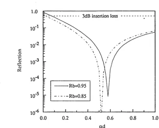
An altern ativ e a p p ro ach to the AFPM , w hich uses a b so rp tio n m odulation, is to consider phase m odulation in a MQW, this m ay also be useful in beam steering applications. The conventional approach is to operate well aw ay from the band-gap, on the long w avelength side, so as to reduce absorption. Then the change in refractive index, linked to the change in absorption by the Kramers-Kroenig relationship, changes the path length and thus the phase of the optical beam. However, because one operates at a region of low absorption the changes in refractive index tend to be weak, this usually requires the use of w aveguide geom etries in o rd er to obtain ad eq u ate m odulation. A novel approach is to use the vertical geom etry of an AFPM [Pezeshki et al]. The equation governing the total reflectivity of the AFPM at resonance is given
where R^. = effective back reflectivity - 2 a /
The absorption is varied until Ry goes through a m inim um equal to zero, at which point the front reflectivity equals the effective back reflectivity. O n one side of the m atching condition the loss due to absorption is too low to balance the equation, on the other too large. How ever, the reflected beam s to the left and right of the m atching condition differ in phase by 180°. This is because Rf and Rb are o u t of phase, and Rf dom inates w hen the absorption is high and Rb dom inates w hen the absorption is low. At a particular applied bias, and thus change in absorption, it is possible to change phase w hilst m aintaining a reflectivity of constant optical intensity. Large phase changes w ith low values of applied bias are thus possible. The disadvantage of this approach, using absorption changes to produce a phase change, is the insertion loss, although this will be com parable to AFPM absorption m odulators. It is im p o rtan t to note th at in a conventional AFPM there will also be som e phase change, although as one is not crossing the m atching point it will be greatly reduced. It has been estim ated by [Pezeshki et al] to be =20°. This w ould still result in less chirp than w aveguide devices.
We previously discussed how wavelength m ultiplexing could vastly increase the quantity of inform ation transm itted. A step tow ards such a system is an integrated w avelength dem ultiplexer receiver, which has been dem onstrated in G aln A sP /In P [Bornholdt et al]. This used two w avelengths ro u ted by an integrated sym m etric directional coupler. It m ay well be that the MQW could also be used as a w avelength dem ultiplexer since its responsivity is governed by the b ias-d ep en d en t absorption spectra. One could then operate it as a voltage tuneable, w avelength dependent photodetector.
1.3.7 Integrated Waveguide Structures
enorm ous am ount of w ork still to be done in either area. In the future these technologies are likely to prove com plem entary, so it is w orthw hile looking briefly at w aveguide integrated optics and how they m ay relate to future optoelectronic systems.
The w aveguide u sed m ay typically be a b u ried h eterostructure in w hich the light is tightly confined by tw o sem iconductors of different refractive index, and the dim ensions m ay be =0.2x1 pm wide. The loss per cm is only a few percent per centim etre of p ro p ag atio n distance, and w ould therefore not be a problem w ithin an integrated circuit. The w aveguide can also be absorbing, in which case it is term ed active, and m ay then be used to form a m odulator or laser w ithin the plane of the chip. The use of corrugated w av eg u id e g ratin g s (or D istrib u ted Bragg Reflectors) as laser cavity reso n ato rs elim inates the need for cleaved facets, an d has led to the distributed feedback laser. The sam e type of gratings m ay also be used as filters in m ultiple-w avelength systems. By injecting a current across the DBR one can create a change AN which will change the reflectivity band.
An exam ple of w hat can be achieved is the M ultisection MQW-DBR laser [Koch and Koren] This has an o u tp u t of 20-30mW, a m inim um AX of 1- 2MHz, and allows IG H z tuning (80Â) at 1.53pm. Such a device offers the p o ten tial for m u ltich an n el, coherent n e tw o rk s w ith q u a n tu m lim ited detection sensitivity. These channels could be detected, filtered and then routed to the processing optoelectronics, all by w aveguide technology.
13.8 Self Electrooptic Effect Devices
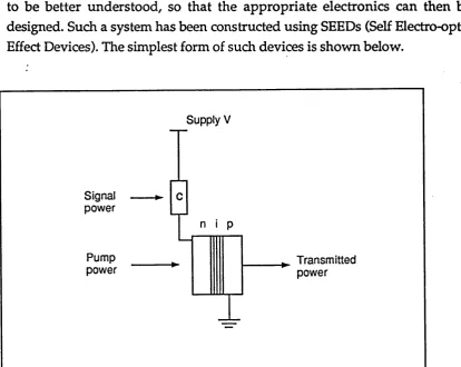
To take a step nearer the system in Fig 1.4, consisting of tw o dim ensional electronic arrays w ith free space interconnecting optics, it w o u ld be useful to first research the properties of tw o dim ensional arrays. O n e approach is to build a 2-d array having optical inputs an d o u tp u ts only, i.e. to dispense w ith the electronic processing stages. This brings th e fabrication to w ith in the limits of presen t day technology, and also allow s the properties of 2-d arrays to be b etter u n d ersto o d , so th at the a p p ro p ria te electronics can then be designed. Such a system has been constructed using SEEDs (Self Electro-optic Effect Devices). The sim plest form of such devices is show n below.
Supply V
Signal power
Pump power
n I p
Transmitted power
Figure 1.5 Diagram showing the operation of a basic self electro-optic effect device (SEED).
In the figure above C m ay be a photodiode, a phototranistor, another MQW m odulator, a FET, or even sim ply a resistor. In the latter case there is no separate signal pow er beam, there being a single in p u t beam incident on the
causing a voltage drop across the resistor, hence reducing the voltage across the diode. This leads to an increase in the absorption of the MQW diode, increased photocurrent, and so on, in a positive feedback loop u n til the voltage across the diode can get no smaller. We thus have sw itching into a high absorption (low transm ission) state. The reverse process also occurs leading to a bistable device, having either low or high transmission. Choosing a photodiode instead of a resistor gives an extra degree of control via the second optical input beam, and results in im proved perform ance [Miller 90].
A m ore sophisticated form of the device is the S-SEED, or sym m etric- SEED, which consists of two MQW pin diodes connected in series, so th at each node has two optical inputs and two optical outputs. W hen one diode is 'on' the other is forced 'off, i.e. one is absorbing and the other is transm itting. The device is bistable, and its state is changed by the ratio of the tw o in p u t beams, and not by the absolute beam intensity. This is likely to result in m ore reliable operation as attenuation of the beam is less critical.
A lthough having bo th optical in p u ts and o u tp u ts these are still optoelectronic devices. SEEDs have been operated at 35pS sw itching tim es, and the limit is, perhaps, IpS or less. They are far too energy consum ptive at present for large system s, b u t they are ideal for exploring 2-d arrays, and have been used to dem onstrate sw itching system s [1.106]. These could point the way forw ard in which a complete optoelectronic island array could be developed. For instance, by integrating a transistor to provide gain w ith the SEED device, the optical pow er required is reduced, an d the benefits of electronics and optics dem onstrated. In the fu tu re w e can expect to see intense research into the exact types of architecture w hich w ould be m ost beneficial, and the optical devices that w ould be m ost appropriate. It seem s likely, how ever, that an efficient optical m odulator w ould play a key p art in such a system and that integration on silicon w ould be a desirable option.
13.9 Optoelectronics in Switching Systems
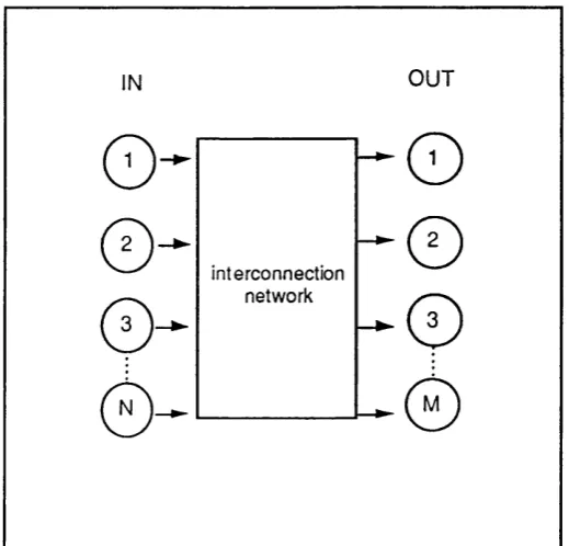
telecom m unications b u t also in a p arallel co m p u ter to lin k processors, m em ories, and I /O controllers. M ultistage netw orks have been found to be b est a t red u c in g bottlenecks an d p ro h ib itiv e co m p lex ity (th e o th er architectures th at may be used are bus and crossbar). Some system s employ self-routing, by which the packets of data, each having an address header, can find their w ay through the netw ork. These have the potential for both high th ro u g h p u t an d rap id refiguring, b u t im ply the use of d istrib u te d logic throughout the switching system. Each node of the netw ork reads the address a n d sets its sw itch accordingly, eith er p assin g it stra ig h t th ro u g h or "exchanging" it. Of course this m ust be done before the arrival of the data itself, or if not, at least a facility for buffering the data m ust be provided. The sim plest 2x2 switch is illustrated in Fig 1.7. A row of such elem ents m ay form a stage, and a num ber of stages forms a netw ork. The digital logic to perform the decoding and switching m ust therefore be very fast and efficient, which su g g ests the u se of electronics. H ow ever, a n u m b er of p ro b lem s are encountered in these systems: clockskew, lim ited p in -in /p in -o u t, physically large system s, and electrical signal crosstalk. The ideal transm ission m edium for such large quantities of data is optics, so once again the preferred solution m ay be an optoelectronic one consisting of electronic islands controlling the optical sw itching of data.
IN O U T
0
-
- o
interconnection
©
-network
-Figure 1.7 2x2 switching element
Various technologies have been proposed for the sw itching of optical data streams. For example, four port directional couplers have been dem onstrated in Lithium N iobate, in w hich pow er crosses over d ep en d in g on the phase relationship of the two w aveguides, which is in tu rn controlled by voltage applied to tw o electrodes. These devices typically have large capacitance and req u ire 5 to 20V to sw itch, the drive req u irem en ts therefore p resen t a problem . M oreover, they also p resen tly suffer from larg e atten u atio n , crosstalk, and are slow to reset, requiring 3 to 6 nS. Increasing the num ber of ports results in exceedingly complex devices to fabricate, the present state of the art being a 128x128 device bu ilt from 4x4 blocks [Burke et al]. Because such devices retain the data signal in the optical dom ain they have enorm ous potential th ro u g h p u t of data, b u t the reconfiguration tim es are slow. They w ould therefore seem m ore suited to routing large blocks of traffic, rather than sorting small packets of data.
A n altern ativ e technology is that u sin g MQW m o d u lato rs, w hich retains all the advantages of scale and integration provided b y conventional sem iconductor technology. The level of electronic intregration could range from a sim ple resistor if R-SEEDS were em ployed, in w hich the switching is a function of the incident optical pow er, to an electronic logic circuit decoding the ad d ress an d hence controlling an AFPM m odulator. Either approach w ould be ideal for 2-d arrays of sources and receivers, u sing m icrolenses a n d /o r holographic lenses for the free space imaging.
optoelectronic system w as designed along the lines described above, and assum ed a high degree of integration betw een the MQW devices and the silicon electronics islands i.e. a G aA s/S i approach w ith transm itting and receiving m odulators, and free space im aging optics. The key perform ance issues in such system s are the speed, the system th ro u g h p u t (the speed times the netw ork size), the pow er consum ption, and the floorprint area. The m ost appropriate, b u t functionally equivalent, topologies for the two technologies are the 2-d shuffle for optoelectronics, a n d the B anyan for electrical interconnects, which m inim izes the num ber of w ire crossovers, and is m ore efficient in terms of pow er consum ption and footprint area.
An 8x8 Banyan sw itching netw ork is show n in Fig 1.8. It is built from
2x2 sw itching elements, in three stages, each of which w orks on subsequent bits of the destination address. The data is routed to the u p p er o u tp u t if the sw itching elem ent sees a 0, and the lower o u tp u t if it sees a 1. By following the p ath s th ro u g h it can be seen th at the d ata will fin d its destination regardless of the in p u t it uses. A num ber of assum ptions w ere m ade for the CMOS VLSI implementation.:- the elements w ould be arranged in rows; tw o layers of interconnect w ould be used, one for horizontal paths, the other for vertical paths; and all the elem ents w ould be integrated on one chip. In current systems m any chips are often interconnected by transm ission lines. These m ay have faster propagation rates, b u t have problem s of ground loops, crosstalk, reflections, and high pow er consum ption. The process assum ed was 1.2pm 5V CMOS w ith a m inim um feature size of 0.6pm, the w ire pitch w as taken as 2.4pm w ith a capacitance of 2 p F /c m an d a resistance of 375W /cm. The pow er consum ption of the netw ork envisaged is a function of the num ber of gates operating, the clock speed, and the energy charging and discharging the wires.
— 0000
The optoelectronic im plem entation assum ed 5pm x 5pm MQW m odulators integrated w ith Si CMOS electronics, operating at a w avelength of 850nm and w ith a 5V drive voltage. The m odulator m ay ap p ear optim istically sm all, given som e of the problem s of alignm ent we discussed earlier, b u t on the other hand the detector size was taken as a m ore generous 20pm x 20pm. The pow er consum ption of the optoelectronic netw ork w ould be a function of the electronic switches; the m odulators and their drivers; and the detectors an d their amplifiers.
Obviously in an exercise like this, w here so m any assum ptions have to be m ade, it w ould be unw ise to expect to derive definitive quantitative results as to the m erits of both approaches. However, the general trends are certainly w orthy of note. In term s of clock speed the VLSI im plem entation could be operated at high speed (lOOMHz) for small netw orks (N<256), b u t as the size increased the operating speed was found to be constrained because of delay in the longest wires, whilst the optoelectronic netw ork speed w as found to be in d ep en d en t of the netw ork size. In term s of th ro u g h p u t the VLSI system reached a saturation point, for as the netw ork size increased the clock speed h ad to be reduced. This restriction did not ap p ly to the optoelectronic netw ork so the throughput kept on increasing as the netw ork w as expanded. Pow er co n su m p tio n for sm all netw orks w as fo u n d to be sim ilar, b u t com parison for larger netw orks was difficult. This w as because the clock speed had to be reduced for the VLSI network, naturally resulting in reduced pow er consum ption com pared to the optoelectronic netw ork. If, how ever, the VLSI netw ork could be m aintained at its original clock speed, its p o w er consum ption w ould be higher. This is a direct result of the factors discussed in the energy comparison betw een optical and electronic interconnects. As the netw ork size is increased the scalability favours the optoelectronic netw ork, because of its use of parallel inputs and o u tp u ts, w hile w irin g of th e electronic netw ork becomes increasingly complex. This also m eans th at the optoelectronic system will have a smaller footprint for large networks.
2.1 INTRODUCTION TO QUANTUM WELLS
To u n d erstan d the effect of strain on the absorption spectra of the MQW structures, it is first necessary to in troduce the basic theory th at governs absorption in unstrained q u antum wells. W e start by ignoring the excitons them selves, w hich result from electron-hole coulom b interaction, an d only consider the effect of confinem ent on free electrons and holes. These are norm ally described by the effective mass approxim ation, in w hich an effective m ass is given to each particle according to its diffraction th ro u g h the sem iconductor lattice, due to the periodic potential of the u n it cells. External potentials are ignored and the resulting band structure for bulk crystal can be used in the solution to the quantum well. The EMA has been found to be very successful in p red ictin g the resu ltin g ab so rp tio n characteristics despite changes in the external potential occurring on an atom ic scale in quantum well structures. The confinement due to the m ultilayer structure has the effect of firstly quantizing the m otion of the electrons and holes perpendicular to the layers, and secondly introducing a different sym m etry to that of the bulk material. This in turn results in new selection rules for optical transitions, and changes the hole masses, particularly for m otion parallel to the layers.
In a real quantum well structure, for exam ple G aA s/G aA lA s, there is a finite energy gap betw een the tw o m aterials th at is sh ared betw een the conduction and valence bands such
that:-A E g = that:-A E c + that:-A E y Eqn 2.1
w e shall prim arily concern ourselves w ith the form er case of non-interacting wells. The physics of which can be described by considering a single quantum well, an d are not dependent on the num ber of wells present, these only serve to enhance the m agnitude of the absorption or phase changes observed.
The real quantum well structures w ith finite barriers are rather difficult to analyse theoretically so it is instructive to first consider the exam ple of a single, infinitely deep w ell for w hich a parabolic, n o n -d eg en erate b and stru ctu re is assum ed in the bu lk m aterial. For this m odel the im p o rtan t features resulting from q u antum confinement can be deduced, an d an exact solution to Schroedinger's equation calculated.
In the plane of the layers there is no confinem ent and so the electrons and holes can m ove freely w ith the usual dispersion
laws:-E (k) = laws:-E 2+ lc ■
c ' •' g 2m I X y e
Eqn 2.2a
Eqn 2.2b
Perpendicular to the layers the electrons and holes are confined, and since we have assum ed an infinite well the am plitude of the envelope w ave functions m ust be zero at the barrier walls. Therefore the w avefunctions become
:-Sin Eqn 2.3
w here Lz = the layer thickness, and (j-1) =0,1,2.. are the num ber of nodes of the wavefunctions. The Eigenenergies will be
:-E; =
---' 2me , h
Eqn 2.4
Figure 2 . 1 Energy levels in an infinite quantum well
The optical absorption will be governed by the above transition energies and the joint density of states. For the infinite well approxim ation this is given by
[Chemla and Miller]
g.o(E) = ^ e ( E - E , - - E , - ) Eqn 2.5
w here |i is the electron-hole reduced mass p-i = m^-i + m^"^ .
Therefore for an infinite well the absorption spectrum is a series of steps starting at AE = E^™ -Ejh°®, w ith the selection rule Aj = je - jh = 0.