University College London
O
p t ic a l c o n t r o l t e c h n i q u e s f o r m ic r o w a v ePHASE LOCKING APPLICATIONS
Ian David Blanchflower
1992
A thesis to the University of London for
ProQuest Number: 10106745
All rights reserved
INFORMATION TO ALL USERS
The quality of this reproduction is dependent upon the quality of the copy submitted. In the unlikely event that the author did not send a complete manuscript and there are missing pages, these will be noted. Also, if material had to be removed,
a note will indicate the deletion.
uest.
ProQuest 10106745
Published by ProQuest LLC(2016). Copyright of the Dissertation is held by the Author. All rights reserved.
This work is protected against unauthorized copying under Title 17, United States Code. Microform Edition © ProQuest LLC.
ProQuest LLC
789 East Eisenhower Parkway P.O. Box 1346
This thesis considers the use of optical control techniques for phase locking of microwave and millimetre wave oscillators. Optical control functions provide a convenient means of controlling high frequency circuits. With the increasing importance of optical techniques in signal distribution applications, there is further advantage to be gained from the use of optically controlled devices as optical-to- electrical transducers.
The optical phase locking systems considered are optical injection locking and optical frequency tuning within a phase locked loop. A third system, applying a combination of optical injection locking and optical frequency tuning within a phase locked loop, is considered in detail for the first time. General analytical models for the systems are derived and used to compare the operation. The analysis is effective in deriving new results for the effects of loop delay and differential phase in the novel optical injection locking/phase locked loop combination. Practical systems are demonstrated, employing an optically controlled 1.5 GHz MESFET oscillator. The results of optical frequency tuning and optical injection locking effects are presented, including a frequency tuning modulation response up to 100 MHz, and optical injection locking ranges up to 2 MHz. Measurements performed on the optical phase locking systems confirm the validity of the analysis.
The practical implementation of optical phase locking systems is discussed. The analysis shows that phase locked loop bandwidths in excess of 100 MHz are feasible with a moderate optical tuning sensitivity of 10 MHz/mW. The performance of practical systems, however, may suffer from limited tuning modulation bandwidths, frequency tuning range, and poor tuning linearity that are characteristic of some optically tuned oscillators. Optical injection locking is dependent on the operating conditions of the oscillator, and this restricts its application, and that of the combined injection locking/PLL system. Fractional locking bandwidths of up to 1% with a few mW of optical signal power are possible with present devices. Improvements in device design for optical access may allow bandwidths of several hundred MHz in millimetre wave oscillators.
Ac k n o w l e d g e m e n t
I would like to acknowledge the SERC for funding the work presented in the thesis and also Marconi Defence Systems Ltd., Stanmore for providing financial and industrial support.
To my wife, Damienne,
for her patience and understanding!
Ta b l eo f c o n t e n t s
List of illustrations List of tables Table of symbols References
Chapter 1: Introduction and overview
1.1 Introduction
1.2 Optical phase locking schemes
1.2.1 Phase lock loop schemes and injection locking 1.2.2 Optical phase and frequency control
1.3 Phase locked oscillator optical receivers 1.4 Contents
Chapter 2: Optical control of microwave and millimetre wave oscillators
2.1 Introduction
2.2 Direct optical control
2.2.1 Photoeffects and wavelength dependency 2.2.2 Gunn diode oscillators
2.2.2.1 Frequency tuning and amplitude switching 2 2 2 2 Trap effects
2.2.3 IMPATT diode oscillators 2.2.3.1 Theoretical estimate
2.2.3.2 Experimental frequency tuning 2.2.3.3 PM frequency response
2.2.3.4 Amplitude switching 2.2.3.5 Optical injection locking 2.2.4 MESFET oscillators
2.2.5.1 Frequency tuning
2.2.5.2 Optical injection locking 2.2.6 HBT oscillators
2.2.6.1 Frequency tuning 2.2.6.2 Optical injection locking 2.3 Indirect optical control
2.3.1 PIN diodes as optically controlled capacitors
2.3.1.1 Frequency tuning of a 25GHz HEMT oscillator 2.3.1.2 Frequency tuning of a 1.8 GHz DRO oscillator 2.3.2 Optically induced changes in conductivity
2.3.2.1 Optical frequency tuning 2.3.2.2 Amplitude switching 2.4 Sununary
Chapter 3: Oscillator phase locking by phase locked loop, injection locking and
injection phase locked loop
3.1 Introduction
3.2 Unified PLL models for system comparisons 3.2.1 Phase locked loops (PLL)
3.2.1.1 Non-linear dynamic equation 3.2.1.2 Small signal analysis
3.2.1.3 PLL terminology 3.2.2 Injection locked oscillators
3.2.2.1 PLL model for injection locking 3.2.3 Injection phase locked loops
3.2.3.1 Small signal analysis
3.2.4 System comparisons using unified PLL model 3.3 Operation in practical systems
3.3.1 Control loop stability
3.3.2.1 Stability in first order PLLs 3.3.1.2 Stability in second order PLLs 3.3.1.3 Stability in first order IPLLs 3.3.2.4 Stability in second order IPLLs
3.3.3 Differential delay
3.3.3.1 Differential delay effects on IPLL operation 3.3.4 Limits of PLL model for injection locking
3.3.5 Noise considerations 3.4 Summary and conclusion
Chapter 4: Characterisation of optical control effects in a MESFET oscillator
4.1 Introduction
4.2 Photocontrol mechanisms 4.2.1 Photoconductive effects 4.2.2 Photovoltaic effects
4.2.2.1 Photovoltaic gate biasing
4.2.2.2 Schottky junction layer charge redistribution
4.2.2.3 Photovoltage generation at the substrate/channel interface and back-gating
4.2.3 Other photoeffects 4.3 Experimental set-up
4.3.1 Oscillator design
4.3.2 Experimental arrangement 4.4 Photoeffects in the MESFET device
4.4.1 Gate photocurrent
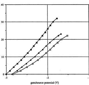
4.4.2 Optical control of channel current 4.4.2.1 Forward bias characteristics
4.4.2.2 Comparison of Vgs and optical control 4.4.3 Discussion
4.5 Optical frequency tuning
4.5.1 Direct optical frequency tuning 4.5.1.1 Results
4.5.1.2 Discussion 4.5.2 Photovoltaic bias tuning
4.5.2.1 Vgs tuning
4.5.2.2 Photovoltaic tuning
4.5.2.3 Frequency response manipulation
4.6.1 Experimental procedure 4.6.2 Results
4.6.3 Discussion 4.7 Summary
Chapter 5: Experimental investigation of optical phase locking systems
5.1 Introduction
5.2 Experimental arrangement 5.2.1 Setup details
5.2.2 Loop design 5.3 Tracking performance
5.3.1 Static phase error from frequency detuning 5.3.2 Phase error transient response
5.3.2.1 Transient response of optical injection locking 5.3.2.2 Transient response of OPLL and OIPLL systems 5.4 Oscillator phase noise suppression
5.4.1 Measurement details 5.4.2 Results
5.4.3 Discussion
5.5 Stability and effects of delay within the PLL 5.5.1 PLL instability
5.5.2 OIPLL instability 5.6 Differential delay
5.6.1 Gain competition
5.6.2 Differential delay in second order type II OIPLLs 5.7 Summary
Chapter 6: Practical optical phase locking systems
6.1 Introduction
6.2 Optical frequency tuning in a phase locked loop 6.2.1 Effective oscillator tuning constant 6.2.2 Loop amplification and loop bandwidth
6.2.3 Practical system aspects
6.2.3.1 FM frequency response 6.2.3.2 Linearity
6.2.3.3 Tuning range 6.2.4 Summary and discussion 6.3 Optical injection locking
6.3.1 Optical injection locking sensitivity
6.3.2 Optical injection locking range variation with operating conditions 6.3.3 Summary and discussion
6.4 Optical injection phase locked loop 6.4.1 Loop gain
6.4.2 Practical system aspects
6.4.2.1 OIPLL natural frequency 6.4.2.2 Pull-in operation
6.4.2.3 Differential delay
6.4.2.4 AM and PM noise effects 6.4.3 Summary and discussion
6.5 Discussion
Chapter 7: Application of phase locked receivers to optical microwave signal distribution networks
7.1 Introduction
7.2 System calculations
7.2.1 Optical transmitter
7.2.2 Optical fibre network losses 7.2.3 Sensitivity
7.2.3.1 Sensitivity in direct detection receivers 7.2.3.2 Sensitivity in OPLL
7.2.3.5 Sensitivity in OIPLL 7.2.4 lin k budget
7.3 Practical aspects of direct detection receivers 7.3.1 Gain requirements in amplification chain 7.3.2 Phase accuracy in amplification chain 7.3.3 Monolithic technology
7.4 Practical aspects of optically phase locked oscillator receivers 7.4.1 Systems
7.4.2 OPLL phase locked receivers 7.4.3 OIPLL phase locked receivers
7.4.4.1 Remote data mixing schemes 7.4.4.2 Phase priming
7.5 Summary
Chapter 8: Summaiy
8.1 Introduction
8.2 Optical phase locking systems
8.2 Use of optical control in phase locking systems 8.3 Phased array applications
Appendices
Appendix A Phase locked loop operation A/1 PLL definitions
A/2 Linear tracking A/3 Non linear tracking
A/3.1 Tracking limits: hold-in range A/3.2 Acquisition
A/4 Noise effects A/4.1 Phase noise
A/4.2 Amplitude modulation noise
Appendix B. Experimental system design
arrangement B/3 Loop design
B/3.1 Open loop gain B/3.2 Time constants
Appendix C Noise analysis of experimental OPLL C/1 Sources of noise
Appendix D. Signal-to-noise ratio in microwave direct detection PIN-FET receivers
D/1 Signal-to-noise expression D /2 Noise
D/3 Calculation
Lis t o f il l u s t r a t io n s
Fig. 1.1 Optical control of microwave oscillators
Fig. 1.2 Oscillator phase locking by phase locked loop employing optical frequency control
Fig. 1.3 Optical injection locking with closed loop control of static phase error
Fig. 1.4 Alternative methods of microwave modulated optical signal reception
Fig. 3.1 Schematic of oscillator phase locking systems
Fig. 3.2 Block diagram of phase locked loop
Fig. 3.3 Block diagram of injection locking and its equivalent phase locked loop representation
Fig. 3.4 Block diagram of injection phase locked loop assuming equivalent PLL representation of injection locking
Fig. 3.5 Simplified block diagram of injection phase locked loop used for small signal analysis
Fig. 3.6 Nyquist diagrams indicating stability in first order phase locked loops
Fig. 3.7 Nyquist diagrams for an ideal second order loop with varying the loop damping coefficient, ç
Fig. 3.8 Nyquist diagrams comparing the condition for stability in first and second order phase locked loops
Fig. 3.9 Nyquist diagrams for first order injection phase locked loops
Fig. 3.10 Nyquist diagrams for second order injection phase locked loops
Fig. 3.11 Nyquist diagram indicating the limit to the natural frequency in a second order injection phase locked loop
Fig. 3.12 Schematic of injection phase locked loop indicating the high frequency paths and their delay times
Fig. 3.13 Rationalisation of injection phase locked loop with differential delay
Fig. 3.14 Nyquist diagram showing the failure of the injection phase locked loop to meet the stability criterion when the differential phase is equal to n
Fig. 3.15 Injection phase locked loop showing the introduction of AM noise at the input to the phase locked loop component
Fig. 4.1 Cross-section view of a GaAs MESFET indicating the principal photoeffects
a load line construction for assessing the photovoltaic gate bias effect
Fig. 4.3 Detail of NEC 900000 MESFET
Fig. 4.4 MESFET small signal equivalent circuit and oscillator circuit diagram
Fig. 4.5 Experimental arrangement for the illumination experiments
Fig. 4.6 Laser power/bias current characteristics
Fig. 4.7 Gate circuit photocurrent variation with illumination power
Fig. 4.8 Ids/Vds characteristics with and without illumintion
Fig. 4.9(a) Drain-source current variation with gate-source potential
Fig. 4.9(b) Drain-source current variation with illumination power
Fig. 4.10 Frequency shift with illumination power
Fig. 4.11 Optical tuning responsivity variation with intensity modulation frequency
Fig. 4.12 Frequency tuning effect of gate-source bias potential
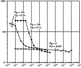
Fig. 4.13 Optically induced frequency shift due to photovoltaic gate bias (Rg = 10 kohms)
Fig. 4.14 Frequency response of overall tuning responsivity arising from photovoltaic gate bias and residual tuning effects
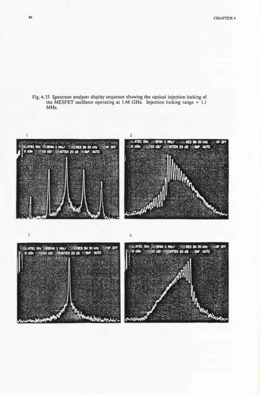
Fig. 4.15 Spectrum analyser display sequence showing the optical injection locking of the MESFET oscillator operating at 1.48 GHz. Injection locking range = 1.1 MHz
Fig. 4.16 Optical injection locking range variation with peak optical signal power
Fig. 5.1 Experimental arrangement for the OIPLL system
Fig. 5.2 Schematic of a phase locked loop using optical frequency tuning
Fig. 5.3 Static phase error variation with input signal frequency for the optically injection locked oscillator.
Fig. 5.4 Static phase error variation with input signal frequency for (a) the optically injection locked oscillator, and (b) a second order optical injection phase locked loop
Fig. 5.5 Phase transient for the optically injection locked oscillator due to switched input frequency
Fig. 5.6 Injection locking acquisition phase transient
Fig. 5.7 Phase transients for the optical phase locked loop and the optical injection phase locked loops due to switched input frequency
Fig. 5.8 Phase noise suppression by phase locking systems
Fig. 5.9 Phase noise-to-carrier ratio for phase-locked oscillator output spectrum
Fig. 5.10 Experimental arrangement for the investigation of the effects of loop delay
Fig. 5.11 Phase noise peaking in optical phase locked loop output spectrum due to loop delay
Fig. 5.12 Phase transient with switched input signal frequency for the optical phase locked loop with loop delay causing marginal stability
Fig. 5.13 Phase noise peaking in the optical injection phase locked loop output spectrum due to delay in the phase locked loop component
Fig. 5.14 Phase transients with switched input signal frequency for the optical injection phase locked loop with PLL loop delay and varying loop natural frequency
Fig. 5.15 OIPLL lock-in range variation with differential path length
Fig. 5.16 Spectrum analyser display sequence showing the failure of the optical injection phase locked loop to lock when the injection locking and phase locked loop act in opposition
Fig. 6.1 Diagram showing the practical implementation of an OPLL
Fig. 6.2 Diagram showing the practical implementation of a heterodyne OPLL
Fig. 6.3 Optical injection locking ranges in practical microwave oscillators
Fig. 6.4 Optical injection locking ranges in practical oscillators calculated assuming an optical coupling efficiency of 50%
Fig. 6.5 Diagrams showing the practical implementation of an OIPLL
Fig. 7.1 1:M optical fibre distribution network using optically phase locked oscillators
Fig. 7.2 Maximum operating powers demonstrated in semiconductor amplifiers and oscillators
Fig. 7.3 Remote data mixing scheme for the transmission of RF signals by optical fibre
modulation noise at the input of a PLL
Fig. B1 Circuit diagram for activa loop filter and laser driver
Fig. C l Schematic of experimental PLL system indicating sources of noise within the system
Fig. C2 Equivalent PLL schematic used for noise analysis
Fig. D1 SNR for a microwave optical link as a function of mean optical signal power
Lis t OF TABLES
Table 2.1 Optical absorption coefficients and absorption edges in various semiconductors
Table 2.2 Summary of optical frequency tuning techniques
Table 2.3 Summary of optically controlled microwave switching techniques
Table 2.4 Summary of optical injection locking techniques
Table 3.1 Phase locking system operating parameters
Table 4.1 Comparison of calculated and measured optical tuning responsivity at various means powers
Table 5.1 Experimental system parameters
Table 5.2 OPLL system parameters for loop delay stability measurements
Table 5.3 OIPLL system parameters for loop delay stability measurements
Table 5.4 Theoretical and measured limits to natural frequency in delay limited OIPLL
Table 7.1 Fixed and variable fibre network losses
Table 7.2 lin k budget for optical distribution network with various optical/millimetre wave receivers
Table A1 Expression for the natural frequency and damping coefficient in second order loops
Table A2 Static phase error in phase locked loops under varying input signal conditions
Table B1 Practical system loop gain parameters
Table B2 Experimentally determined time constants and loop parameters
Table D1 Values used for estimate of link SNR in Fig. D1
Symbol Unit Description
k J/K Hofmann’s constant (= 1.39 x 10^^ x ^ ) h J s P l a ^ constant (= 6.026 x 10"^* J s) q C electronic charge (= 1.6 x 10"^® C)
T K temperature
W . W microwave oscillator output power W injected microwave power
Q oscillator external loaded quality factor *o(‘) rad phase of the oscillator
«i(0 rad phase of the injected signal
"o rad s’ ^ ang. freq. of oscillator "l rad s'^ ang. freq. of locking signal
“£ rad s~^ ang. freq. of free running oscillator
Aw rad s*^
F(s) tranfer function of loop filter K , V rad”^ phase detector constant K rad s~^ V”^ oscillator tuning constant
A amplification within loop
K s - ' (= AK^Kj) overall amplification within loop H(s) — closed loop transfer function
G(s) — open loop transfer function
“n rad s'^ natural frequency of loop
damping coefficient of loop AWl rad s’ ^ lock-in range
AWg rad s"^ hold-in range AWp rad s'^ pull-in range
' " i n j rad s'^ injection locking range
K . s-^ effective amplification within inj. lock, equiv. loop G i n j W — open loop transfer function of inj. lock, equiv. loop
GpllW — open loop transfer function of PLL component of
IPLL
^BW s time constant for bandwidth limiting component in PLL
s total propogation delay within PLL
R(s) additional filtering response within loop (other than F(s))
rad phase error at oscillator
*pdW rad phase error at phase detector
^diff rad static differential phase error rad phase noise spectral density
P o l W incident optical power
P os W optical power at optical source
cm^/V s electron mobility cm ^/V s hole mobility
Jo A m”^ junction reverse saturation current density Jph A m~^ photocurrent density
♦p V hole quasi Fermi energy level
(continued)
Symbol Unit Description
Pn
m -' hole minority carrier density^Pn
m~^ change in hole minority carrier density with illuminationV V junction photovoltage arising from illumination m
W ' l / 2
modulation index of optical signal 7 optical injection locking coefficient
«„(s) rad s '^ W ^ optical tuning sensitivity of optically tuned oscillator
a optical attenuation
K.
WA"^ laser responsivityRl Ohms load resistance
F amplifier noise figure
B Hz bandwidth
n coupling effidency at photodiode of photoreceiver
V Hz frequency of photon
N V^Hz'^ noise voltage spectral density
♦n(0
W H z'^ PLL input AM noise power spectrum‘„’(0
rad^ Hz‘ ^ PLL input equivalent phase noise power spectrum Nop W H z'^ single sideband phase noise power spectral densityC W carrier power
SNR^ input signal to noise ratio RIN dBH z'^ relative intensity noise
MTR mixer noise temperature ratio
rad^ phase jitter variance
rad^ Hz"^ mean square phase jitter spectral density
Re f e r e n c e s
[1] FORREST, J.R., RICHARDS, P.P., DE SALLES, A.A., and VARNISH, P., "Optical fibre networks for signal distribution and control in phased array elements", Proc. Int. Conf. RADAR 82, London, 1982, pp. 408-412
[2] WALLINGTON, J R., and GRIFFIN, J.M, "Optical techniques for signal distribution in phased arrays", GEC Journal of Research, 1984, vol. 2, pp.66-75
[3] HERCZFELD, P R., and DARYOUSH, A.S., "Fiber-optic feed networks for large aperture phased array antennas". Microwave Journal, 1987, vol. 30, no. 8, pp. 160-166
[4] SEEDS, A.J., MCMILLAN, W.I., PESCOD, C.R., WALE, M.J., and BIRKMAYER, W.S., "Optical control of phased array antennas: a European perspective", IEEE International Symposioum on Microwave Theory and Techniques, Symposium Digest, 1990, pp. 1343-1346
[5] PANSINI, E., TESTA, F., and NORBIATO, R., "Experimental evaluation of optical signal distribution for phased array antenna". Electron. Lett., 1991, vol.27, pp. 404-406
[6] SHEEHAN, P.G., and FORREST, J R., "The use of optical techniques for beamforming in phased arrays", Proc. SPIE, 1984, vol. 477, pp. 82-89
[7] CARDONE, L., "Ultra-wideband microwave beamforming technique". Microwave Journal, 1985, vol. 29, no. 4, pp. 121-131.
[8] PAPPERT. S.A., "Ultra-widband direction finding using a fiber optic beamforming processor", Proc. SPIE, 1988, vol. 886, pp. 239-246
[9] KOEPF, G.A., "Optical processor for phased-array antenna beam formation", Proc. SPIE, vol. 447,1984, pp. 75-81
[10] TAMBURRINI, M., PARENT, R.L., GOLDBERG, L., and STILLWELL, D., "Optical feed for a phased array microwave antenna", Electon. Lett., vol. 23,1987, pp. 680-681.
[11] PAOLELLA, A., and HERCZFELD, P R., "Optical control of a GaAs MMIC tranmit/receive module". International Symposium on Microwave Theory and Tech. 1988, Symposium Digest, pp. 959-962
[12] JEMISON, W.D., BERCEU, T., PAOLELLA, A., HERCZFELD, P R., and JACOMB-HOOD, A.W., "Optical control of a digital phase shifter". International Symposium on Microwave Theory and Tech. 1990, Symposium Digest, pp. 233-236
[13] LAM, D.K.W., and MACDONALD, R.I., "GaAs optoelectronic mixer operation at 4.5 GHz", IEEE Trans. Electron. Dev. 1984, vol. 31, pp. 1766- 1768
optically pumped mixer", lEE Proc. Ft. J, 1989, vol. 136, pp. 99-96
[15] NI, D.C., FETTERMAN, HR., and CHEW, W., "Millimetre-wave generation and characterisation of GaAs PET by optical mixing", IEEE Trans. Microwave Theory and Tech. 1990, vol. 38, pp. 608-614
[16] BUCK, D C., and CROSS, M.A., "Optical injection locking of PET oscillators using fibre optics", IEEE International Symposium on Microwave Theory and Techniques, 1986, Symposium Digest, pp. 611-614
[17] DARYOUSH A.S., "Optical synchronization of millimeter-wave oscillators for distributed architectures", IEEE Trans. Microwave Theory and Tech., 1990, vol. 38, pp.467-476
[18] KIEHL» R.A., "Novel optical control techniques for solid state radar transmitters", IEEE Trans. Microwave Theory and Techniques, 1980, vol. 28, pp. 409-413
[19] SEEDS, A.J., BLANCHFLOWER, ID., GOMES, NJ., KING, G., FLYNN, S.J., "New developments in optical control techniques for phased any radar", IEEE International Symposium on Microwave Theory and Techniques, 1988, Symposium Digest, pp. 905-908
[20] BLANCHFLOWER. I D., and SEEDS, A.J., "Optical phase and frequency control of a microwave oscillator". Electron. Lett., 1989, vol. 25, pp.359-360
[21] DARYOUSH, A.S., FRANCISCO, M., SAEDI, R., POLIFKO, D., and KUNATH, R., "Phase control of optically injection locking oscillators for phased arrays", IEEE Symposium, Microwave Theory and Techniques,
1990, Symposium Digest, pp. 1247-1250
[22] ADLER R., "A study of locking phenomena in oscillators", Proc IRE, 1946, vol. 34, pp.351-357
[23] ESMAN, R.D., GOLDBERG, L., and WELLER, J.F., "Optical phase control of an optically injection locked FET microwave oscillators", IEEE Trans. Microwave Theory and Techniques, 1989, vol. 37, pp.1512-1518
[24] PETER, M., and STRANDBERG, M.W.P., "Phase stabilisation of microwave oscillators", Proc. of the IRE, 1955, pp. 869-873
[25] MACKAY, R.C., "Injection locking of klystron oscillators", IRE Trans, on Microwave Theory and Techniques, 1962, pp. 228-235
[26] SATO, G., "Stabilised oscillators by using injection locking and phase- locked loops". Electronics and Communications in Japan, 1971, vol. 54, pp.59-65
[27] MURAKAMI, K., "A new phase lock demodulator with injection locking". Electronics and Coimnunications in Japan, 1969, vol. 52, pp. 119-120.
[28] SEEDS, A.J. and FORREST, J R., "Initial observation of optical injection locking of an X-band IMP ATT oscillator". Electron. Lett., 1978, vol. 14, pp. 829-830
[29] DE SALLES, A.A. and FORREST, J R., "Initial observation of optical injection locking of GaAs metal semiconductor Held effect transistor oscillators", Appl. Phys. Lett., 1981, vol. 38, pp. 392-394
[30] BANGERT, A., and LUDWIG, M., "A direct optical injection locking 8 GHz MMIC oscillator", IEEE Symposium, Microwave Theory and Techniques, 1991, Symposium Digest, pp. 499-502
[31] BANGERT, A., and LAUTERBACH, Th., "Initial observations of optical injection locking of oscillators using heterojunction bipolar transistors". Electron. Lett., 1992, vol. 28, pp. 621-623
[32] AUSTIN, J., and FORREST, J.R., "Design concepts for active phased-array modules", lEE Proceedings, Pt. F, 1980, Vol. 127, pp.290-300
[33] WARD. C.J., and FORREST, J R., "Fast acquisition phase-locked loops for frequency agile pulsed radar systems", lEE Proceedings, Pt. H, 1983, vol.
130, pp.489-494
[34] SIMONS, R., "Optical control of microwave devices", Artech House, USA, 1990.
[35] "Handbook of optical contants of solids", Ed. D. Palik, Academic Press, San Deigo, 1985.
[36] PEASALL, T.P. "GalnAsP alloy semiconductors", Wiley-Interscience, 1982.
[37] CARRUTHERS, T.F., WELLER, J.F., TAYLOR, H.F., and MILLS, T.G., "Oscillation burst generation in transferred electron devices with picosecond optical pulses", Appl. Phys. Lett., 1981, vol. 38, pp.202-204
[38] HAYDL, W.H. and SOLOMAN, R., "The effect of illumination on Gunn oscillators in epitaxial GaAs", IEEÈ Trans. Elect. Dev., 1968, vol. 15, pp. 941-942
[39] SEWELL, K.G., and BOATNER, L.A., "Multimode operation in Gunn oscillator induced by cooling and illumination", Proc. IEEE, 1967, vol. 55, pp. 1228-1229
[40] GUETIN, P., "Interaction between a light beam and a Gunn oscillator near the fundamental edge of GaAs", Journal of Appl. Phys., 1969, vol. 40, pp. 4115-4122
[41] SEEDS, A.J., SINGLETON, J. F., BRUNT, S. P., and FORREST, J. R., "The optical control of IMP ATT oscillators". Journal of Lightwave Tech., 1987, vol. LT-5, pp. 403-411
domain modeling of avalanche diodes", IEEE Trans. Electron Dev. 1979, vol. ED-26, pp. 1718-1729
[43] W A S, H.P., GUTMANN, R J., and BORREGO, J.M., "Electrton and hole photocurrent effects on IMPATT oscillators", lEE Proc. Pt. 1,1980, vol. 127, pp. 126-132
[44] SEEDS, AJ., and DE SALLES, A.A., "Optical control of microwave semiconductor devices", IEEE Trans. Microwave Theory and Techniques, 1990, vol. MTT-38, pp. 577-584
[45] SINGLETON, J.F., SEEDS, AJ., and BRUNT, S.P., "Optical control of W- band IMPATT oscillators", lEE Proceedings, Pt. J, 1986, vol. 133, pp. 349- 352
[46] CHUI, C., and FREYER, J., "Frequency modulation of IMPATT diodes by optical illumination", lEE Proceedings, Pt. 1,1984, vol 131, pp. 28-30
[47] KIEHL, R.A., "Optically induced AM and FM in IMPATT diode oscillators", IEEE Trans. Electron Dev. 1980, vol. 27, pp. 426-432
[48] YEN, H.W., BARNOSKI, M.K., HUNSPERGER, R.G., and MELVILLE, R.T., "Switching of GaAs IMPATT diode oscillators by optical illumination", Appl. Phys. Lett., 1977, vol. 31, pp. 120-122
[49] YEN, H.W., "Optical injection locking of Si IMPATT oscillators", Appl. Phys. Lett., 1980, vol. 36, pp. 680-683
[50] DE SALLES, A.A., "Optical control of GaAs MESFETs", IEEE Trans, Microwave Theory and Tech., 1986, vol. MTT-34, pp. 812-820
[51] MIZUNO, H., "Microwave characteristics of an optically controlled GaAs MESFET', IEEE Trans. Microwave Theory and Tech., 1983, vol. MTT-31, pp. 596-600
[52] SUN, H.J., GUTMANN, R.J., and BORREGO, J.M., "Photoeffects in common-source and common-drain microwave GaAs MESFET oscillators", Solid-State Electron., 1981, vol. 24, pp. 935-940
[53] SUN, H J., GUTMANN, R.J., and BORREGO, J.M., "DC and pulse-light illuminated optical responses of microwave GaAs MESFET oscillators", lEE Proceedings, Pt. 1,1984, vol. 131, pp. 31-37
[54] LORIOU, B., GUENA, J., and SAUTERAU, J.F., "Optical frequency modulated GaAs MESFET oscillator". Electron. Lett., 1981, vol. 17, pp. 901-902
[55] GOLDBERG, L., RAUSCHER, C., WELLER, J.F., and TAYLER, H.F., "Optical injection locking of X-band FET oscillator using coherent mixing of GaALAs lasers," Electron. Lett., 1983, vol. 19, pp. 848-850
[56] WARREN, D., GOLIO, J.M., and JOHNSON, E., "Simulation of optically injection-locked microwave oscillators using a novel SPICE model", IEEE Trans. Microwave Theory and Tech. 1988, vol. 36, pp. 1535-1539
[57] DE SALLES, A.A., and ROMERO, M.A., "AIq ^Gslq ^As/GaAs HEHTs
under optical illumination", IEEE Trans. Microwave Theory and Techniques, 1991, vol. M i 1-39, pp. 2010-2017
[58] SZE, S.M., Physics of semiconductor devices, 2nd edition, New York, Wiley, 1981.
[59] DODABALAPUR, A., and CHANG, T.Y., "High-gain InGaAlAs/InGaAs heterojunction bipolar tansistors and phototransistors", IEEE Electron. Dev. Lett., 1991, vol. 12, pp. 693-695
[60] SAEDI, R., BERCELI, T., DARYOUSH, A.S., and HERCZFELD. P R., "Optically controlled K-band oscillator," IEEE International Symposium, Microwave Theory and Tech., 1990, Symposium Digest pp. 293-294
[61] DARYOUSH A.S., BELAGA, M., HERCZFELD, P.R., and ROSEN, A., "Optically controlled microwave oscillators," International Conference SBMO, 1987, Digest pp. 977-982.
[62] HERCZFELD, P.R., DARYOUSH, A S., and CONTARINO, V.M., "Optically tuned and modulated microwave oscillator circuits", Proc. SPIE,
1984, vol. 517, pp. 48-56
[63] YU, Z., and LIN, W., "A new way to optically control a millimeter wave oscillator", IEEE Trans. Microwave Theory and Tech., 1990, vol. MTT-38, pp. 1360-1362
[64] ANDERSSON, I.L., and ENG, S T., "Phase and amplitude characteristics of InP:Fe modified interdigitated gap photoconductive microwave switches", IEEE Trans. Microwave Theory and Tech., 1989, vol. M IT-37, pp. 729-733
[65] WEBER, N., "New reflection-type optoelectronic microwave switch for CW applications". Electronic Lett., 1990, vol. 26, pp. 455-456
[66] UHDE, K., and EIMERTENBRINK, R., "Design and applications of optically controllable finline structures", IEEE Trans. Microwave Theory and Tech., 1990, vol. MTT-38, pp. 679-683
[67] VAN DER POL, B., "The nonlinear theory of electric oscillations", Proc. IRE., 1943, vol. 22, no. 9, pp. 1051-1086
[68] KUROKAWA, K., "Injection locking of microwave solid state oscillators", Proc. IEEE, 1973, vol. 61, pp. 1386-1410.
[69] BISWAS, B.N.,CHATTERJEE, S., SARDAR, S., BHATTACHARYA, A.K., and RAY, S.K., "Bias-tuned injection-locked discriminators", IEEE Trans. Microwave Theory and Tech. 1987, vol. 35, pp. 812-818
and reduced output phase jitter", IEEE Trans. Com., 1976, vol. 24, pp. 636- 644
[80] BERENGUER, J., BARA, J., ARTAL, E., C O R B EU A I-, and COMERON, A., "Improvements of the pull-in range and acquisition time of a microwave PLL system by injection locking the VCO", Proceedings of the Annual Frequency Symposium, 1987, pp. 524-526
[81] NYQUIST, H, "Regeneration theory". Bell Systems Tech. Journal, vol. 11, 1934; discussed in JACOBS, O.L.R., "Stability in linear systems". Chapter 3 in Introduction to control theory, Oxford University Press, London, 1974
[82] DARLING, R.B., "Transit time photoconductivity in high-field FET channels", IEEE Trans. Electron Devices, 1987, vol. 34„ pp'. 433-443
[83] CHATURVEDI, G.J., PUROHIT, R.K, and SHARMA, B.L., "Optical effect on GaAs MESFETs", Infrared Phys. 1983, vol. 23, pp. 65-68
[84] SIMONS, R.N., and BHASIN, K.B., "Analysis of optically controlled microwave/millimetre-wave device structures", IEEE Trans. Microwave Theory and Techniques, 1986, vol. 34, pp. 1349-1355
[85] GRAFFEUIL, J., ROSSEL, P., and MARTINOT, H., "Light-induced effects in GaAs FETs", Electron. Lett., 1979. vol. 15, pp.439-440
[86] NOAD, J.P., KARA, E.L., HUM, R.H., and MACDONALD, R.I., "FET photodetectors: a combined study using optical and electron-beam stimulation", IEEE Trans. Electron Devices, 1982, vol. 29, pp. 1792-1797
[87] PAPAIONONNOU, G.J., and FORREST, J R., "On the photoresponse of GaAs MESFETs: backgatin and deep trap effect", IEEE Trans. Electron Devices, 1986, vol. ED-33, pp. 373-378
[88] MISHRA S., SINGH, V.K., and PAL, B.B., "Effect of radiation and surface recombination on the characteristics of an ion-implanted GaAs MESFET’, IEEE Trans. Electron Devices, 1990, vol. 37, pp. 2-9
[89] LADBROOKE, P.H., and BLIGHT, SR., "Low-field low-ffequency dispersion of transconductance in GaAs MESFETs with implications for other rate-dependent anomalies", IEEE Trans. Electron Devices, 1988, vol. 35, pp. 257-267
[90] GOLIO, J.M., MILLER, M.G., MARACAS, G.N., and JOHNSON, D.A., "Frequency-dependent electrical characteristics of GaAs MESFETs", IEEE Trans. Electron Devices, 1990, vol. 37, pp. 1217-1226
[91] DE SALLES A.A., "An analysis of the optical injection locking of GaAs MESFET oscillators", Proc. SPIE, 1984, vol. 447, pp. 114-118
[92] WARREN, D., GOLIO, J.M., and JOHNSON, E., "Simulation of optically injection locked microwave oscillators using a novel SPICE model", IEEE Trans. Microwave Theory and Tech., vol. MTT-36,1988, pp. 1535-1539.
[93] WHITE, T.M., and JONES, W.B., "Frequency transients in sybnchronised oscillators", IEEE Trans. Circuit Theory, 1964, vol. ? pp. 279-280
[94] WAKE, D., SPOONER, T.P., PERRIN, S.D., and HENNING, I.D., "50 GHz InGaAs edge-coupled PIN photodetector", Electron. Lett., 1991, pp. 1073-1075
[95] Mitsubishi optoelectronic 1990, Optical semiconductor devices and optical- fiber communication systems, component catalogue
[96] WARD, C.J., "Delay reduction techniques in phase locked loop amplifiers", Electron. Lett. 1981, vol. 17, pp. 253-255
[97] GARBUZOV, D.Z., ANTONISHKIS, N.Y., BONDAREV, A.D., GULAKOV, A.B., ZHIGULIN, A.N., KATSAVETS, N.I., KOCHERIGIN, A.V., and RAFAILOV, E.V., "High-power 0.8/im InGaAsP-GaAs SCH SOW lasers", IEEE Journal of Quantum Elect. 1991, vol. 27, pp. 1531-1535
[98] HOWES, M.J., and MAZONAS, B.R., "Design of microwave oscillators", in Microwave Solid-State Component and Subsystem Design, Proceeding of the 1983 Leeds lEE Microwave Summer School, Ed. D.V. Morgan, MJ. Howes, and R.D. Pollard, 1983, pp. 150-182
[99] BLAUVELT, H., and LAU, K., "High signal to noise spectrum of fibre optic links to 18 GHz", IEEE Internation Symposium, Microwave Theory and Tech. 1988, Symposium Digest, pp. 979-981
[100] PAN, J.J., "21 GHz wideband fiber optic link", IEEE Intemation Symposium, Microwave Theory and Tech. 1988, Symposium Digest, pp. 977-980
[101] ESMAN, R.D., GOLDBERG, L., and WELLER, J.F., "0.83 and 1.3 micron microwave (2-18 GHz) fiber-optic links using directly modulated laser sources", IEEE Intemation Symposium, Microwave Theory and Tech. 1988, Symposium Digest, pp. 973-976
[102] STEPHENS, W.E., and JOSEPH, T.R., "System characteristics of direct modulated and externally modulated RF fiber-optic links". Journal of Lightwave Tech. 1987, vol. 5, pp. 380-387
[103] SWITZER, D.L., and JAMES, S.P., "A DC to 20 Ghz externally modulated fiber-optic link", lEE Colloquium, Optical control and generation of microwave and millimetre wave signals, 1989, London, pp. 1/1-1/5
[104] FORREST, J R., "Optical techniques for signal distribution and control in advanced radar and communication systems", AGARD Conference Proceedings No. 362, Digital Optical Circuit Technology, Germany, Sept. 1984, (Neuilly sur Seine, France, AGARD 1985), pp. 16/1-4
[105] BUI, L.Q., ALON, Y., and MORTON, T., "94 GHz, FMCW radar for low visibility aircraft landing system", IEEE Symposium, Microwave Theory and Techniques, 1991, Symposium Digest, pp. 1147-1150
Inc, London, 1984
[107] BOWERS, J.E., HEMENWAY, B.R., BRIDGES, T.J., and BURKHARDT, E.G., "26.5 GHz bandwidth InGaAsP lasers with tight optical confinement’*. Electron. Lett., 1985, vol. 21, pp. 1090-1091
[108] MELAND, E., HOLSTROM, R., SCHLAFER, J., LAUER, R.B., and POWAZINIK, W., "Extremely high-frequency (24 GHz) InGaAsP diode lasers with excellent modulation efficiency". Electron. Lett., 1990, vol 26, pp. 1827-1829
[109] CHENG, W.H., BUEHRING, K.D., APPELBAUM, A., RENNER, D., SHIN, S., SU, C.B., MAR, A., and BOWERS, J.E., "High-speed and low- relative-intensity noise 13 /^m InGaAsP semi-insulating buried crescent lasers", IEEE Journal of Quantum Electron. 1991, vol. 27, pp. 1642-1646
[110] KAWANO, K., KITOH, T., JUMINOJI, H., NOZAWA, T., and YANAGIBASHI, M., "New tranvelling-wave electrode Mach-Zehnder optical modulator with 20 GHz bandwidth and 4.7 GHz driving voltage at 1.52 Atm wavelength". Electron. Lett., 1989, vol. 25, pp. 1382-1383
[111] NAZARATHY, M., DOLFI, D.W., and JUNGERMAN, R.L., "Spread spectrum frequency response of coded reversal traveling wave modulators", IEEE Journal of Lightwave Tech. 1987, vol. 5, pp. 1433-1443
[112] WALKER, R.G., "high-speed III-V semiconductor intensity modulators", IEEE J. of Quantum Electronics, 1991, vol. 27, pp. 654-667
[113] NEES, J., WILLIAMSON, S., and MOUROU, G., "100 GHz travelling wave electro-optic phase modulator", Appl. Phys. Lett., 1989, vol. 54, pp.
1962-1964
[114] VAN ECK, T.E., WALPITA, L.M., CHANG, W.S.C., and WIEDER, H.H., Tranz-Keldysh electrorefraction and electroabsorption in bulk InP and GaAs", Appl. Phys. Lett, vol 48, pp 451-453,1986.
[115] WATIKA, K., KOTAK, I, MITOMI, O, ASAI, H., and KAWAMUTA, Y., "High speed InGaAs/InAlAs multiple quantum well optical modulators with bandwidths in excess of 40 GHz at 1.55 A*m", Proc. Conf. Lasers Electro-Opt. 1990, Tech. Dig., vol. 7, pp. 70-71
[116] RAMOS, R.T., and SEEDS, A.J., "Fast heterodyne optical phase-lock loop using double quantum well laser diodes". Electron. Lett., 1992, vol. 28, pp. 82-83
[117] WELCH, D., CRAIG, R., STREIFER, W., and SCRIFES, D., "High reliability, high power, single mode laser diodes". Electron. Lett., 1990, vol. 26, pp. 1481-1483
[118] Single-mode fibre optic components, Components Catalogue, Sifam Ltd. - Fiber optics Division.
[119] WANG, S.Y. and BLOOM, D.M., ”100 GHz bandwidth planar GaAs Schottky photodiode”. Electron. Lett., 1983, vol. 19, pp. 554-555
[120] KOBAYASHI, K.W., ESFANDIARI, R., HAFIZI, M.E., STEIT, C.C., OKI, A.K., UMEMOTO, D.K., and KIM, M.E., "GaAs HBT wideband matrix ditributed and darlington feedback amplifiers", IEEE Trans. Microwave Theory and Techniques, 1991, vol. 39, pp. 2001-2007
[121] REN, R, ABERNATHY,C.R., PEARTON, SJ., FULLOWAN, T.R., LOTHIAN, J R., WISK, P.W., CHEN, Y.K., HOBSON, W.S., and SMITH, P R., "Carbon and tin doped npn and pnp AlGaAs/GaAs HBTs grown by MOMBE", Electron. Lett., 1991, vol. 27, pp. 2391-2393
[122] HO, P., KAO, M.Y., CHAO, P.C., DUH, K.H.G., BALUNGALL, J.M., ALLEN, S T., TESSMER4, A.J., and SMITH, P.M., "Extremely high gain 0.15 nm gate length InAlAs.InGaAs/InP HEMTs", Electron. Lett., 1991, vol. 27, pp. 325-327
[123] EATON, R.M., and MYERS, F.A., 'Technology, circuit design and applications of GaAs MMICs", Elect, and Comm. Eng. Journal, 1990, vol. 2, no. 6, pp. 233-243
[124] CAMELLERI, N., CHYE, P., LEE, A., and GREGORY, P., "Monolithic 40 and 60 GHz LNA", IEEE Symposium, Microwave Theory and Techniques, 1990, Symposium Digest, pp. 599-602
[125] ROSENBAUM, S.E., LITVIN, K., CHOU, C.E., LARSON, L.E., NGUGEN, L.D., NGO, C., LUI, M., HENIGE, J., THHOMPSON, M.A., MISHRA, Y., and PIERSON, D., "AlLnAs/InAs on InP HEMT low noise MMIC amplifiers", IEEE Symposium, Microwave Theory and Techniques, 1991, Symposium Digest, pp. 815-817
[126] LESTER, J.A., JONES, W.L., and CHOW, P.D., "High performance MMIC 20 GHz LNA and 44 GHz power amplifier using planar-doped InGaAs HEMTs", IEEE Symposium, Microwave Theory and Techniques, 1991, Symposium Digest, pp. 433-436
[127] YUEN, C, PAO, Y.C., DAY, M., NISHIMOTO, C , GLENN, M., BANDY, S., and ZDASIUK, G., "Monolithic HEMT distributed amplifier from 5 GHz to 40 GHz", Electron. Lett., 1990, vol. 26, pp. 1411-1412
[128] YAMADA, Y., KURODA, H., IZUMI, H., SOEZIMA, T , WAKAMATSU, H., HORI, S., "X ande Ku band high power GaAs FETs", IEEE Symposium, Microwave Theory and Techniques, 1988, Symposium Digest, pp. 847-850
[129] KIM, B., CAMILLERI, N., SHIH, H.D., TSERNG, H.Q., and WURTELL, M., "35 GHz GaAs power MESFETs and monolithic amplifiers", IEEE Trans. Microwave Theory and Techniques, 1989, vol. 37, pp. 1327-1332
[130] WANG, G.W., and CHANG, Y., "Q and V band power InGaAs MESFETs", Electon. Lett., 1991, vol. 27, pp. 488-489
and BAYRAKTAROGLU, B., high-efficiency Ku-band HBT amplifier with IW CW output power", Electon. Lett., 1991, vol. 27, pp. 2189-2190
[132] OGAWA, K., HASHIMOTO, K., UWANO, T., and OTA, Y., "50 GHz, MIC amplifers using AlGaAs/GaAs HBTs", Electron. Lett., 1990, vol. 26, pp. 2134-2135
[133] SMITH, P.M., KOPP, W.F., HO, P., CHAO, P.C., SMITH, R.P., NORDHEDDEN, K., BALLINGALL, " Ku-band high efficiency high gain pseudomorpic HEMT, Electon. Lett., 1991, vol. 27, pp. 270-271
[134] SMITH, P.M., FERGUSON, D.W., KOPP,W.F., CHAO, P.C., HU, W., HO, P., and BALUNGAlX J.M., "A high power, high efficiency millimeter-wave pseudomorpic HEMT', IEEE Symposium, Microwave Theory and Techniques, 1991, Symposium Digest, pp. 717-720
[135] HELMS, D., KOMIAK, J.J, KOPP, W.F., HO, P., SMITH, P.M., SMITH R.P., and HOGUE, D., "Ku-band power amplifiers using pseudomorphic devices for improved efficiency", IEEE Symposium, Microwave Theory and Techniques, 1991, Symnposioum Digest, pp. 819-821
[136] TSERNG, H.Q., and SAUNIER, P., "High-efficiency AlGaAs/InGaAs heterostructure FET oscillators at V-band", Electron. Lett., 1990, vol 26., pp. 2048-2049
[137] KWON, Y., PAVALIDIS, D., TUTT, M., NG, G.I., LAI, R., and BROCK, T., "W-band monolithic oscillator using InAlAs/InGasAs HEMT', Electron. Lett., 1990, vol. 26, pp. 1425-1426
[138] GOLDWASSER, R., DONOGHUE, D., DAWE, G., NASH, S., FINGERMAN, C., CROSSLEY, I., MASON, C , RAFAELU, L., and TAYRANI, R., "Monolithic Ka-band VCOs ", IEEE Symposium, Microwave and Millimetre-wave Monolithic Circuits, 1988, Symposium Digest, pp. 55- 58
[139] KWON, Y., PAVLIDIS, D., and TUTT, M.N., "An evaluation of HEMT potential for millimeter-wave signal sources using intepolation and harmonic balance techniques", IEEE Microwave and Guided Lett. 1991, vol. 1, pp. 365-367
[140] YAU, W., WATKINS, E.T., and SHIH, Y.C., "FET DROS at V-band", IEEE Symposium, Microwave Theory and Techniques, 1991, Symposium Digest, pp. 281-284
[141] AUSTIN, J., "The design of active elements for electronically scaimed phased array anteimas", Ph.D. thesis, University of London, 1978
[142] KOFFMAN, I., HERCZFELD, P.R., and DARYOUSH, A.S., "High speed fibre optic links for short-haul microwave applications", IEEE Intemation Symposium, Microwave Theory and Tech. 1988, Symposium Digest, pp. 983-986
[143] POLLMAN, H., and BOSCH, E.G., "Injection priming if pulsed Gunn oscillators", IEEE Trans. Electron Dev., 1967, pp. 609-610
[144] POTUKUCHI, J.R., MOTT, R.C., ZAGHLOUL, A.I., GUPTA, R.K., ASSAL» F.T., and SORBELLI, R.M., "MMICs insertion in a Ku-band active phased arry for conununications satellites", IEEE Symposium, Microwave Theoiy and Techniques, 1990, Symposium Digest, pp. 881-884
[145] MURAGUCHI, M., HIROTA, T., MINAKAWA, A., IMAI, Y., ISHITSUKA, P., and OGAWA, H., "26 GHz band full MMIC transmitters and receivers using a uniplanar technique", IEEE Symposium, Microwave Theory and Techniques, 1990, Symposium Digest, pp. 973-876
[146] SCHINDLER, M.J., CHU, S.L., KAZIOR, T.E., BERTRAND, A.M., and SIMON, K.M., "A single chip 2-20 GHz T/R module", IEEE Symposium, Microwave Theory and Techniques, 1990, Symposium Digest, pp. 117-120
[147] PARKER, D.G., "Use of transparent Indium Tin Oxide to form a highly efficient 20 GHz Schottky barrier photodiode". Electron. Lett., 1985, vol. 21, pp. 778
[148] DE SALLES, A.A.A, "Optical control of microwave field effect transistors" Ph.D. thesis. University of London, 1982
[149] GARDNER, P.M., Phaselock Techniques, J. Wiley & Sons., London, 1979
[150] VITERBI, A.J., Principles o f coherent communication, McGraw-Hill, New York, 1966
[151] ROBINS, W.P., Phase Noise in Signal Sources, Peter Peregrinus Ltd., London, 1982
Chapter 1
In t r o d u c t io n a n d o v e r v ie w
1.1 I n t r o d u c t i o n
Optical control techniques are potentially useful for the control of microwave and millimetre wave circuits. The optical interface allows the control signal to be introduced simply and conveniently without parasitic effects and problems of signal isolation associated with electronic control. In addition, with the increasing importance of optical techniques for signal distribution, there are considerable attractions in employing optically controlled components to interface between electrical and optical domains.
Photoeffects have been studied in most microwave components used today. The basic process is one of photon absorption and consequent free carrier generation in the regions of the semiconductor exposed to the illumination. Optical control occurs when the photosensitive component is incorporated into a circuit. A number of optical control functions have been demonstrated. These include amplitude modulation in microwave amplifiers and oscillators, frequency modulation and injection locking in microwave oscillators, phase shifting, opto electronic mixing, and various switching functions in microwave transmission lines.
Impetus for research into optical control in recent years has come from the development of phased array antennas and the use of optical fibre microwave signal distribution networks. Modem phased array antennas are complicated microwave structures with complex and demanding signal distribution requirements. The distribution role is well suited to optical fibres which are relatively small and lightweight compared to conventional microwave waveguide or coaxial transmission lines, and offer immunity from electromagnetic interference [1][2][3]. In recent years two arrays using microwave optical fibre distribution networks have been demonstrated [4][5].
Concepts for optical fibre networks have developed from the simple distribution role to optical fibre processing techniques. Optical fibres can be used in true-time- delay beamforming networks [6][7][8] which match the time-of-arrival of the beam at a defined angle. Parallel processing has also been proposed as a means of calculating the amplitude and phase weights at the elements [9]. Simple experimental schemes have been demonstrated [10].
reduction in the number of components at each element. The simplification and cost reduction to the overall array with element numbers of several hundreds or thousands can be substantial.
Baseband optical control of gain and phase [11][12] has been studied specifically towards the development of optically controlled microwave monolithic integrated circuits. However there is most benefit in the reception of the microwave modulated optical signals which are difficult to process electrically. Work has been performed on microwave opto-electronic mixing [13] [14] [15] to enable the direct use of optical microwave local oscillator signals. Another technique, which is the subject of the present work, is the use of optically phase locked microwave oscillators for microwave optical signal reception [16][17]. Optical injection locking has attracted most interest, however other methods of optical phase locking include phase locked loops employing optical frequency modulation [18], and a novel method of closed loop optical phase and frequency control [19][20][21]. These systems will be introduced in more detail below.
1 .2 Op t ic a l PHASE LOCKING SCHEMES
Optical control techniques can be usefully applied to phase locking of microwave oscillators in situations in which electrical control is difficult. The use of optical control signal offers infinite isolation of the oscillator circuit and therefore avoids all parasitic effects from bias supplies and electrical contacts associated with the control signal introduction. Consequently optical control will be a strong candidate for very high frequency applications at which these effects are important.
There are three basic functions available for the optical control of solid state oscillators which provide the building blocks for optical phase locking schemes. These are illustrated in Fig. 1.1.
a) Amplitude switching. Under certain conditions the illumination can enhance or quench the oscillation.
CHAPTER 1
(a)
%
(b)
Pop
t
(c)
Sp
0
t
0 op
k fm
m
Fig 1.1 Optical control of microwave oscillators: (a) optical switching
(b) optical frequency tuning, (c) optical injection locking,
c) Optical injection locking. Modulation of the illumination results in modulation of the photoeffects operating within the device. Intensity modulation at a frequency close to the free running oscillation frequency or a subharmonic can achieve optical injection locking - that is the locking of the oscillator frequency to that of the microwave intensity modulated optical signal.
1.2.1 Phase lock loop schemes and ii^ection locking
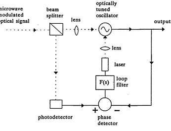
An established technique for phase locking of oscillators at all frequencies is by phase locked loop (PLL). This is basically a feedback control loop which controls the frequency of an oscillator such that its output phase tracks the phase of an injected signal. Optical control of the microwave oscillator can be substituted for the electronic frequency control. Additional components are required, firstly to generate the optical controlling signal, for example a laser or light emitting diode (LED), and secondly to optically couple the light into the oscillator. The proposed loop is shown in Fig 1.2. Other components of the loop are unchanged. The advantages rest entirely in the relative merits of optical tuning compared to electrical frequency control. Important parameters requiring consideration are the maximum optical tuning range, the optical tuning modulation bandwidth, tuning sensitivity and linearity; all of which impact on the performance of the phase locking system. Phase locked loops using optical frequency modulation have not received much attention, and this is reflected in the current lack of information referring to the characterisation of optical frequency tuning effects.
Optical injection locking offers another method of phase locking by purely optical means. This approach differs fundamentally from the PLL above in that locking occurs to an optical signal. Therefore it is more useful for applications in which the locking signal received is in the optical domain already. The locking is a fundamental optical control function and therefore no further components are necessary. Compared to the PLL approach, locking is achieved conveniently and simply.
1.2.2 Optical phase and frequency control
CHAPTER 1
injected signal. The phase error is dependent on the ratio of the frequency difference between the injected signal and the free running oscillation frequency, and the injection locking range. Following Adler [22] it can be expressed in the form;
1 [ü>£ - wJ
L
J
- sin -I 1.1
where is the static phase error, and u>^ are the angular frequencies of the oscillator and injected signal, and is the optical injection locking range.
Frequency control of the oscillator is achieved by changing the injected signal frequency. Phase control is achieved by using the optical frequency tuning sensitivity to tune the oscillator free running frequency and therefore change the static phase error according to Equation 1.1. Phase control by this method has been demonstrated in the optical phase modulation at 500 kHz with 78.8° peak- peak phase variation of a 7.2 GHz MESFET oscillator [23]. The oscillator phase was controlled by varying the mean intensity of the optical injection locking signal.
The system can be converted to operate with closed loop control of the phase by sensing the phase error and feeding back to the frequency tuned oscillator Fig 1.3. The resulting system can be considered from two perspectives. From the point of view of injection locking, the feedback path, which operates as a phase locked loop, stabilises the system by reducing drift in the oscillator free running frequency. It also enables the injection locked oscillator to track frequency variations in the injected signal.
An alternative perspective considers the system as fundamentally a phase locked loop employing optical frequency modulation but with an additional link resulting in simultaneous injection locking. The injection locking effect provides a wideband gain in addition to the gain of the PLL and therefore can be used in the system design to reduce the requirement for the latter.
phase loo p d e te c to r filter in put
F(s)
optically tu n e d
laser lens oscillator o u tp u t
Fig 1.2 Oscillator phase locking by phase locked loop employing optical frequency control.
microwave m odulated optical signal
beam
optically tu n ed oscillator splitter
lens o u tp u t
>
-laser
loop filter F(s)
p h o to d e te c to r phase detector
CHAPTER 1 7
1 3 P h a s e l o c k e d o s c i l l a t o r o p t i c a l r e c e i v e r s
Optically phase locked microwave oscillators can be used for the reception of microwave intensity modulated optical signals. Conventional reception methods employ photodiodes to convert to the electrical domain and subsequent electronic amplification. The phase locked oscillator acts as a photoreceiver with high narrowband gain and high output power. It therefore not only replaces the photodiode but also a large number of amplification stages, Fig 1.4.
As discussed above, an important application for optically phase locked oscillator receivers is in phased array antennas. Phased array antenna design has tended towards so-called active systems in which active solid state devices, located at the elements in the array aperture, provide the power to the transmit beam and amplification to the receive signals prior to summation. The microwave signals required to correlate the phase of the signals at the elements across the aperture can be distributed by optical fibre network. Therefore it is necessary to receive the microwave optical signals with high phase accuracy at each element of the array. The simplification offered to microwave optical signal reception by direct optical phase locking is highly desirable to the phased array anteima as this has the potential to substantially reduce system costs.
Conceptually optical injection locking is the simplest method of phase locking a microwave oscillator to an optical signal. Consequently this has attracted most attention. Direct optical injection locking in microwave oscillators has been demonstrated in IMPATT [28], MESFET [29], HEMT [30] HBT oscillators [31]. The simultaneous direct optical injection locking of two MESFET oscillators also has been demonstrated [16]. Indirect injection locking has been studied for the reception role [17]. However, indirect injection locking is performed by conversion from an optical to an electrical signal by photodiode and then electrical injection into the oscillator circuit. As such injection locking is not optical - the locked oscillator is used simply as a very high gain narrowband amplifier.
(a)
microwave m odulated optical signal
optically tu n ed oscillator
< s >
o u tp u t
— ►
(b)
microwave m odulated
optical signal o u tp u t
PIN diode and low noise front-end amplifier
cascaded gain stages
Fig 1.4 Alternative methods of microwave modulated optical signal reception: (a) by optically phase locked oscillator; (b) by photodetection
CHAPTER 1 9
Closed loop systems such as the phase locked loop, and the combined optical injection locking and phase locked loop system, have the ability to reduce the static phase error to zero. The application of conventional phase locked loops to phased arrays and, in particular, the use of phase locked solid-state microwave sources to obtain high power gain with few active devices was considered by Austin [32]. Wideband loops for high speed acquisition intended for pulsed operation in phased arrays also have been developed [33]. As a result, the optical techniques and closed loop optical phase locking schemes discussed above are appropriate for optical signal reception.
1.4 C o n t e n t s
The present work sets out to consider the three optical phase locking systems from both an analytical and an experimental perspective. The results enable a comparative assessment of the practical application of the three phase locking systems. The application of the phase locking systems to the reception of microwave optical signals, specifically in phased array antennas, will be considered and compared to the alternative conventional techniques.
Chapter 2 reviews the techniques for optical control of microwave oscillator circuits. The principal mechanisms causing the optical control effects are explained and the relative sensitivity of the optical control effects to the control signal magnitude discussed. The scope of the review covers the optical control functions of amplitude modulation, frequency modulation and injection locking. Oscillator control by both direct and indirect optical control are discussed. Direct optical control is performed by direct illumination of the active device in the oscillator circuit: examples of control in both two and three-terminal devices are described. Indirect control is achieved by incorporating a discrete photosensitive component into the oscillator circuit.
Chapter 3 presents an analytical model for the three phase locking systems introduced in Section 1.2. The analysis is presented in general terms and therefore is appropriate for systems employing both optical and electrical control techniques. The model is based on small signal phase locked loop analysis and enables direct comparison of the systems and also a convenient means of system design. In addition practical differences which distinguish the three systems are discussed.
phase lock loop. Chapter 4 concentrates on characterisation of the photoeffect and optical control functions. TTie results of the characterisation are compared to other published examples. Effort is made to identify the principal mechanisms in action, particularly in affecting the oscillator frequency control.
Chapter 5 describes experiments investigating the optical phase locking systems. The systems are assembled using the details of the control function characterisation in Chapter 4. The results firstly confirm the validity of the analytical model of Chapter 3 and secondly demonstrate practical effects predicted involving delay effects and stability conditions.
Chapters 6 and 7 consider the practicalities of optical phase locking systems. Chapter 6 considers the three systems separately, drawing comparisons where possible. For each a quantitative estimate, based on the review and experimental results, is made considering the available performance under ideal conditions. Then limitations that are likely in practice are discussed qualitatively.
Chapter 7 assesses the use of optically phased locked oscillators as receivers in optical fibre distribution networks specifically appropriated for the phased array antenna application. Phase locked oscillator receivers are considered for the reception of narrow bandwidth high frequency phase reference signals. A link budget calculation is made estimating the maximum number of oscillators that can be phase locked by the various phase locking systems and by a single optical signal transmitter via an optical fibre distribution network. The results are compared to the performance of a conventional receiver using photodetection at a photodiode. The practical aspects of the optically phase locked oscillators and the conventional receivers based on a photodiode and amplifier cascade are then discussed.
C hapter 2
O p t ic a lc o n t r o l o f m ic r o w a v ea n d m il l im e t r ew a v eo s c il l a t o r s
2.1 I n t r o d u c t i o n
Optical control is important in providing an alternative to conventional electrical techniques for the control of high frequency circuitiy. This chapter reviews the techniques for optical control of microwave and millimetre wave oscillator circuits, discussing the mechanisms for the optical control and the performance demonstrated.
The discussion below is divided into two sections, concerned with direct and indirect optical control techniques. Optical control of microwave and millimetre wave oscillators can be performed by direct illumination of the active device in the oscillator circuit. Photon absorption and free carrier generation within the device causes changes in the operation and therefore in the oscillation amplitude and frequency. Similar control effects can be achieved by illumination of other photosensitive components incorporated into the oscillator circuit. This latter method is referred to as indirect control since the active oscillator device is not directly affected.
Chapter 1 discussed the principle optical control functions available for the control of solid state oscillators. Interest is mainly with optical frequency modulation and optical injection locking for phase locking applications. However amplitude modulation is often associated with the illumination effects and so is also considered below.
2.2 D i r e c t OPTICAL CONTROL
A recent book [34] reviews direct optical control and most of the recent publications on the subject. Below, the main points are described with the objective of conveying some feel for the control sensitivity that has been demonstrated, and that which is likely in the future.
2^.1 PhotoefTects and wavelength dependency
Photoeffects in semiconductor devices depend on photon absorption and subsequent electron-hole pair generation. The requirement for an absorption event is that the photon energy must exceed that of the semiconductor bandgap. This introduces some wavelength dependency. The absorption can be characterised by the absorption coefficient a, which is used to express the decay in photon flux density with penetration depth, x:
p ( x ) - p ( 0 ) .e x p [ - a x ] 2 . 1
where p(x) is the optical flux density x. The absorption edge refers to the illumination wavelength corresponding to the band-gap energy. Illumination with a wavelength longer than the absorption edge value will not be absorbed.
Table 2.1 shows the absorption parameters in various semiconductors. For wavelengths of less than 900 nm, most show some absorption. The longer wavelengths at 1.3 pm and
Table 2.1(a)
a absorption coefficient (m*^)
semiconductor 826 nm 1.26 pm 1.55 pm
Si 1.9 X 10*
Ge 4.53 X 10* 8.20 X 10* 4.6 X 10* [351
InP 3.09X 10* —
GaAs 1.1 X 10* — —
Table 2.1(b)
composition Ga^^Ini _ ^ A S y P ^ _ y
X 0 0.16 0.27 0.40 0.47
y 0 0.33 0.60 0.85 1.0
absorption edge 300 K
(pm) [36]
0.92 1.12 1.30 1.55 1.65
CHAPTER 2 13
1.55 /iin are used in optical fibre transmission systems due to their low attenuation in optical fibre. However absorption at these wavelengths is limited to a few GaAs/InP alloys.
2J22 Gunn diode oscillators
Most work on the optical control of Gunn diode oscillators to date has been experimental, with a wide range of effects observed [37,38,39,40]. A theoretical framework describing the photoeffects in a Gunn diode is yet to be developed.
222.1 Frequency tuning and amplitude switching
Illumination was shown to enable oscillation in a normally-off GaAs Gunn diode [37]. The diode was biased just below threshold. On illumination, the optically generated plasma causes a local decrease in electric field strength and this enhances sufficiently the field strength elsewhere to trigger the dipole domain oscillation current. The low-field plasma region also acts as a virtual anode for the domains. The position of the optical focus was observed to determine the oscillation period allowing frequency tuning between 6.7 and 10 GHz. Pulsed illumination with 610 nm wavelength and pulse duration and energy of 3 ps and 1 p j (333 mW peak power) triggered bursts of oscillation from the diode. The burst duration increased with nsing optical pulse e n e r ^ ^ 4 ns duration with optical pulse energ»«iof osTpTanj r^ecr.vei^ . This effect is associated with the finite lifetime of the induced plasma.
2 2 2 2 Trap effects
![Fig 1.1 Optical control of microwave oscillators: (a) optical switching (b) optical frequency tuning, (c) optical injection locking, (after Seeds and de Salles, [44])](https://thumb-us.123doks.com/thumbv2/123dok_us/9158050.1453708/42.595.92.461.235.519/optical-control-microwave-oscillators-switching-frequency-injection-locking.webp)