R E V I E W
Open Access
A review of silicon microfabricated ion traps for
quantum information processing
Dong-Il
“
Dan
”
Cho
1*, Seokjun Hong
1, Minjae Lee
1and Taehyun Kim
2Abstract
Quantum information processing (QIP) has become a hot research topic as evidenced by S. Haroche and D. J. Wineland receiving the Nobel Prize in Physics in 2012. Various MEMS-based microfabrication methods will be a key enabling technology in implementing novel and scalable ion traps for QIP. This paper provides a brief introduction of ion trap devices, and reviews ion traps made using conventional precision machining as well as MEMS-based microfabrication. Then, microfabrication methods for ion traps are explained in detail. Finally, current research issues in microfabricated ion traps are presented. The QIP renders significant new challenges for MEMS, as various QIP technologies are being developed for secure encrypted communication and complex computing applications.
Keywords:Microelectromechanial System (MEMS); Microfabrication; Ion traps; Quantum information processing
(QIP); Quantum computing
Introduction
Quantum information processing (QIP) is a novel infor-mation processing method based on quantum mechanics [1-3], and uses two quantum states in a quantum system as a basic unit of information, instead of two voltage levels in conventional information processing based on electronics. This basic unit is called “qubit”, an abbrevi-ation for quantum bit. The informabbrevi-ation stored in a single qubit exists in a superposition of two quantum states which indicates an arbitrary linear combination of two orthonormal basis. Since a single qubit can occupy ei-ther of two states simultaneously, N qubits can represent 2N states of information. Moreover, using a quantum teleportation process [4], two qubits can provide the same measurement results, regardless of the distance between the qubits. Based on these phenomena in the quantum regime, QIP is expected to achieve noticeable increases in the speed in information processing problems. Therefore, many QIP applications such as quantum com-munication [5-7], quantum computer [8-12], and quantum simulator [13-15] have been proposed and are being actively researched.
For the physical implementation of the qubit, a quantum system which is sufficiently isolated from their surround-ings and can be individually manipulated is required. Individual manipulation means qubits are initializable, controllable and measureable. A single atomic ion confined by a physical platform which is called “ion trap” satisfies the requirements [16-19]. Thus the ion trap has become one of the leading technologies among the various qubit platforms including superconducting circuit [20-22], optical lattice [23,24], nuclear magnetic resonance (NMR) [25,26], and quantum dot [27,28]. The ion trap was initially developed by Wolfgang Paul and Hans Georg Dehmelt who are the co-winners of the Nobel Prize in Physics in 1989. Since Cirac and Zoller have proposed using trapped ions as a physical implementation of qubit [16], the feasibility of ion qubits has been verified through many experiments [19,29,30]. Recently, in 2012, Serge Haroche and David Wineland received the Nobel Prize in Physics owing to the measurement and manipulation of individual quantum systems, using cavity quantum electrodynamics (QED) and ion traps, respectively. There has been several review articles on the subject of quantum information processing [18,31-34].
Although the earlier Paul traps were constructed by conventional precision machining method and careful manual assembling, with the advances in MEMS, recent
* Correspondence:[email protected] 1
ISRC/ASRI, Department of Electrical and Computer Engineering, Seoul National University, Seoul 151-744, Republic of Korea
Full list of author information is available at the end of the article
ion traps are based on silicon microfabrication technologies. The basic principles of ion traps are presented in Types of ion trap section. Then, Development history of Paul trap section discusses a history of the Paul trap, which is the type of ion traps mainly covered in this paper. In MEMS-based microfabrication section, two MEMS microfabrication methods for ion traps are explained. Finally, the current issues and the future development directions of microfabri-cated ion traps are presented in Future directions section.
Types of ion trap
An ion trap is a device which can trap charged particles in space by using electric or electromagnetic fields. Trapping a charged particle with static potential alone is impossible because the static potential (φ) obeys one of Maxwell’s equations ∇2φ
= 0 [35]. Wolfgang Paul used an oscillating electric field together with the static electric field [36], and Hans Georg Dehmelt added a magnetic field to the static electric field to trap a positive ion [37]. The ion traps built by Paul and Dehmelt are called “Paul trap” and “Penning trap”a [38] respectively. In this paper, we cover only the Paul trap, because the Paul trap is currently widely used for QIP applications.
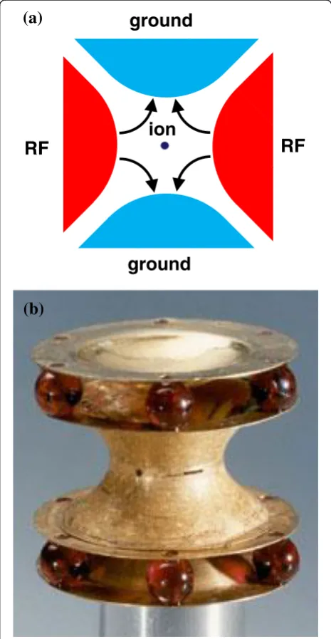
Figure 1(a) shows the structural schematic and trapping principles of the Paul trap, which is composed of a ring-shaped hyperbolic electrode and two endcap electrodes located at the top and bottom of the ring electrode. This type of ion trap is called the“ring trap”compared with the next generation traps which are called the “linear trap” and the“surface trap”. The details of the linear and surface traps are discussed in Development history of Paul trap. Figure 1(b) shows the ring trap made by Wolfgang Paul [39]. In the ring trap, a charged particle is confined in both radial and axial directions by the RF voltage applied to the hyperbolic electrode, and the endcap electrodes function as an RF ground [40]. Typically, the magnitude of the RF voltage is up to hundreds of volts and the frequency of the RF voltage is from tens to hundreds of MHz.
Development history of Paul trap
Ring trap
In the early stages of ion trap researches, the ring type Paul trap was used for experiments concerned in fundamental physics such as frequency standards [41] and mass spectros-copy [42,43]. Ring traps can be easily constructed because of its simple structure, but has a drawback in trapping large numbers of ions because a potential minimum exists at a specific point and difficult to be expanded to a 3-D space.
Linear trap
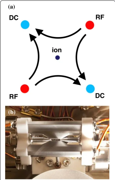
To store more ions, a new ion trap called the “linear trap” was built by Prestage et al. [44]. The first linear trap held approximately 20 times the number of ions as that of a ring trap. Figure 2(a) shows the electrode
structure and electric fields in the radial plane of a linear trap. The hyperbolic electrode of the ring trap is replaced by four rods. Sectors of the circular rods form a hyperbolic shape, and an RF voltage is applied to two opposite rods with the other rods grounded. The pseudopotential gener-ated by the RF voltage confine the ions in the radial direc-tion, and the radial position of the ions is at the center of the four rods. Because the RF null is expanded along the axial direction of the rods, the pseudopotential from the RF voltage cannot confine ions in the axial direction. To
ion
RF
RF
ground
ground
(a)
(b)
confine trapped ions in the axial direction, two endcap electrodes are located at both ends of rod electrodes, and DC voltages are applied to the endcap electrodes to confine the ions axially [45,46].
Cirac and Zoller [16] proposed using trapped ions as a physical implementation of quantum computation. Since then, many research groups have been using linear traps in their QIP experiments. Most of the groups have developed their own linear traps using precision machin-ing and assemblmachin-ing techniques. Each research group has a different electrode structure. Some typical electrode structures include rods [45,47], blades [48,49] and sheets [50]. Figure 2(b) shows a blade type linear trap of the Innsbruck group [48]. Many ion trap research groups are still using a variation of these 4-rod linear traps. In general, when compared to the surface traps (explained in the following sub-section) the 4-rod linear traps have
a higher trap depth, which in turn provide a longer ion life time and more stable trapping of ions. However, the linear traps do not offer the design freedom of the sur-face traps, and currently more research efforts are being expended to the surface traps.
Surface trap
To implement more complicated quantum operations, more ions that can be manipulated in a common motional mode (which refers to the collective oscillation of the whole ion string) should be trapped. Therefore the idea of integrating multiple ion trap arrays in a single ion trap chip was proposed [12,51]. The ion trap chip integrated with multiple ion trap arrays is divided into different regions, as an operation region in which the quantum
Figure 3Schematic and picture of the first ion trap fabricated by a semiconductor fabrication process. (a)Schematic of the ion trap [53].(b)Scanning electron micrograph of the ion trap [53].
RF
RF
DC
DC
ion
(a)
(b)
operations are held, a memory region that stores ions conserving qubit states, and a region for loading ions.
Scalable microfabrication technologies were applied for the implementation of these large scale integrated ion traps, and the first microfabricated ion trap chip imple-mented the 4-rod ion trap configuration using a gallium arsenide (GaAs) based semiconductor fabrication process as shown in Figure 3 [52,53]. In this method, however, the upper and lower electrode layers are separated by an
epitaxially grown aluminium gallium arsenide (AlGaAs) layer, and the vertical distance between the electrodes is limited to a few micrometers whereas the horizontal dis-tance is relatively large at 60 micrometers because of the laser access. This structural asymmetry results in a low ra-dial confinement, which in turn results in a fast ion loss.
To overcome the limitation of implementing a 3-D structure using essentially 2-D fabrication techniques, a breakthrough in the 2-D planar ion trap where all elec-trodes are laid in the same plane was proposed [54-57]. This is more suitable for the silicon-based MEMS micro-fabrication technology. These 2-D ion traps are called the“surface traps”. The surface traps have advantages in the scalability, and are now more widely used by many research groups. Figure 4(a) shows the structure and the principle of the surface trap. All electrodes are fabricated in the same plane. A radial confinement is controlled by two planar RF electrodes, and the position of an RF null where ions are trapped is placed above the two RF elec-trodes. In the 4-rod linear trap, the radial RF null is fixed at the center of the four rods. In the surface trap, the RF null position is above the substrate plane, and the height can be changed as a function of the width of the RF electrodes and the distance between RF electrodes. In most surface trap experiments, the laser path is parallel to the trap surface. For cooling trapped ions by a laser parallel to the trap surface, the principal axis in a radial plane should be rotated. The rotation of principal axis can be realized by varying the widths of the two RF elec-trodes, or by the addition of inner DC electrodes where an asymmetric set of DC voltages is applied to [56,57].
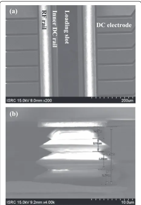
RF RF Outer
DC Inner
DC Outer
DC
ion
Inner DC Loading
slot
(a)
(c)
(b)
Figure 4Schematic and pictures of“surface trap”. (a)Schematic of a surface trap. The red and blue rectangles indicate RF and DC electrodes respectively. The curved arrows denote the direction of electric field when RF voltage is positive. Note that all electrodes are laid on the same plane.(b)Optical image of the surface trap of the Sandia National Laboratory (SNL) group, which has a double metal layer on Si substrate [58].(c)Scanning electron micrograph of the surface trap of the SNL group [59].
Multiple DC electrodes are also fabricated outside the RF electrodes. These outer DC electrode function as the RF ground. By applying different control voltages to these outer DC electrodes, trapped ions can be axially confined. Furthermore, by applying time-varying control voltages to the outer electrodes, the trapped ions can be moved along axis or shuttled.
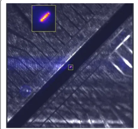
Figure 4(b) and 4(c) show a surface trap developed by the Sandia National Laboratory (SNL) group [58,59], which has a double metal layer on Si substrate [60-62]. The surface trap of the SNL group has been used by many research groups, including those at UC Berkley, Duke University, and Georgia Tech Research Institute through the“Ion Trap Foundry Program”, to successfully demonstrate various quantum experiments [63-65]. We also developed a simi-lar trap chip with optimized shapes, and successfully trapped a string of174Yb+ions as shown in Figure 5 [62]. In Figure 5, a magnified view of the chip layout is also shown. The DC control electrodes are segmented and laid
vertically to the RF rails to generate the axial potentials with an appropriate shape for an axial confinement or a shuttling.
In addition to the Si-based surface traps mentioned in the above, surface traps with a single metal layer on a non-conductive substrate, fabricated by patterning Au electrodes on quartz or sapphire substrates [54,66-69] have been reported. A surface trap has also been fabricated on printed circuit boards [70-72].
MEMS-based microfabrication
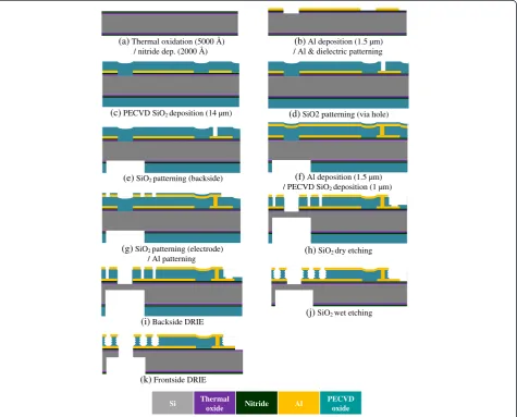
Although many results have been reported on trapping ions with MEMS-fabricated traps, the process details to fabricate the trap chips are very scarce in the literature. Fabricating ion traps requires thick dielectric films to withstand several hundred volts of RF voltages. However, the dielectric layer should be as invisible as possible as seen from the RF null point where ions are trapped, since dielec-tric charging phenomena can alter the null position and can
Si Thermal
oxide Nitride Al
PECVD oxide
(h) SiO2 dry etching
(j) SiO2 wet etching (e) SiO2 patterning (backside)
(g) SiO2 patterning (electrode) / Al patterning
(i) Backside DRIE
(d) SiO2 patterning (via hole) (a) Thermal oxidation (5000 Å)
/ nitride dep. (2000 Å)
(c) PECVD SiO2 deposition (14 µm)
/ PECVD SiO2 deposition (1 µm) (b) Al deposition (1.5 µm) / Al & dielectric patterning
(k) Frontside DRIE
(f) Al deposition (1.5 µm)
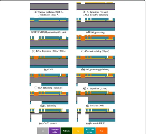
induce the micromotion of trapped ions. In this section, we introduce two fabrication methods developed by us.
The first method is explained in the below. First, a sili-con wafer is cleaned by using the Piranha solution and thermally oxidized to form a 5000-Å SiO2dielectric layer. A 2000-Å silicon nitride film is deposited by a low pres-sure chemical vapor deposition (LPCVD) process to pro-tect the thermal SiO2layer during buffered oxide etching (BOE) at the end of process. These dielectric layers have total thickness of approximately 0.7μm and must be suffi-ciently thick to prevent a breakdown between the bonding pads and the silicon substrate (Figure 6(a)). A 1.5-μm thick aluminum ground layer is deposited on the silicon nitride film by sputtering and dry etched to provide a ground plane for RF shielding and to form wire bonding pads of DC electrodes (Figure 6(b)). A 14-μm thick SiO2 film is deposited by plasma enhanced chemical vapor de-position (PECVD) in several layers to control residual stress (Figure 6(c)). In this case, each SiO2layer is 3–4μm thick and deposited alternately on both sides of the wafer to prevent the residual stress to build up. The PECVD-SiO2 layer on the frontside of the wafer is dry etched to fabricate via holes (Figure 6(d)). After the dry etching of the frontside, the PECVD-SiO2layer on the backside of the wafer is dry etched to provide an oxide hard mask for deep reactive ion etching (DRIE) (Figure 6(e)). In the dry etching process of the 14-μm thick SiO2, the AZ 4620 (Clariant Corporation) photoresist (PR) is used as the etch mask. An additional 1.5-μm thick aluminum layer which is used as electrodes is deposited through a sputtering process (Figure 6(f )). The electrode layer also covers the sidewalls of the etched via holes where the bonding pads and electrodes are electrically connected at. The electrode layer and the PECVD-SiO2layer are patterned and define the electrodes and oxide pillars, respectively (Figure 6(g), (h)). The silicon substrate is etched 450 μm by a DRIE process from the backside of the substrate (Figure 6(i)). The overhang structures are fabricated by the oxide wet etching process using a buffered hydrogen fluoride (BHF) solution (Figure 6(j)). Because the PECVD oxide is depos-ited in several steps, the sidewall profile becomes jagged. The wet etching time must be precisely controlled. Some overhang is required to reduce the dielectric layer expos-ure to the trapped ions, but too large an overhang can result in a long cantilevered top Al layer, which can bend with applied high voltages. After the oxide wet etching process, the slit-shaped ion loading hole is fabricated by a DRIE process, and the fabrication is finished (Figure 6(k)). Figure 7 shows the fabrication results of the ion trap fabricated by this oxide timed etching method described in the above.
This timed etch method is simple but the electrode overhang dimensions are difficult to control. An alterna-tive fabrication method is possible using a sacrificial
material. The fabrication process is the same as the method described in the above up to the step of dry etching the 14-μm thick PECVD-SiO2 (Figure 8(d)). In this study, copper is used as a sacrificial material. The copper technology is selected because it is inexpensive and readily available from the advances in the through silicon via (TSV) technology. A titanium film and a cop-per film are sputtered on the patterned oxide structures, which in turn are utilized as the seed layer for 20-μm copper electroplating (Figure 8(e)). The spaces between the pillars are filled by a copper electroplating process (Figure 8(f)). The electroplated copper and the PECVD-SiO2are planarized by a chemical mechanical polishing (CMP) process (Figure 8(g)). Then, the PECVD-SiO2 layer is dry etched again to fabricate the via holes and the oxide hard mask (Figure 8(h), (i)). An aluminum electrode layer is deposited and dry etched, then the boundaries of the electrodes are defined (Figure 8(j), (k)). In this step, the electrodes patterns are a few micrometers (2 μm in our case) larger than that of the
oxide pillars under the electrodes, and the difference in the pattern sizes determine the length of the overhang structures. After patterning the electrode layer, the sili-con substrate is etched by a DRIE process from the backside (Figure 8(l)). The copper sacrificial layer and the seed layers are removed by a wet etching process (Figure 8(m)). Finally, the fabrication process is com-pleted by penetrating the loading slot through a DRIE process (Figure 8(n)). Figure 9 shows the fabrication re-sults of the copper sacrificial layer method. The vertical sidewalls of oxide pillars are straight (verticality is lim-ited by the dry etching anisotropy of the 14- μm thick SiO2), and the overhang length is controlled to 2μm.
Future directions
Junction ion trap
As discussed in Development history of Paul trap, the num-ber of ion qubits trapped in an ion trap array inevitably must increase in order to adapt more complex quantum algorithms [12]. For trapping and manipulating large num-bers of ions, a multi-zone ion trap composed by a number of ion trap arrays is proposed. In this multi-zone ion trap, the trapping zones are connected by “X” or“Y”junctions, and the information stored in ions can be transferred from one zone to another through the junctions. For shuttling the ions in an axial direction, the location of DC null point is moved along the axial direction by applying
time-dependent potentials to the outer DC control elec-trodes. Ion transports via junctions however require not only applying DC control voltages, but more complex techniques, because pseudopotential barriers created by RF voltages exist near the center of the junctions. Therefore, the geometries near the junctions should be optimized by an iterative algorithm to minimize the magnitude of the pseudopotential barriers.
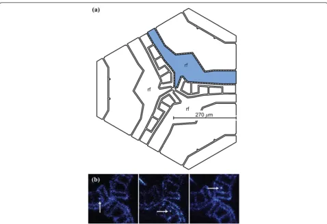
Selective ion transports in junctions have also been demonstrated by a few research groups recently. Hensinger et al.and Blakestadet al. have presented ion transports in T-junction [73] and X-junction [74,75], respectively. The junction ion traps used in these experiments were built by conventional machining methods. Amini et al. [67] and Moehringet al.[76] presented ion transport experiments in Y-junctions. Wright et al. [77] has reported experimental results of ion transports in an X-junction. Figure 10 shows the Y-junction design of the National Institute of Standards and Technology (NIST) group [67]. Figure 10(a) presents an optimized design of RF electrodes at the center of junction and Figure 10(b) shows a charge coupled
Figure 9Scanning electron micrograph of the ion trap fabricated by the copper sacrificial layer method.The vertical sidewall of oxide pillars does not have a jagged edge and 2-μm overhangs are shown.
device (CCD) image of selective ion transports through the Y-junction geometry.
3-D ion trap fabricated by microfabrication technology
Some researchers attempted to develop 3-D ion traps using semiconductor microfabrication processes, because the confining potential of 3-D traps can be much larger and can extend the life time of trapped ions remarkably. For instance, a simulated trap depth of 3-D ion trap fabri-cated by microfabrication is over 10 eV [78] whereas that of surface trap is approximately 0.1 ~ 0.2 eV [59]. The trap depth is the electric potential difference between the potential minimum point and the ion escaping point.
Using a microfabrication process, Wilpers et al. [79,80] have fabricated a 3-D ion trap which has a similar structure to a conventional 4-rod Paul trap. The pseudopotential shape of this microfabricated 3-D ion trap is identical to a 4-rod trap, because the distances between electrodes of the trap in horizontal and vertical directions are equal. Shaikh et al.[81] have developed a 3-D ion trap which has a differ-ent structure from typical 4-rod traps and higher trap depth than surface traps. Figure 11(a) shows a cross section schematic of the 3-D ion trap of National Physical Labora-tory (NPL) group [79]. Figure 11(b) is a scanning electron micrograph (SEM) image of the trap. As mentioned previ-ously, these 3-D traps can provide much larger trap depths.
However, issues concerning a poor laser access and the geometrical complications in achieving ion shuttling need to be addressed.
Conclusion
This paper reviewed the operation principles and the de-velopment history of ion traps. Ion trap has a huge poten-tial to be used in quantum information processing and computing. By applying MEMS-based microfabrication methods as well as conventional machining techniques, various ion traps for QIP experiments have been built and demonstrated. This paper also showed two variations of MEMS fabrication method for surface ion traps. It is ex-pected that the ion trap technology can contribute to realize novel quantum information processing methods with exponential speed-up that we have never experienced so far. It is also expected and anticipated that MEMS fabri-cation technologies will be crucially instrumental in realizing complex yet inexpensive ion traps for quantum information processing and computing.
Endnote
a
Penning trap: The Penning Trap was named after F. M. Penning by Hans Georg Dehmelt because Dehmelt stated getting the inspiration of the trap from the vacuum gauge built by F. M. Penning [38].
Abbreviations
AlGaAs:Aluminum gallium arsenide; NIST: National Institute of Standards and Technology; BHF: Buffered hydrogen fluoride; NMR: Nuclear magnetic resonance; BOE: Buffered oxide etching; NPL: National Physical Laboratory; CCD: Charge coupled device; PECVD: Plasma enhanced chemical vapor deposition; CMP: Chemical mechanical polishing; PR: Photoresist; DRIE: Deep reactive ion etching; QED: Quantum electrodynamics; EMCCD: Electron multiplying charge coupled device; QIP: Quantum information processing; GaAs: Gallium arsenide; SEM: Scanning electron micrograph; LPCVD: Low pressure chemical vapor deposition; SNL: Sandia National Laboratory; MEMS: Microelectromechanical system; TSV: Through silicon via.
Competing interests
The authors declare that they have no competing interests.
Authors’contributions
DC wrote the manuscript. SH and ML surveyed the literature on quantum information processing and microfabricated ion traps. TK surveyed the literature on quantum physics and quantum computing. All authors read and approved the final manuscript.
About the Authors
Dong-il“Dan”Cho(M’88) received the B.S.M.E. degree from Carnegie-Mellon University, Pittsburg, PA, and the S.M. and Ph.D. degrees from the Massachusetts Institute of Technology, Cambridge. From 1987 to 1993, he was an Assistant Professor at Princeton University, Princeton, NJ. Since 1993, he has been with the Department of Electrical and Computer Engineering at Seoul National University, Seoul, Korea, as a Professor, where he is also the Director of the Biomimetic Robot Research Center. His research interests are in microfabrication, bioMEMS, microsensors, and controls. He is the author/coauthor of more than 300 scientific articles in English and the holder/coholder of more than 100 patents. He served as a member of the International Federation of Accountants (IFAC) Technical Board from 2002 to 2005 and as the Vice Chair of the IFAC Technical Board from 2008 to 2014. Since 2014, he is a Council Member of IFAC. He was a founding Editorial Board Member of the IOP Journal of Micromechanics and Microengineering from 1991 to 1996. He has also been an Editor and a Senior
Editor of the IEEE Journal of Microelectromechanical Systems since 1992 to present. He was inducted into the National Academy of Engineering of Korea in 2009, where he currently holds the highest membership level.
Seokjun Hongreceived the B.S. and M.S. degree in the Department of Electrical Engineering from Seoul National University, Korea, in 2009 and 2011 respectively. He is currently pursuing the Ph.D. degree in the Department of Electrical and Computer Engineering at Seoul National University, Korea.
Minjae Leereceived the B.S. degree in the Department of Electrical Engineering from Seoul National University, Korea, in 2011. He is currently pursuing the Ph.D. degree in the Department of Electrical and Computer Engineering at Seoul National University, Korea.
Taehyun Kimreceived the B.S. and M.S. degrees from Seoul National University, Korea, in 1995 and 1997, respectively. He received his Ph.D. degree from Massachusetts Institute of Technology, Cambridge, in 2008. From 2008 to 2011, he was a post-doctoral researcher at Duke University, Durham. In 2011, he joined the Quantum Technology Laboratory of SK Telecom, Korea, where he is currently the project leader.
Acknowledgements
Taehyun Kim was supported by ICT R&D program of MSIP/IITP. [10043464, Development of quantum repeater technology for the application to communication systems].
Author details
1ISRC/ASRI, Department of Electrical and Computer Engineering, Seoul
National University, Seoul 151-744, Republic of Korea.2Quantum Tech. Lab, SK Telecom, Seongnam-si, Republic of Korea.
Received: 12 December 2014 Accepted: 13 January 2015
References
1. Wiesner S (1983) Conjugate coding. ACM Sigact News 15(1):78–88 2. Schumacher B (1995) Quantum coding. Physical Review A 51(4):2738 3. Nielsen MA, Chuang IL (2010) Quantum computation and quantum
information. Cambridge, UK: Cambridge university press
4. Bennett CH, Brassard G, Crépeau C, Jozsa R, Peres A, Wootters WK (1993) Teleporting an unknown quantum state via dual classical and Einstein-Podolsky-Rosen channels. Physical Review Letters 70(13):1895
5. Bennett CH, Brassard G (1984) Quantum cryptography: Public key distribution and coin tossing. In Proceedings of IEEE International Conference on Computers, Systems and. Signal Processing 175(150):8 6. Briegel HJ, Dür W, Cirac JI, Zoller P (1998) Quantum repeaters: The role of imperfect
local operations in quantum communication. Physical Review Letters 81(26):5932 7. Duan LM, Lukin MD, Cirac JI, Zoller P (2001) Long-distance quantum
communication with atomic ensembles and linear optics. Nature 414(6862):413–418
8. Deutsch D, Jozsa R (1992) Rapid solution of problems by quantum computation. In proceedings of the Royal Society of London Series A: Mathematical and Physical Sciences 439(1907):553–558
9. Shor PW (1994) Algorithms for quantum computation: Discrete logarithms and factoring. In proceedings of 35th Annual Symposium on Foundations of Computer Science: 124–134
10. DiVincenzo DP (1995) Quantum computation. Science 270(5234):255–261 11. Jones JA, Mosca M, Hansen RH (1998) Implementation of a quantum search
algorithm on a quantum computer. Nature 393(6683):344–346 12. Kielpinski D, Monroe C, Wineland DJ (2002) Architecture for a large-scale
ion-trap quantum computer. Nature 417(6890):709–711
13. Feynman RP (1982) Simulating physics with computers. International journal of theoretical physics 21(6):467–488
14. Aspuru-Guzik A, Dutoi AD, Love PJ, Head-Gordon M (2005) Simulated quantum computation of molecular energies. Science 309(5741):1704–1707 15. Buluta I, Nori F (2009) Quantum simulators. Science 326(5949):108–111 16. Cirac JI, Zoller P (1995) Quantum computations with cold trapped ions.
Physical review letters 74(20):4091–4094
17. Schmidt-Kaler F, Häffner H, Riebe M, Gulde S, Lancaster GP, Deuschle T, Becher C, Roos CF, Eschner J, Blatt R (2003) Realization of the Cirac–Zoller controlled-NOT quantum gate. Nature 422(6930):408–411
19. Home JP, Hanneke D, Jost JD, Amini JM, Leibfried D, Wineland DJ (2009) Complete methods set for scalable ion trap quantum information processing. Science 325(5945):1227–1230
20. Devoret MH, Schoelkopf RJ (2013) Superconducting circuits for quantum information: an outlook. Science 339(6124):1169–1174
21. Martinis JM, Nam S, Aumentado J, Urbina C (2002) Rabi oscillations in a large Josephson-junction qubit. Physical Review Letters 89(11):117901 22. Clarke J, Wilhelm FK (2008) Superconducting quantum bits. Nature
453(7198):1031–1042
23. Pachos JK, Knight PL (2003) Quantum computation with a one-dimensional optical lattice. Physical review letters 91(10):107902
24. Brennen GK, Caves CM, Jessen PS, Deutsch IH (1999) Quantum logic gates in optical lattices. Physical Review Letters 82(5):1060
25. Gershenfeld NA, Chuang IL (1997) Bulk spin-resonance quantum computation. science, 275(5298): 350–356
26. Vandersypen LM, Chuang IL (2005) NMR techniques for quantum control and computation. Reviews of modern physics 76(4):1037
27. Imamog A, Awschalom DD, Burkard G, DiVincenzo DP, Loss D, Sherwin M, Small A (1999) Quantum information processing using quantum dot spins and cavity QED. Physical Review Letters 83(20):4204
28. Loss D, DiVincenzo DP (1998) Quantum computation with quantum dots. Physical Review A 57(1):120
29. Moehring DL, Maunz P, Olmschenk S, Younge KC, Matsukevich DN, Duan LM, Monroe C (2007) Entanglement of single-atom quantum bits at a distance. Nature 449(7158):68–71
30. Leibfried D, DeMarco B, Meyer V, Lucas D, Barrett M, Britton J, Itano WM, Jelenkovic B, Langer C, Rosenband T, Wineland DJ (2003) Experimental demonstration of a robust, high-fidelity geometric two ion-qubit phase gate. Nature 422(6930):412–415
31. Steane A (1997) The ion trap quantum information processor. Applied Physics B: Lasers and Optics 64(6):623–643
32. Monroe C, Kim J (2013) Scaling the ion trap quantum processor. Science 339(6124):1164–1169
33. Kimble H (2008) The quantum internet. Nature 453(7198):1023–1030 34. Ladd TD, Jelezko F, Laflamme R, Nakamura Y, Monroe C, O’Brien JL (2010)
Quantum computers. Nature 464(7285):45–53
35. Griffiths DJ, Reed College (1999) Introduction to electrodynamics (Vol. 3). Upper Saddle River, NJ: prentice Hall
36. Paul W, Reinhard HP, Zahn U (1959) Das elektrische Massenfilter als Massenspektrometer und Isotopentrenner. Zeitschrift für Physik 152(2):143–182 37. Dehmelt HG (1967) Radiofrequency spectroscopy of stored ions I: Storage.
Adv At Mol Phys 3:53
38. Penning FM, Nienhuis K (1949) Construction and applications of a new design of the Philips vacuum gauge. Philips Technical Review, Netherlands, p 11 39. Webpage of Department of Physics and Astronomy at Bonn University in
2014 [http://bigs.physics-astro.uni-bonn.de/index.php?id=76]
40. March RE (2009) Quadrupole ion traps. Mass spectrometry reviews 28(6):961–989 41. Wineland DJ, Bergquist JC, Bollinger JJ, Itano WM, Heinzen DJ, Gilbert SL,
Manney CH, Raizen MG (1990) Progress at NIST toward absolute frequency standards using stored ions. Ultrasonics, Ferroelectrics and Frequency Control, IEEE Transactions on 37(6):515–523
42. Louris JN, Cooks RG, Syka J, Kelley PE, Stafford GC, Todd JF (1987) Instrumentation, applications, and energy deposition in quadrupole ion-trap tandem mass spectrometry. Analytical Chemistry 59(13):1677–1685 43. Kaiser RE, Graham CR, Stafford GC, Syka JE, Hemberger P (1991) Operation
of a quadrupole ion trap mass spectrometer to achieve high mass/charge ratios. International journal of mass spectrometry and ion processes 106:79–115
44. Prestage JD, Dick GJ, Maleki L (1989) New ion trap for frequency standard applications. Journal of Applied Physics 66(3):1013–1017
45. Raizen MG, Gilligan JM, Bergquist JC, Itano WM, Wineland DJ (1992) Ionic crystals in a linear Paul trap. Physical Review A 45(9):6493
46. Monz T, Schindler P, Barreiro JT, Chwalla M, Nigg D, Coish WA, Harlander M, Hänsel W, Hennrich M, Blatt R (2011) 14-qubit entanglement: Creation and coherence. Physical Review Letters 106(13):130506
47. Nägerl HC (1998) Ion strings for quantum computation. Ph.D dissertation 48. Webpage of Institut für Quantenoptik und Quanteninformation at Innsbruck
[http://heart-c704.uibk.ac.at/index.php/en/research/lintrap]
49. Huber G, Deuschle T, Schnitzler W, Reichle R, Singer K, Schmidt-Kaler F (2008) Transport of ions in a segmented linear Paul trap in printed-circuit-board technology. New Journal of Physics 10(1): 013004
50. Brama E, Mortensen A, Keller M, Lange W (2012) Heating rates in a thin ion trap for microcavity experiments. Applied Physics B 107(4):945–954 51. Cirac JI, Zoller P (2000) A scalable quantum computer with ions in an array
of microtraps. Nature 404(6778):579–581
52. Madsen MJ, Hensinger WK, Stick D, Rabchuk JA, Monroe C (2004) Planar ion trap geometry for microfabrication. Applied Physics B 78(5):639–651 53. Stick D, Hensinger WK, Olmschenk S, Madsen MJ, Schwab K, Monroe C
(2005) Ion trap in a semiconductor chip. Nature Physics 2(1):36–39 54. Seidelin S, Chiaverini J, Reichle R, Bollinger JJ, Leibfried D, Britton J, Wesenberg
JH, Blakestad RB, Epstein RJ, Hume DB, Jost JD, Langer C, Ozeri R, Shiga N, Wineland DJ (2006) Microfabricated surface-electrode ion trap for scalable quantum information processing. Physical review letters 96(25):253003 55. Wesenberg JH (2008) Electrostatics of surface-electrode ion traps. Physical
Review A 78(6):063410
56. Reichel J, Vuletic V (2010) Atom chips, Hoboken, NJ: John Wiley & Sons 57. Hughes MD, Lekitsch B, Broersma JA, Hensinger WK (2011) Microfabricated
ion traps. Contemporary Physics 52(6):505–529
58. Stajic J (2013) The future of quantum information processing. Science 339(6124):1163–1163
59. Stick D, Fortier KM, Haltli R, Highstrete C, Moehring DL, Tigges C, Blain MG (2010) Demonstration of a microfabricated surface electrode ion trap. arXiv preprint arXiv:1008.0990
60. Leibrandt DR, Labaziewicz J, Clark RF, Chuang IL, Epstein RJ, Ospelkaus C, Wesenberg JH, Bollinger JJ, Leibfried D, Wineland DJ, Stick D, Sterk J, Monroe C, Pai CS, Low Y, Frahm R, Slusher RE (2009) Demonstration of a scalable, multiplexed ion trap for quantum information processing. Quantum Information & Computation 9(11):901–919
61. Merrill JT, Volin C, Landgren D, Amini JM, Wright K, Doret SC, Pai CS, Hayden H, Killian T, Faircloth D, Brown KR, Harter AW, Slusher RE (2011) Demonstration of integrated microscale optics in surface-electrode ion traps. New Journal of Physics 13(10):103005
62. Kim T, Yoon J, Ahn J, Kim M, Kim J, Choi D, Hong S, Lee M, and Cho, D (2013) Development of quantum repeater based on ion trap. The 4th International Quantum Optics Workshop
63. Ramm M, Pruttivarasin T, Häffner H (2013) Energy Transport in Trapped Ion Chains. arXiv preprint arXiv:1312.5786
64. Mount E, Baek SY, Blain M, Stick D, Gaultney D, Crain S, Noek R, Kim T, Maunz P, Kim J (2013) Single qubit manipulation in a microfabricated surface electrode ion trap. New Journal of Physics 15(9):093018 65. Shu G, Vittorini G, Buikema A, Nichols CS, Volin C, Stick D, Brown KR (2014)
Heating rates and ion-motion control in a Y-junction surface-electrode trap. Physical Review A 89(6):062308
66. Allcock DTC, Sherman JA, Stacey DN, Burrell AH, Curtis MJ, Imreh G, Linke NM, Szwer DJ, Webster SC, Steane AM, Lucas DM (2010) Implementation of a symmetric surface-electrode ion trap with field compensation using a modulated Raman effect. New Journal of Physics 12(5):053026
67. Amini JM, Uys H, Wesenberg JH, Seidelin S, Britton J, Bollinger JJ, Leibfried D, Ospelkaus C, VanDevender AP, Wineland DJ (2010) Toward scalable ion traps for quantum information processing. New journal of Physics 12(3):033031 68. Tanaka U, Suzuki K, Ibaraki Y, Urabe S (2014) Design of a surface electrode
trap for parallel ion strings. Journal of Physics B: Atomic, Molecular and Optical Physics, 47(3):035301
69. Noek R, Kim T, Mount E, Baek SY, Maunz P, Kim J (2013) Trapping and cooling of 174Yb + ions in a microfabricated surface trap. Journal of the Korean Physical Society 63(4):907–913
70. Brown KR, Clark RJ, Labaziewicz J, Richerme P, Leibrandt DR, Chuang IL (2007) Loading and characterization of a printed-circuit-board atomic ion trap. Physical Review A 75(1):015401
71. Li X, Jiang G, Luo C, Xu F, Wang Y, Ding L, Ding CF (2009) Ion trap array mass analyzer: structure and performance. Analytical chemistry 81(12):4840–4846 72. Kim TH, Herskind PF, Kim T, Kim J, Chuang IL (2010) Surface-electrode point
Paul trap. Physical Review A 82(4):043412
73. Hensinger WK, Olmschenk S, Stick D, Hucul D, Yeo M, Acton M, Deslauriers L, Monroe C, Rabchuk J (2006) T-junction ion trap array for two-dimensional ion shuttling, storage, and manipulation. Appl Phys Lett 88(3):034101 74. Blakestad RB, Ospelkaus C, VanDevender AP, Amini JM, Britton J, Leibfried D,
Wineland DJ (2009) High-Fidelity Transport of Trapped-Ion Qubits through an X-Junction Trap Array. Phys Rev Lett 102(15):153002
76. Moehring DL, Highstrete C, Stick D, Fortier KM, Haltli R, Tigges C, Blain MG (2011) Design, fabrication and experimental demonstration of junction surface ion traps. New Journal of Physics 13(7):075018
77. Wright K, Amini JM, Faircloth DL, Volin C, Doret SC, Hayden H, Pai CS, Landgren DW, Denison D, Killian T, Slusher RE, Harter AW (2013) Reliable transport through a microfabricated X-junction surface-electrode ion trap. New Journal of Physics 15(3):033004
78. Brownnutt M, Wilpers G, Gill P, Thompson RC, Sinclair AG (2006) Monolithic microfabricated ion trap chip design for scaleable quantum processors. New Journal of Physics 8(10):232
79. Wilpers G, See P, Gill P, Sinclair AG (2012) A monolithic array of three-dimensional ion traps fabricated with conventional semiconductor technology. Nature nanotechnology 7(9):572–576
80. See P, Wilpers G, Gill P, Sinclair AG (2013) Fabrication of a Monolithic Array of Three Dimensional Si-based Ion Traps. Journal of Microelectromechanical System 22(5):1180–1189
81. Shaikh F, Ozakin A, Amini JM, Hayden H, Pai CS, Volin C, Denison DR, Faircloth D, Harter AW, Slusher RE (2011) Monolithic Microfabricated Symmetric Ion Trap for Quantum Information Processing. arXiv preprint arXiv:1105.4909
Submit your manuscript to a
journal and benefi t from:
7Convenient online submission
7Rigorous peer review
7Immediate publication on acceptance
7Open access: articles freely available online
7High visibility within the fi eld
7Retaining the copyright to your article
![Figure 11 Schematic and picture of microfabricated 3-D ion trap of National Physical Laboratory (NPL) group [79]](https://thumb-us.123doks.com/thumbv2/123dok_us/888697.1586284/9.595.60.538.255.708/figure-schematic-picture-microfabricated-national-physical-laboratory-group.webp)
