Diffusion-Driven Charge Transport in Light Emitting
Devices
Iurii Kim1,*ID, Pyry Kivisaari2, Jani Oksanen2and Sami Suihkonen1
1 Department of Electronics and Nanoengineering, Aalto University, P.O. Box 13500, 00076 Aalto, Finland
2 Engineered Nanosystems Group, Aalto University, P.O. Box 12200, 00076 Aalto, Finland
* Correspondence: [email protected]; Tel.: +358-41-369-8162
Abstract: Almost all modern inorganic light-emitting diode (LED) designs are based on double heterojunctions (DHJs) whose structure and current injection principle have remained essentially unchanged for decades. Although highly efficient devices based on the DHJ design have been developed and commercialized for energy-efficient general lighting, the conventional DHJ design requires burying the active region (AR) inside a pn-junction. This has hindered the development of emitters utilizing nanostructured ARs located close to device surfaces such as nanowires or surface quantum wells. Modern DHJ III-N LEDs also exhibit resistive losses which arise from the DHJ device geometry. The recently introduced diffusion-driven charge transport (DDCT) emitter design offers a novel way to transport charge carriers to unconventionally placed ARs. In a DDCT device, the AR is located apart from the pn-junction and the charge carriers are injected into the AR by bipolar diffusion. This device design allows the integration of surface ARs to semiconductor LEDs and offers a promising method to reduce resistive losses in high power devices. In this work, we present a review of the recent progress in gallium nitride (GaN) based DDCT devices, and an outlook of potential DDCT has for opto- and microelectronics.
Keywords: light-emitting diodes (LEDs); diffusion injection; lateral epitaxial overgrowth; selective-area growth (SAG)
1. Introduction
The electrically driven double heterojunction (DHJ) sandwiching an active material layer between the p- and n-type charge injection layers is nowadays so ubiquitous in semiconductor industry that it is almost impossible to imagine any viable options for it [1,2]. Particularly, all laser diodes and highly effective light-emitting diodes (LEDs) [3], as well as many heterostructure bipolar transistors [4], field effect transistors [5], and state-of-the-art solar cells [6] use DHJs whose function has remained essentially similar for decades. All of these structures traditionally realize the current transport by using the conventional DHJ-like configuration where the active region, e.g., quantum well (QW) or multi-quantum well (MQW) stack, is located between n- and p-doped semiconductor regions and the electrons and holes enter the active region from the opposite directions. In the case of LEDs, biasing the LED generates a drift current transporting carriers into the opposite edges of the depletion region. The charge carriers are further transported and spread in the active region by diffusion. This configuration satisfies the needs of most LED structures for general lighting. Nevertheless, conventional LEDs still come across with some technological and power efficiency challenges especially in high-power lighting applications [2,7].
Sandwiching the AR between the n- and p-type regions is straightforward with modern fabrication processes, but imposes limits on the device geometries that can be realized without effort [8,9]. Moreover, utilizing modern materials such as nanowires (NW), quantum-dots (QDs), surface plasmon enhanced and 2D-materials for the active region is both interesting for research and promising to enhance LED performance. However, the complications arising from the LED design based on the DHJ model are a significant bottleneck for utilizing such new materials [10–12]. For example, around 40 years passed since the invention of the nanowire growth mechanism [13] before the first NW based
LED was fabricated [14–16]. If DHJ is used, the NW must have contacts on both ends to enable an electrical path through the nanowire, and thus contact fabrication for NWs becomes challenging due to the long and complicated process. In addition, the deposition of top contact, in general, absorbs the light emitted by any materials listed above decreasing the efficiency of the LED.
From the III-nitride LED point of view in particular, the phenomenon called ”efficiency droop” is assessed as one of the most prominent scientific and technological challenges [17]. In the droop-effect an increasing injection current leads to significant drop off in the emission efficiency of blue LEDs with indium gallium nitride (InGaN) MQW active layers [18–20]. The mechanisms of the efficiency droop in InGaN LEDs have been studied extensively, where carrier delocalization [21–23] and electron leakage [18,24] are proposed to be key reasons, while the most recent reports mainly pointing to Auger recombination as the main culprit [25–28]. Secondly, particularly in the modern high quantum efficiency LEDs, the efficiency droop limitations, current crowding and resistive loss become the most severe bottlenecks for high output power devices, confining their optimal high-efficiency performance at current densities well below 100 A/cm2[29–34].
Diffusion-driven charge transport (DDCT) has been recently developed as a possible alternative current injection method in order to avoid DHJ limitations [35,36], originally with the aim to enable efficient current spreading over large area light emitters for electroluminescent cooling devices such as thermophotonic heat pumps [37]. In contrast with conventional DHJ, in the DDCT scheme the AR is located outside the pn-junction, and both carrier types (electrons and holes) diffuse to the AR through at least partly overlapping paths. Following the originally computational introduction of the DDCT scheme, the III-nitride diffusion injected light emitting diode (DILED) [38–40] and surface InGaN QW located on top of gallium nitride (GaN) pn-homojunction (S-LED) [41] have been fabricated and characterized. It has been demonstrated that the obtained devices lean on the mechanism of carrier diffusion to the QW/MQW excited through one of its interfaces only. In addition, simulations suggest that the efficiency of DDCT devices based on lateral heterojunctions (LHJ) [42] can also exceed the efficiency of comparable DHJ structures. Consequently, the DDCT scheme can offer new possibilities for high-power lighting applications as well as several emerging devices making use of nanowires, 2D materials, quantum dots, plasmonic and near field phenomena. In this study, we review the recent progress in light-emitting diodes based on diffusion-driven charge transport. We also discuss the outlook for using DDCT to electrically excite new promising materials such as monolayers and quantum dots.
2. First Demonstrations of Diffusion-Driven Charge Transport
2.1. Basics of the DDCT Concept
In principle, conventional electrical excitation of LEDs as well as the structures mentioned above are based on an AR sandwiched in a pn-junction. When the LED is biased, the transport of majority carriers mainly takes place as a drift current due to a small electric field transporting the carriers from the n- and p-type regions towards the depletion region. Starting from the edge of the depletion region, the main component of the net current, on the other hand, is diffusion. Therefore, typical LEDs essentially behave as 1D structures where diffusion transports electrons and holes to the AR from p-and n-type regions located at opposite sides of the AR. However, the minority carrier diffusion may extend over relatively long distances even in the presence of the DHJ potential barriers. This represents a main disadvantage for conventional devices, so far as diffusion of electrons over the MQW results in carrier leakage and decreases the device efficiency. In contrast, DDCT-based devices take advantage of such diffusion currents.
diffusing carriers so that combining these two allows electrical excitation of ARs located outside the pn-junction. In Ref. [35] we presented numerical solutions of current transport equations for freestanding nanowire emitter structures based on III-N semiconductors shown in Figure1. It was suggested that bipolar diffusion injection works with both minority electrons and minority holes, by a comparing two different variations where the thin bulk region immediately below the nanowires was either p- or n-type.
a) b)
Figure 1.(a) Schematic illustration of the free-standing n-type (p-type) nanowire emitter structures studied in Ref. [35] (b) The 2-dimensional lateral cross section model of the structure and dimensions as they are used in the calculations of the reference. Note that the figures are not in scale. Reproduced from [35], with the permission of cAIP Publishing 2013.
The ultimate requirement to make use of DDCT is that the AR is located within the diffusion length of carriers (electrons or holes) from the pn-junction. This will enable a diffusion path for minority carriers between the pn-junction and the AR. As an example, in Ref. [35], the structure simulated under a 3.5 V bias resulted in substantial electron/hole densities in the NWs. Specifically in the structure with p-GaN below the NWs, the electron concentration was small in the p-type region and large in the NWs, resulting from efficient diffusion of electrons through the p-type region from the pn-junction. Similar effect was obtained for the reverse structure where diffusion injection worked with minority holes. Moreover it was shown that due to large electron and hole concentrations in the NWs, almost all recombination took place there. These results suggested that the bipolar diffusion injection concept can be used to inject free-standing nanowire structures, and they encouraged us to test the idea experimentally, first with planar GaN LEDs with InGaN QWs.
2.2. Theory and Equivalent Circuit
The basic features of DDCT can be explained using standard semiconductor transport models summarized e.g. in Ref. [42]. For illustration purposes, in Ref. [39] we also developed an equivalent circuit model to study how the diffusion current to the AR and the loss currents depend on the structure details, and how the current to the AR can be enhanced. Here we summarize the model for the structure shown in Figure2(a) with its equivalent circuit shown in Figure2(b). The device consists essentially of the pn-junction in the GaN host material and the lower-bandgap InGaN AR, both of which can be modelled as parallel diodes with their separate diode laws. If the host material has a relatively low number of defects, the pn-junction current consists primarily of carrier diffusion to the contacts, which can be approximated with the short diode law given by
Ipn =qn2i
D
nAp NaLp
+DpAn
NdLn exp
qV
pn kBT
−1
, (1)
AR pn
Rs
pn AR p-GaN
n-GaN InGaN
a) b)
Figure 2. (a) Simplified sketch of one of the structures studied in Ref. [35] and (b) its equivalent circuit model. The equivalent circuit has two parallel diodes describing leakage current to the contacts (labelled ”pn”) and current to the AR. The resistanceRsdescribes resistive losses in the homogeneous regions of the device.
ionized donor and acceptor densities,Ln,pare the distances between the pjunction edge and the n-and p-type contacts,Vpnis the voltage applied over the pn-junction,kBis Boltzmann’s constant, andT is the temperature.
When the device includes a low-bandgap AR outside the pn-junction as in Figure2, recombination in the AR forms a somewhat similar current sink as the carrier loss taking place at the two contacts which resulted in Eq. (1). In the device of Figure2, there is always a large density of electrons next to the AR, and recombination in the AR is therefore limited by the availability of holes. In this case, holes can diffuse from the pn-junction to the AR similarly as when they diffuse towards the n-contact, and this hole diffusion can be approximated with a diode law reminiscent of Eq. (1), given by
IAR =qn2i DpAAR
NdLAR
exp
qV
pn kBT
−1
, (2)
whereAARis the cross-section area of theARandLARis the distance between the pn-junction edge and the AR. Comparing Eqs. (1) and (2), it can be seen that IAR can be increased without increasingIpne.g. by extending the cross-section area of the AR and decreasing the distance between the AR and the pn-junction edge. If most of the pn junction current consists of electron leakage as is usually the case with GaN,IARcan even be enhanced by decreasingNd. On the other hand, increasing temperature is expected to enhance the operation of the structure in Figure2partly by increasingDp and, in the case of GaN, more importantly by enhancing acceptor activation and hence the number of holes available for diffusion. In the context of Eq. (2), the increasing acceptor activation decreasesLAR, as the depletion region extends further to the n-side and its edge therefore moves closer to the AR. On the other hand, in Section3we analyze devices that can enhanceIAR significantly further by using lateral doping techniques.
2.3. Diffusion Injected Buried MQW LED (DILED)
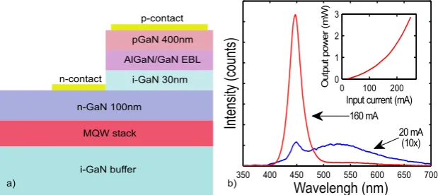
As the first experimental verification of DDCT concept, in Ref. [38] we reported the first buried multi-quantum well light-emitting diode structure injected by the bipolar diffusion. The fabricated device contained a MQW stack located below the GaN pn-junction as schematically illustrated in Figure 3(a). The device structure was based around the conventional III-nitride LED fabrication processes and utilized the same metal-organic chemical vapor deposition (MOCVD) growth, lithography, etching and contacting steps. The MQW stack was placed under the n- and p-doped regions in order to avoid the magnesium (Mg) memory effect [43,44] in MOCVD and to avoid a dry etching of the p-doped layer. The electrically excited sample showed a strong blue emission at room temperature at 450nm wavelength with 160 mA injection current, corresponding to the emission from the InGaN AR. With low excitation power (20mA), also yellow luminescence was observed and identified to result from defects in the unintentionally doped GaN (i-GaN) spacer between the p- and n-GaN. However, since the QWs were located outside the pn-junction, blue emission confirmed that both electrons and holes were transported to the QWs from the same side of the active region through bipolar diffusion. Secondary electron-hole generation in the MQW due to UV light emission from the pn-junction was ruled out as there was no trace of band-edge luminescence from the pn-junction in the spectrum (Figure3(b)), meaning that the excitation level in the pn-junction was still weak.
Figure3(b) shows the measured optical output power of the sample as a function of the injection current. As can be seen from the figure the output power of the DILED increased superlinearly with increasing input current. This exceptional behavior, i.e., no effect from efficiency droop at high injection currents was explained by a low carrier concentration in the active region, so that the LED did not yet enter the droop regime.
a) 350 400 450 500 550 600 650 700
160 mA 20 mA
(10x)
0 100 200
0 1 2 3
O
u
tp
u
t
p
o
w
e
r
(m
W
)
Input current (mA)
p-contact
n-contact
i-GaN buffer MQW stack
b) n-GaN 100nm
i-GaN 30nm AlGaN/GaN EBL
pGaN 400nm
Wavelengh (nm)
Intensity (counts)
Figure 3.(a) Schematic illustration of the layer structure and thicknesses. The InGaN/GaN MQW stack is located under both p- and n-layers and thus outside the pn-junction. (b) Spectra of the studied DILED at injection currents of 20mA and 160mA measured at room temperature. The intensity of the 20mA measurement is scaled by a factor of 10 in order to show the lineshape of the spectrum. The measured optical power as a function of input current is shown in the inset. Reproduced from [38], with the permission of cAIP Publishing 2014.
that bipolar diffusion can not only excite the QW nearest to a pn-junction, but also to transport both electrons and holes over the potential barriers of a MQW stack.
The presented structures were the first experimental demonstration that bipolar diffusion can transport electrons and holes into the active region located outside the pn-junction and a proof of the diffusion-driven charge transport concept. This device configuration was designed to demonstrate the basic operating principle of diffusion injection by modifying a conventional III-nitride LED fabrication processes. The efficiency of the device was fairly low, but simulations suggest that relatively simple methods can be used to significantly increase the efficiency of the DILED structure by modifying its geometry and doping levels, bringing the injection efficiency even close to unity [39]. However, the structure shown in Figure3did not completely exclude the possibility of an alternative current path, as electrons enter the intrinsic GaN below the MQW and enter the MQW from the bottom side below the p-contact.
2.4. Diffusion-Driven Surface QW LED (S-LED)
While the diffusion injected buried MQW LED described in the previous chapter was the first experimental demonstration of a DDCT-based LED, it had very little novel device functionality. The further development of DDCT-based devices had a double motivation. On the one hand, the goal was to eliminate all parallel non-diffusion based current paths, and on the other hand to demonstrate the novel possibilities enabled by the DDCT-structure. The current diffusion-driven charge transport model can be applied to solve design challenges related to emitters based on near surface quantum wells, surface NWs, QDs, and layered 2D emitting materials, which are hard-to-reach with conventional DHJ structures. With help of DDCT, such emitters can be excited electrically through the bottom contact only with no need for top contacts. This will allow integration of nano-scale surface light emitters in applications which are impossible to realize with DHJ. Moreover, a device with a surface AR leaves out all other electrical excitation mechanisms except bipolar diffusion through only one side of the AR.
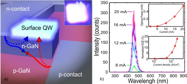
To pursue these goals our group recently demonstrated the diffusion injection excitation for near surface light-emitting structures [41]. The fabricated S-LED is illustrated in Figure4(a) and contains an InGaN QW located on top of a GaN pn-junction. Such design is leaving the light-emitting surface entirely free of metals or other contact structures. The electrically excited charge carriers from the pn-homojunction are transported to the near surface QW by the bipolar diffusion as indicated by arrows in Figure4(a). In addition, the structure does not enable any alternative charge transport paths to the AR than bipolar diffusion from the same side of the AR.
Surface QW n-contact p-contact n-GaN p-GaN a) 300 0
400 500 600 700 800 900
50 100 150 200 250 300 350 0.4 0.2
0 5 10 15 20
0 5 10 15 20 102 103 20 mA 16 mA 12 mA 8 mA Optical Pow er (m W) Current (mA) Norm alized EQE (%)
Current density (A/cm )2
Wavelengh (nm)
Intensity (counts)
b)
As in the DILED structure of the previous subsection, the light emission from the S-LED is made possible by functionally separating the pn-junction which initially creates the excitation and the near surface QW where the radiative recombination takes place. In suitably engineered structures, the carriers injected into the p- and n-layers are efficiently transported to the near surface QW by bipolar diffusion through the bottom interface of the QW only. Therefore, there is no carrier flux through the top interface of the QW and the net current through any horizontal cross-section of the QW is always zero as in optical pumping. However, in contrast to direct optical pumping, the demonstrated electrical excitation method does not directly generate carriers in the surface quantum well, but all the carriers instead enter the QW through bipolar diffusion.
Conclusive proof of the diffusion current injection was observed in the emission spectrum of the electrically driven device (Figure4(b)). As in the case of the buried QW device in the previous subsection, the intense light emission from the InGaN QW and the absence of any band-to-band UV emission from the GaN layers clearly showed that the charge carriers were transported to the QW through its bottom interface by diffusion. Moreover, strong blue emission was easily observed by a naked eye at room temperature (inset of Figure4(a)). The external quantum efficiency (EQE) of S-LED is approximately one fifth of the efficiency of a reference single QW InGaN/GaN DHJ device at room temperature shown in the inset of Figure4(b). This corresponds to an optical power of 0.5 mW from the 30 x 30µm QW mesa at 20 mA operating current as demonstrated on the second inset of Figure
4(b).
The S-LED clearly shows that a surface QW can be excited by carrier diffusion through the bottom interface of the QW only. As the first demonstration of an electrically injected near surface QW, the S-LED provides the conclusive evidence of its feasibility for exciting surface nanostructures.
3. Laterally Doped DDCT Devices
All structures mentioned above as well as the associated theory and simulations were built on a vertically formed pn-homojunction. Presented devices demonstrated the first experimental verification of the DDCT concept and its potential to solve different design challenges in conventional LEDs. Nonetheless, the vertically formed pn-homojunction model involves potential barriers and leads to electrical inefficiencies which do not fully support reducing the effects of current crowding, resistive losses and efficiency drop.
3.1. Lateral Heterojunction (LHJ) Concept
n-contact p-contact
n-GaN p-GaN i-GaN or InGaN/GaN
InGaN QW Buffer
a) b)
n-contact p-contact
n-GaN
p-GaN
i-GaN or InGaN/GaN
InGaN QW Buffer
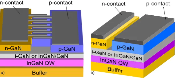
Figure 5.Schematic illustration of the LHJ LED finger structure based on III-N materials. (a) Perspective image of ne chip device, (b) fingers side view. Figure (b) reproduced from [42], with the permission of
c
Wiley-VCH Verlag GmbH & Co. KGaA. Publishing 2017.
overgrown GaN layers fabricated e.g. with selective area regrowth. We presented the first steps towards the realization of such planar design in Ref. [42,45]. Simulations suggested that electrical inefficiencies and sub-optimal device performance observed in previous studies can be eliminated by adapting the DDCT concept in laterally doped heterojunction (LHJ) structures. Figure5shows a schematic illustration of LHJ structure, where narrow n- and p-doped regions are fabricated side by side, so that electrons and holes can flow to the continuous AR through bipolar diffusion. Such structures can be realized using either selective area growth (SAG) or ion-implantation techniques. Our simulations show that current crowding can almost be eliminated by using the LHJ structure and that it is possible to reduce the resistive heating of the devices by further improvements using suitable material composition gradings.
3.2. Realization of LHJ using Ion Implantation
The conventional approach to realize laterally doped structures e.g. in silicon industry is ion implantation. However, ion implantation doping in GaN is challenging due to several reasons. First of all, the ionization energy of the implanted materials in GaN is considerably large and thereby results in low activation efficiency [46,47]. Secondly, relatively high temperatures are typically required to achieve activation of both n- and p-type implanted dopants [48,49]. Moreover, ion implantation technique inflicts damage to the GaN lattice and damage removal is not straightforward [49]. Nevertheless, the possibility of creating a n-GaN layer on p-type GaN with reasonable carrier concentration 5×1019cm−3has been demonstrated when Si-implanted p-type GaN was annealed in N2ambience [47].
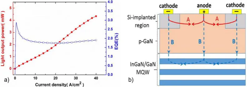
Despite the challenges associated with ion implantation, a device structure based on a lateral GaN pn-junction was introduced very recently by Lee et al. [50]. They demonstrated a laterally doped GaN-based light-emitting diode with the InGaN/GaN QWs placed under a lateral array of GaN pn-homojunctions shown in6(b). In the figure A and B denote the current paths of drift and diffusion current, respectively. Patterned n-doped regions were formed using selective-area Si implantation onto a MOCVD grown p-GaN cap layer followed by thermal annealing in N2. The resulting lateral
heterojunction structure was utilized to serve as a carrier injector for the planar InGaN/GaN MQW stack placed underneath the p-GaN.
a) b)
Figure 6.(a) Typical current density-dependent light output power and EQEs. (b) Schematic of the current paths in the LEDs. The separation between the contacts of the structure is approximately 50µm.
Reproduced from [50], with the permission of cIEEE Publishing 2017.
The advantage of the ion implantation doped structure is the ability to form selectively doped lateral pn-junctions without a dry etching procedure which can chemically alter the GaN surface and make the fabrication of ohmic contacts more challenging [51]. In the considered implanted structure, a heavily Si-doped n+-InGaN top layer was created on the p-GaN layer. After Si-ion implantation with 1×1016cm−2dosage and 70 keV energy, the implanted Si ions distributed an average depth of approximately 60 nm from the top surface layer. Annealing samples at 1000◦C in N2ambient activates
the implanted Si ions in the p-GaN layer and converts p-GaN layer with a hole concentration of 3×
1017cm−3into n-GaN layer with sheet electron concentration of 3×1014cm−2[50].
3.3. Selective Area Growth as a Method to Realize a Lateral Pn-junction
In addition to ion implantation, also selective area growth (SAG) can be used to fabricate patterned areas of semiconductor material. The SAG of arsenide and phosphide III-V materials has been analyzed quite extensively and utilized as a major method for nanowire growth [52–54]. In III-N technology, SAG has been employed mostly in epitaxial lateral overgrowth (ELOG) methods which were developed to reduce threading dislocations in heteroepitaxial growth [55–57]. In contrast with ion implantation, the extensively characterized [58–62] defect-free GaN layers grown by lateral epitaxial over-growth can provide a more beneficial solution to realize LHJ structures [63].
For the SAG of p- and n-type GaN layers needed to fabricate the structure shown in Figure5we utilized a 6×2" Aixtron close-coupled showerhead MOCVD system. Trimethylgallium (TMGa), trimethylaluminum (TMAl), and trimethylindium (TMIn) were used as precursors for gallium, aluminum, and indium, respectively. Ammonia (NH3) was used as a precursor for the nitrogen
(N2). Disilane (Si2H6) and bis(cyclopentadienyl)magnesium (Cp2Mg) were used for n- and p-type
doping respectively. The carrier concentrations of the layers at room temperature were 2×1017cm−3, 5×1018 cm−3, and 5×1016cm−3for p-GaN, n-GaN, and i-GaN, respectively. All structures were fabricated on 2-inch c-Al2O3wafers with a 5µm unintentionally doped GaN buffer layer, followed by
a standard 5 well InGaN/GaN MQW active region and a 120 nm i-GaN capping layer. These template structures were then used as substrates for studying the n-GaN and p-GaN SAG processes. The SAG mask was fabricated by standard lithography techniques and a SiO2layer deposited by PECVD. The
mask openings fingers and spacings in SiO2growth mask were varied from 2µm to 20µm. The n-type
Buffer
InGaN QW
i-GaN
SiO2 SiO2
Resist Resist
SiO2 n-GaN
SiO
2 n-GaNSiO
2n-GaN n-GaN SiO2 SiO2
Resist Resist
n-GaN n-GaN
Resist Resist
n-GaN n-GaN p-GaN p-GaN
Buffer
InGaN QW
i-GaN
Buffer
InGaN QW
i-GaN
Buffer
InGaN QW
i-GaN
Buffer
InGaN QW
i-GaN
Buffer
InGaN QW
i-GaN
a)b) 2 um 10 um
Figure 7. (a) The main steps of the LHJ LED fabrication process. (b)Typical SEM images of SAG grown n-GaN fingers showing the effect of chemical patterning residues on growth (left) as well as the properly grown fingers (right).
The epitaxial overgrowth requires a proper cleaning step of the top layer from the resist residue or SiO2residue in mask openings. An ill-prepared sample can lead to not well-faceted growth, threading
dislocations or non-uniform growth as shown on the left image in Figure7(b). These defects have no significant influence on luminescence from optical pumping, but for electrically excited samples they could dramatically increase the electrical resistance of the interfaces. An interesting feature of SAG in submillimeter scale is given by the different vertical and lateral overgrowth rates in mask openings. However, these strong geometrical effects can be controlled with pattern mask geometry [64].
300nm b)
2.160um
25um a)
p-GaN
before regrowth
n-GaN
before SAG
100µm
Wavelengh (nm)
Intensity (counts)
c) 4000
3000
2000
1000
0
525 500 475 450 425
In Refs. [42,45] we showed first results from structure with separately grown n- and p-GaN regions shown on Figure8(a) and (b). Fig.8(a) shows the n-type layer (mesa and fingers on the left) and an opening in the SiO2mask made for the p-GaN region (mesa and fingers on the right). Figure
8(b) shows an SEM image from the circled area in (a) for a structure where the SAG of both the n- and p-type GaN regions has been completed and the SiO2mask has been removed. Figure8(c) further
shows the PL from the samples excited using a pump laser at 405 nm before and after SAG of p- and n-type GaN. Based on the PL measurements SAG does not notably affect the luminescence of the MQW, suggesting that SAG provides a promising method to fabricate laterally doped GaN devices.
Simulations presented in the papers [42,45] compare the lateral current spreading and current crowding properties of high power GaN LEDs based on conventional DHJ structures and structures based on the DDCT principle. As a result, we showed that using a single-side graded active region both facilitates the current transport in the LHJ device and leads to only a modest efficiency droop by increasing the effective thickness of the active region. Moreover, comparing the operation of the LHJ structure with conventional LEDs and an ideal vertical LED showed that the LHJ structure shows practically no added differential resistance or efficiency loss due to lateral current crowding.
4. Outlook of DDCT-Based LEDs
The main difference between the DDCT-structure and the conventional DHJ-structure is that in the DDCT-structure the AR is not sandwiched inside a pn-junction. Instead, the structure is designed so that the AR is completely separate from the pn-junction and located within the diffusion length of carriers (at most a few to a few tens of microns in absence of potential barriers) from the junction. The spatial and functional separation of the pn-junction and the AR enable a fundamentally different starting point for device design, and therefore enables very different solutions to carrier injection to a semiconductor surface than what is available using DHJ. The DDCT-scheme can be thought to provide a new and general method to transport carriers to or from the surface and adjacent materials. The main requirement for the method is that the AR can act as a carrier drain or source, which then induces the diffusion current. Therefore the band-gap of the surface emitter generally needs to be smaller and the carrier life time shorter than in the pn-diode material. In this review article we concentrated on DDCT of GaN LEDs. However, the DDCT model is in principle equally applicable for any other materials and light-emitting/absorbing devices. A particularly interesting possibility is to fabricate the pn-junction from an indirect band gap material (such as Si) which then excites a light emitting AR on the device surface.
Using the DDCT-scheme, emitters based on e.g. near surface QWs, surface NWs, QDs and ML emitting materials can be fabricated without top contacts as shown in Figure1. III-N-based NWs grown on low cost, large-area substrates hold promises in applications in solid state lighting and full-color displays [65], and InAs and InP NWs grown on Si as near infra-red emitters [66]. Emission wavelengths ranging from UV to near-infrared have been demonstrated using GaN-based NW heterostructures, where small diameter InN-NWs are considered as one candidate technology which can bridge the “green gap” [67]. Additionally, room temperature phosphor-free white-light emission in the mW range
has been realized by GaN nanowire LEDs [68].
5. Summary
Breaking free of the strict and long-lived limitation to sandwich the active region within a pn-junction provides new possibilities for the design and development of emerging next generation optoelectronic devices. Here we have reviewed the brief history of the concept of diffusion driven charge transport, which holds the promise of fully separating the functionality of sourcing and draining electron-hole pairs in semiconductors by allowing spatial separation of the pn-junction and the active region. While the fundamental possibility of DDCT is easily visible from the diffusion terms of the basic semiconductor transport equations, its technological relevance is much more difficult to assess. In this article, we have reviewed several technologically relevant demonstrations of the concept in various light emitting structures, most notably the buried AR light emitting diode, surface AR LED and the laterally doped DDCT LED. We also briefly discussed the outlook of using DDCT in developing new free-standing nanowire LEDs and other emerging possibilities enabled by DDCT.
In order to gain further technological traction, however, the next development steps of the concept will involve both studying the possibility to optimize the presently introduced structures as well as to demonstrating entirely new approaches to realize e.g. applications involving NWs or nanoplasmonics. If the predictions of the simulations carried out on the DDCT structures this far turn out to be reliable, the deployment of the DDCT concept could lead to dramatic improvements in the ability to harness the emerging nanomaterials for practical applications.
Acknowledgments:The authors acknowledge the financial support from the Nokia Foundation, Emil Aaltonen Foundation and Walter Ahlström Foundation (PK), the Academy of Finland [projects 297916 (SS), 297853, 307142, 310567 (JO)], European research Council [project 638173 (JO)] and Aalto energy platform. Part of the research was performed at the OtaNano — Micronova Nanofabrication center of Aalto University.
References
1. Alferov, Z.I. Nobel Lecture: The double heterostructure concept and its applications in physics, electronics, and technology.Reviews of Modern Physics2001,73, 767–782.
2. Nakamura, S.; Krames, M.R. History of gallium-nitride-based light-emitting diodes for illumination.
Proceedings of the IEEE2013,101, 2211–2220.
3. Nakamura, S. Background story of the invention of efficient blue InGaN light emitting diodes (Nobel Lecture). Annalen der Physik2015,527, 335–349.
4. Alferov, Z. Heterostructures for optoelectronics: History and modern trends.Proceedings of the IEEE2013,
101, 2176–2182.
5. Hou, H.W.; Liu, Z.; Teng, J.H.; Palacios, T.; Chua, S.J. High Temperature Terahertz Detectors Realized by a GaN High Electron Mobility Transistor. Scientific Reports2017,7, 46664.
6. Arif, M.; Elhuni, W.; Streque, J.; Sundaram, S.; Belahsene, S.; El Gmili, Y.; Jordan, M.; Li, X.; Patriarche, G.; Slaoui, A.; Migan, A.; Abderrahim, R.; Djebbour, Z.; Voss, P.L.; Salvestrini, J.P.; Ougazzaden, A. Improving InGaN heterojunction solar cells efficiency using a semibulk absorber. Solar Energy Materials and Solar Cells 2017,159, 405–411.
7. Steranka, F.M.; Bhat, J.; Collins, D.; Cook, L.; Craford, M.G.; Fletcher, R.; Gardner, N.; Grillot, P.; Goetz, W.; Keuper, M.; Khare, R.; Kim, A.; Krames, M.; Harbers, G.; Ludowise, M.; Martin, P.S.; Misra, M.; Mueller, G.; Mueller-Mach, R.; Rudaz, S.; Shen, Y.C.; Steigerwald, D.; Stockman, S.; Subramanya, S.; Trottier, T.; Wierer, J.J. High power LEDs - Technology status and market applications. Physica Status Solidi (A) Applied Research2002,194, 380–388.
8. Schubert, E.F.Light-Emitting Diodes; 2006; pp. 201–221.
9. Parrilla, M.; Newson, D.; Skellern, D.; MacBean, M. Modeling, design and performance of InP/InGaAs double-heterojunction bipolar transistors. LEOS 1992 Summer Topical Meeting Digest on Broadband Analog and Digital Optoelectronics, Optical Multiple Access Networks, Integrated Optoelectronics, and Smart Pixels. IEEE, 1992, pp. 414–417.
10. Homeyer, E.; Mattila, P.; Oksanen, J.; Sadi, T.; Nykänen, H.; Suihkonen, S.; Symonds, C.; Tulkki, J.; Tuomisto, F.; Sopanen, M.; Bellessa, J. Enhanced light extraction from InGaN/GaN quantum wells with silver gratings.
11. Sadaf, S.M.; Ra, Y.H.; Nguyen, H.P.T.; Djavid, M.; Mi, Z. Alternating-Current InGaN/GaN Tunnel Junction Nanowire White-Light Emitting Diodes.Nano Letters2015,15, 6696–6701.
12. Jones, E.A.; Wang, F.F.; Costinett, D. Review of Commercial GaN Power Devices and GaN-Based Converter Design Challenges. IEEE Journal of Emerging and Selected Topics in Power Electronics2016,4, 707–719. 13. Wagner, R.S.; Ellis, W.C. Vapor-Liquid-Solid Mechanism of Single Crystal Growth.Applied Physics Letters
1964,4, 89–90.
14. Duan, X.; Lieber, C.M. Laser-Assisted Catalytic Growth of Single Crystal GaN Nanowires. Journal of the American Chemical Society2000,122, 188–189.
15. Chen, C.C.; Yeh, C.C. Large-Scale Catalytic Synthesis of Crystalline Gallium Nitride Nanowires. Advanced Materials2000,12, 738–741.
16. Lieber, C.M. Semiconductor nanowires: A platform for nanoscience and nanotechnology. 2010 3rd International Nanoelectronics Conference (INEC). IEEE, 2010, pp. 5–6.
17. Piprek, J. Efficiency droop in nitride-based light-emitting diodes.Physica Status Solidi (A) Applications and Materials Science2010,207, 2217–2225.
18. Verzellesi, G.; Saguatti, D.; Meneghini, M.; Bertazzi, F.; Goano, M.; Meneghesso, G.; Zanoni, E. Efficiency droop in InGaN/GaN blue light-emitting diodes: Physical mechanisms and remedies. Journal of Applied Physics2013,114.
19. Feng, M.X.; Sun, Q.; Liu, J.P.; Li, Z.C.; Zhou, Y.; Zhang, S.M.; Yang, H. A Study of Efficiency Droop Phenomenon in GaN-Based Laser Diodes before Lasing.Materials2017,10, 482.
20. Ryu, H.Y.; Jeon, K.S.; Kang, M.G.; Yuh, H.K.; Choi, Y.H.; Lee, J.S. A comparative study of efficiency droop and internal electric field for InGaN blue lighting-emitting diodes on silicon and sapphire substrates.
Scientific Reports2017,7, 44814.
21. Hammersley, S.; Watson-Parris, D.; Dawson, P.; Godfrey, M.J.; Badcock, T.J.; Kappers, M.J.; McAleese, C.; Oliver, R.A.; Humphreys, C.J. The consequences of high injected carrier densities on carrier localization and efficiency droop in InGaN/GaN quantum well structures. Journal of Applied Physics2012,111, 083512. 22. Bochkareva, N.I.; Rebane, Y.T.; Shreter, Y.G. Efficiency droop in GaN LEDs at high current densities: Tunneling leakage currents and incomplete lateral carrier localization in InGaN/GaN quantum wells.
Semiconductors2014,48, 1079–1087.
23. Mickeviˇcius, J.; Podlipskas, Ž.; Aleksiej ¯unas, R.; Kadys, A.; Jurkeviˇcius, J.; Tamulaitis, G.; Shur, M.S.; Shatalov, M.; Yang, J.; Gaska, R. Nonradiative Recombination, Carrier Localization, and Emission Efficiency of AlGaN Epilayers with Different Al Content. Journal of Electronic Materials2015,44, 4706–4709.
24. Kivisaari, P.; Berg, A.; Karimi, M.; Storm, K.; Limpert, S.; Oksanen, J.; Samuelson, L.; Pettersson, H.; Borgström, M.T. Optimization of Current Injection in AlGaInP Core-Shell Nanowire Light-Emitting Diodes.
Nano Letters2017,17, 3599–3606.
25. Brendel, M.; Kruse, A.; Jönen, H.; Hoffmann, L.; Bremers, H.; Rossow, U.; Hangleiter, A. Auger recombination in GaInN/GaN quantum well laser structures. Applied Physics Letters2011,99, 031106. 26. Iveland, J.; Martinelli, L.; Peretti, J.; Speck, J.S.; Weisbuch, C. Direct measurement of Auger electrons
emitted from a semiconductor light-emitting diode under electrical injection: identification of the dominant mechanism for efficiency droop. Physical review letters2013,110, 177406,[1304.5469].
27. Tian, P.; McKendry, J.J.D.; Herrnsdorf, J.; Watson, S.; Ferreira, R.; Watson, I.M.; Gu, E.; Kelly, A.E.; Dawson, M.D. Temperature-dependent efficiency droop of blue InGaN micro-light emitting diodes. Applied Physics Letters2014,105.
28. Kivisaari, P.; Sadi, T.; Li, J.; Rinke, P.; Oksanen, J. On the Monte Carlo Description of Hot Carrier Effects and Device Characteristics of III-N LEDs. Advanced Electronic Materials2017,3, 1600494.
29. Kim, H.; Park, S.J.; Hwang, H.; Park, N.M. Lateral current transport path, a model for GaN-based light-emitting diodes: Applications to practical device designs. Applied Physics Letters2002,81, 1326–1328. 30. Shaw, J.L.; Treece, R.E.; Patel, D.; Menoni, C.S.; Smith, J.R.; Pankove, J.I. Electron emission from GaN n–p
junctions.Applied Physics Letters2002,81, 3076–3078.
31. Balakrishnan, K.; Katona, T.; Khan, A. Ultraviolet light-emitting diodes based on group three nitrides.
Nature Photonics2008,2, 77–84.
33. Chang, K.S.; Yang, S.C.; Kim, J.Y.; Kook, M.H.; Ryu, S.Y.; Choi, H.Y.; Kim, G.H. Precise temperature mapping of GaN-based LEDs by quantitative infrared micro-thermography.Sensors (Basel, Switzerland) 2012,12, 4648–60.
34. Wu, P.C.; Ou, S.L.; Horng, R.H.; Wuu, D.S. Improved Performance of High-Voltage Vertical GaN LEDs via Modification of Micro-Cell Geometry.Applied Sciences2017,7, 506.
35. Kivisaari, P.; Oksanen, J.; Tulkki, J. Current injection to free-standing III-N nanowires by bipolar diffusion.
Applied Physics Letters2013,103, 031103.
36. Kivisaari, P.; Oksanen, J.; Tulkki, J. Diffusion-assisted current spreading for III-nitride light-emitting applications. SPIE Proceedings2013,8625, 862528.
37. Oksanen, J.; Tulkki, J. Thermophotonic heat pump—a theoretical model and numerical simulations. Journal of Applied Physics2010,107, 093106.
38. Riuttanen, L.; Kivisaari, P.; Nykänen, H.; Svensk, O.; Suihkonen, S.; Oksanen, J.; Tulkki, J.; Sopanen, M. Diffusion injected multi-quantum well light-emitting diode structure. Applied Physics Letters2014,
104, 081102.
39. Riuttanen, L.; Kivisaari, P.; Svensk, O.; Oksanen, J.; Suihkonen, S. Diffusion Injection in a Buried Multiquantum Well Light-Emitting Diode Structure.IEEE Transactions on Electron Devices2015,62, 902–908. 40. Riuttanen, L.; Kivisaari, P.; Svensk, O.; Vasara, T.; Myllys, P.; Oksanen, J.; Suihkonen, S. Vertical excitation profile in diffusion injected multi-quantum well light emitting diode structure. SPIE Proceedings; Chyi, J.I.; Fujioka, H.; Morkoç, H., Eds., 2015, p. 93632A.
41. Riuttanen, L.; Kivisaari, P.; Svensk, O.; Oksanen, J.; Suihkonen, S. Electrical injection to contactless near-surface InGaN quantum well. Applied Physics Letters2015,107, 051106.
42. Kivisaari, P.; Kim, I.; Suihkonen, S.; Oksanen, J. Elimination of Lateral Resistance and Current Crowding in Large-Area LEDs by Composition Grading and Diffusion-Driven Charge Transport. Advanced Electronic Materials2017,3, 1700103.
43. Xing, H.; Green, D.S.; Yu, H.; Mates, T.; Kozodoy, P.; Keller, S.; Denbaars, S.P.; Mishra, U.K. Memory effect and redistribution of Mg into sequentially regrown GaN layer by metalorganic chemical vapor deposition.
Japanese Journal of Applied Physics, Part 1: Regular Papers and Short Notes and Review Papers2003,42, 50–53. 44. Lee, S.N.; Paek, H.S.; Son, J.K.; Kim, H.; Kim, K.K.; Ha, K.H.; Nam, O.H.; Park, Y. Effects of Mg dopant on
the degradation of InGaN multiple quantum wells in AlInGaN-based light emitting devices. Journal of Electroceramics2009,23, 406–409.
45. Kivisaari, P.; Kim, I.; Suihkonen, S.; Oksanen, J. Elimination of resistive losses in large-area LEDs by new diffusion-driven devices. SPIE Proceedings; Kim, J.K.; Krames, M.R.; Tu, L.W.; Strassburg, M., Eds., 2017, Vol. 1, p. 101240Z.
46. Edgar, J.Properties of Group III Nitrides; INSPEC, 1994; p. 310.
47. Sheu, J.K.; Tun, C.J.; Tsai, M.S.; Lee, C.C.; Chi, G.C.; Chang, S.J.; Su, Y.K. n+-GaN formed by Si implantation into p -GaN.Journal of Applied Physics2002,91, 1845–1848.
48. Zolper, J.C.; Wilson, R.G.; Pearton, S.J.; Stall, R.A. Ca and O ion implantation doping of GaN. Applied Physics Letters1996,68, 1945–1947.
49. Tan, H.H.; Williams, J.S.; Zou, J.; Cockayne, D.J.H.; Pearton, S.J.; Stall, R.A. Damage to epitaxial GaN layers by silicon implantation.Applied Physics Letters1996,69, 2364–2366.
50. Lee, M.l.; Yeh, Y.h.; Liu, Z.y.; Chiang, K.j.; Sheu, J.k. Planar GaN-Based Blue Light-Emitting Diodes With Surface p-n Junction Formed by Selective-Area Si–Ion Implantation. IEEE Transactions on Electron Devices 2017,64, 4156–4160.
51. Ping, A.T.; Chen, Q.; Yang, J.W.; Khan, M.A.; Adesida, I. The effects of reactive ion etching-induced damage on the characteristics of ohmic contacts to n-type GaN.Journal of Electronic Materials1998,27, 261–265. 52. Tomioka, K.; Ikejiri, K.; Tanaka, T.; Motohisa, J.; Hara, S.; Hiruma, K.; Fukui, T. Selective-area growth of
III-V nanowires and their applications. Journal of Materials Research2011,26, 2127–2141.
53. Choi, K.; Arita, M.; Arakawa, Y. Selective-area growth of thin GaN nanowires by MOCVD. Journal of Crystal Growth2012,357, 58–61.
54. Ito, T.; Akiyama, T. Recent Progress in Computational Materials Science for Semiconductor Epitaxial Growth. Crystals2017,7, 46.
56. Suihkonen, S.; Ali, M.; Svensk, O.; Sintonen, S.; Sopanen, M.; Lipsanen, H.; Törmä, P.T.; Nevedomsky, V.; Bert, N. Patterning of sapphire/GaN substrates. Physica Status Solidi (C)2011,8, 1509–1512.
57. Zhou, S.; Wang, H.; Lin, Z.; Yang, H.; Hong, X.; Li, G. Study of defects in LED epitaxial layers grown on the optimized hemispherical patterned sapphire substrates.Japanese Journal of Applied Physics2014,53, 025503. 58. Nam, O.h.; Bremser, M.D.; Zheleva, T.S.; Davis, R.F. Lateral epitaxy of low defect density GaN layers via
organometallic vapor phase epitaxy. Applied Physics Letters1997,71, 2638–2640.
59. Hiramatsu, K.; Nishiyama, K.; Motogaito, A.; Miyake, H.; Iyechika, Y.; Maeda, T. Recent Progress in Selective Area Growth and Epitaxial Lateral Overgrowth of III-Nitrides: Effects of Reactor Pressure in MOVPE Growth. physica status solidi (a)1999,176, 535–543.
60. Beaumont, B.; Vennegues, P.; Gibart, P. Epitaxial Lateral Overgrowth of GaN.physica status solidi (b)2001,
227, 1–43.
61. Gibart, P. Metal organic vapour phase epitaxy of GaN and lateral overgrowth.Reports on Progress in Physics 2004,67, 667–715.
62. Wang, T. Topical Review: Development of overgrown semi-polar GaN for high efficiency green/yellow emission. Semiconductor Science and Technology2016,31, 093003.
63. Ronning, C. Ion implantation into gallium nitride.Physics Reports2001,351, 349–385.
64. Tanaka, A.; Chen, R.; Jungjohann, K.L.; Dayeh, S.A. Strong Geometrical Effects in Submillimeter Selective Area Growth and Light Extraction of GaN Light Emitting Diodes on Sapphire. Scientific Reports2015,
5, 17314.
65. Nguyen, H.P.T.; Djavid, M.; Cui, K.; Mi, Z. Temperature-dependent nonradiative recombination processes in GaN-based nanowire white-light-emitting diodes on silicon. Nanotechnology2012,23, 194012.
66. Chen, R.; Tran, T.T.D.; Ng, K.W.; Ko, W.S.; Chuang, L.C.; Sedgwick, F.G.; Chang-Hasnain, C. Nanolasers grown on silicon.Nature Photonics2011,5, 170–175,[1101.3305].
67. Bayerl, D.; Kioupakis, E. Visible-Wavelength Polarized-Light Emission with Small-Diameter InN Nanowires.Nano Letters2014,14, 3709–3714.
68. Nguyen, H.P.T.; Zhang, S.; Connie, A.T.; Kibria, M.G.; Wang, Q.; Shih, I.; Mi, Z. Breaking the Carrier Injection Bottleneck of Phosphor-Free Nanowire White Light-Emitting Diodes. Nano Letters2013,