Int. J. Nanosci. Nanotechnol., Vol. 13, No. 1, March. 2017, pp. 53-58
Design of Optimized Quantum-dot Cellular
Automata RS Flip Flops
A. Rezaei*
1 Electrical Engineering Department, Kermanshah University of Technology, Kermanshah,
Iran
(*) Corresponding author: [email protected], [email protected] (Received: 13 April 2015 and Accepted: 02 October 2016)
Abstract
Complementary metal-oxide semiconductor (CMOS) technology has been the industry standard to implement Very Large Scale Integrated (VLSI) devices for the last two decades. Due to the consequences of miniaturization of such devices (i.e. increasing switching speeds, increasing complexity and decreasing power consumption), it is essential to replace them with a new technology. Quantum-dot cellular automata (QCA) is one of the alternative technologies proposed as a replacement solution to the fundamental limits of CMOS technology. QCA has the potential to be one of the features promising nanotechnologies because of its higher speed, smaller size and lower power consumption in comparison with transistor-based technology. This work proposes optimized QCA RS (Reset Set) flip flops. The proposed structures are simulated and validated using QCADesigner software. In comparison with the previous works the proposed QCA RS flip flops require the minimum number of cells, area and delay. Also, in comparison with CMOS technology our QCA designs are more efficient in terms of area, delay and frequency. Therefore, these structures can be used to design nanoscale circuits.
Keywords:Quantum-dot Cellular Automata, Majority Gate, QCADesigner, RS Flip Flop. 1. INRODUCTION
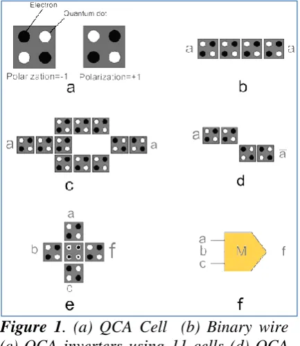
In the last few decades, scaling in feature size and increase in processing power have been achieved by conventional CMOS technology. Due to basic physical limitations, the conventional VLSI technology faces serious challenging problems in feature size reduction. In contrast, relying on unique properties of the electronic devices at nanoscale sizes, nanotechnology opens new horizons for systems and devices. Among these new devices, Quantum-dot Cellular Automata (QCA) [1, 2] relies on new physical phenomena, and innovative techniques that radically depart from a CMOS-based model. In QCA, the digital information is processed using polarization rather than current. In QCA, binary information is stored as the position of individual electrons (a bi-stable charge configuration) [3]. The fundamental unit of the QCA is the QCA cell. The QCA cell created with four quantum dots (a position, in which a
c . b c . a b . a ) c , b , a ( M
f (1)
Majority gate can be realized by 5 QCA cells, as shown in Fig. 1e [4]. Logic AND and OR Gates can be implemented using the majority Gate as follow:
) 0 , b , a ( M b .
a (2) ) 1 , b , a ( M b
a (3)
The circuit diagram of the majority Gate is shown in Fig. 1f.
Figure 1. (a) QCA Cell (b) Binary wire (c) QCA inverters using 11 cells (d) QCA inverters using 4 cells (e) QCA implementation of majority Gate (f) Circuit diagram of majority Gate.
The circuits in QCA technology require a clock to control and synchronize the information flow and also to provide the power to run the circuit. Unlike CMOS technology, which its clock pulse consists of an upper phase and a lower phase, the QCA clock pulse has four phases: switch, release, hold and rest, which are represented as shown in the Fig. 2. In the switch phase, QCA cell is influenced by its neighbors and its polarization settles down to one of the two ground polarization states. In the hold phase, the cell is latched to its current polarization state. In the release phase, the cell starts to lose its polarization. In the relax phase, the
electrons are free to tunnel and delocalize themselves. The QCA cell polarization is determined when it is in the switch phase by the polarization of its neighboring cells, which are at the switch or hold phase.
Figure 2. QCA clocking.
less area. Also, they work with less clock phases.
2. RS FLIP FLOP DESIGN
The Boolean expression for an RS flip flop is given by:
n 1
n S R.Q
Q (4)
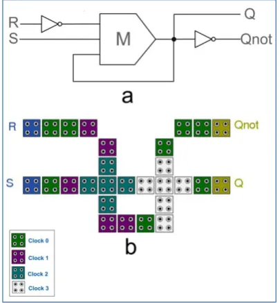
The block diagram of the QCA RS flip flop is shown in Fig. 3a [6]. This block diagram is equivalent to the following equation [6]:
) Q , R , S ( M
Qn1 n (5)
Fig.3b shows the first proposed QCA RS flip flop layout. The inner loop of the flip flop has a delay of one clock cycle; therefore at the output, Q is available 5 clocking zones after R and S have been applied. Fig.4 shows the second proposed RF flip flop. In this layout, the inner loop of the flip flop has a delay of one clock cycle; but at the output, Q is available 4 clocking zones after R and S have been applied.
Figure 3. The first proposed QCA RS flip flop (a): Schematic diagram (b) QCA layout.
The proposed structure in Fig. 3b is verified using QCADesigner ver.2.0.3 [14], with the following parameters for a bistable approximation [14]: Cell
size=18nm, Number of samples=20000, Radius of effect=90nm, Relative
permittivity=12.9, Convergence
tolerance=0.001, Clock high=9.8e-22J, Clock low=3.8e-23J, Clock amplitude factor =2, Layer separation=11.5nm and Maximum Iterations per sample =100.
Figure 4. Layout of the second proposed QCA RS flip flop.
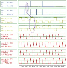
3. RESULTS AND DISCUSSIONS Fig.5 and Fig.6 show the fault free simulation results for the proposed QCA RS flip flops. The second proposed structure (Fig.4) is verified using QCADesigner ver.2.0.3 [14], with the following parameters used for a bistable approximation: Cell size=18 nm, Number of samples=12800, Radius of effect=65nm, Relative permittivity=12.9, Convergence tolerance=0.00001, Clock high=9.8e-22J, Clock low=3.8e-23J, Clock amplitude factor =2, Layer separation=11.5nm and Maximum Iterations per sample =1000. Table 1 compares the proposed RS flip flops with the previous works presented in [6, 15-17]. As it is seen from Table 1, in comparison with the previous work presented in [6] the optimization rate (OT) (sometime called “Percentage Reduction”) for the first proposed design is 70 % and 60 % in the area and cell count, respectively. Also it is faster. The OT is obtained using the following equation:
100 * Y X 1
OT (5)
presented in [6], the second proposed design is faster and the OT is 83 % and 75 % in the area and cell count respectively. Also the second proposed design in comparison with the first proposed design is faster and reduces the area and cell count by 45 % and 38 %, respectively. Therefore, this structure is the best proposed design. In comparison with the best previous QCA
RS flip flop presented in [17], the OT for the best proposed design (the second proposed design) is 67% and 51 % in the area and cell count, respectively. Also our design is faster. From these result it is clear that in comparison with the previous works our designs are more efficient in term of cell count, area and delay.
Figure 5. Simulation result of the first proposed QCA RS Flip-flop (Fault-free Case).
Table 1. Comparison between QCA RS Flip Flops.
References Area (µm2) Cell count Delay (clock phase)
Ref. [6] 0.08 66 7
Ref. [15] 0.07 60 6
Ref. [16] 0.09 76 6
Ref. [17] 0.04 33 5
The first proposed design 0.024 26 5
The second proposed design 0.013 16 4
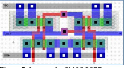
Also, we have compared our QCA designs with conventional CMOS technology. Fig. 7 shows the layout of a RS flip flop implemented with 90 nm CMOS technology. The layout shown in Figure 7 has the approximate area equal to 9.65 µm2. In comparison with this CMOS design, the required areas for our QCA design shown in Fig.3 is about 742 times smaller. Table 2 shows the comparison between the proposed QCA designs and the CMOS work. As shown in Table 2, the proposed QCA RS flip flop in Figure 3 has around 742 times, 174 times, 2750000000 times and 456.8 times improvements in terms of area, delay, power and frequency, respectively.
Figure 7. Layout of a CMOS RSFF.
Table 2. Comparison with CMOS Technology.
Comparison RS flip flop Designs
Fig.7 Fig.3
Approximated
area (µm2) 9.65 0.013
Delay (ps) 122 0.700
Power (μW) 55 8
2 10
Frequency (GHz) 1.25 571
4. CONCLUSION
In this paper, we proposed optimized QCA RS flip flops. The proposed structures are validated using the QCADesigner software. In comparison with the previous works, the results showed that these QCA RS flip flops are better in terms of area, cell count and delay. In comparison with the best previous design the best our design reduced the area and cell count by 67% and 51 %, respectively. Therefore, we can use these structures to design nanoscale circuits.
REFERENCES
1. Walus, K., Wang, W., Julliaen, G.A. (2004). “Quantum Cellular Automata Adders”, IEEE Nanotechnology conf., 3: 461-463.
2. Lent, CS., Tougaw, PD., Porod, W. (1994). “Quantum Cellular Automata: the Physics of Computing With Arrays of Quantum Dot Molecules”, IEEE Computer Society Press, Silver Spring, 5-13.
3. Walus, K. (2003). “Computer Architecture structure for Quantum Cellular Automata”, IEEE Nanotechnology conf. 3: 1435-1439.
4. Walus, K., Schulaf, GA. (2004). “Circuit Design Based on Majority Gates for Application with Quantum Dot Cellular Automata“, IEEE Nanotechnology conf., 4: 1350-135.
5. Momenzadeh, M., Huang, J., Lombardi, F., (2005). “Defect Characterization and Tolerance of QCA Sequential Devices and Circuits“, IEEE International Symposium on Defect and Fault Tolerance in VLSI Systems, 199-207.
7. Dallaki, H., Mehran, M., (2015). “Novel Subtractor Design Based on Quantum-Dot Cellular Automata (QCA) Nanotechnology“, Int. J. Nanosci. Nanotechnol. 11(4): 257-262.
8. Safavi, A., Mosleh, M., (2016). “Presenting a New Efficient QCA Full Adder Based on Suggested MV32 Gate“, Int. J. Nanosci. Nanotechnol. 12(1): 55-69.
9. Kianpour1, M., Sabbaghi-Nadooshan, R., (2014). “Novel Design of n-bit Controllable Inverter by Quantum-dot Cellular Automata“, Int. J. Nanosci. Nanotechnol. 10(2): 117-126.
10.Nath Sasamal, T., Singh, A.K., Mohan, A., (2016). “An optimal design of full adder based on 5-input majority gate in coplanar quantum-dot cellular automata“, Optik-International Journal for Light and Electron Optics. 127(20): 8576-8591.
11.Rao, N.G., Srikanth, P.C., Sharan, P., (2016). “A novel quantum dot cellular automata for 4-bit code converters“, Optik-International Journal for Light and Electron Optics. 127(10): 4246-4249.
12.Heikalabad, S.R., Navin, A.H., Hosseinzadeh, M., (2016). “Content addressable memory cell in quantum-dot cellular automata“, Microelectronic Engineering. 163: 140-150.
13.Mohammadi, M., Mohammadi, M., Gorgin, S., (2016). “An efficient design of full adder in quantum-dot cellular automata (QCA) technology“, Microelectronics Journal. 50: 35-43.
14.http://www.mina.ubc.ca/qcadesigner, (2016).
15.Jagarlamudi, HS., Saha, M., Jagarlamudi, PK., (2011). “Quantum Dot Cellular Automata Based Effective Design of Combinational and Sequential Logical Structures“, World Academy of Science, Engineering and Technology. 60: 671-675.
16.Vetteth, A., Walus, K., Dimitrov, VS., Jullien, GA., (2003). “Quantum-dot Cellular Automata of flip-flops”, The National Conference on Communications (NCC). 368-372.