FPGA Implementation of Programmable Systolic Array
for Sinusoidal Sequence Generation
Noor Kareem Jumaa
Al-Mansour University College Computer Technology Engineering Dept
Baghdad, Iraq
ABSTRACT
Systolic array computation can be done by the arrangement of multi processors in an array which enables the data to follows synchronously across the array and between neighbor processor which speeded up the computation comparing with single processor computation. A sinusoidal sequence is generated in a considerably shorter time by using a fully pipelined systolic array.
FPGA (Field Programmable Gate Array) is selected as a VLSI (Very Large Scale Integration) platform device since, FPGA can provide a certain computations at very high frequencies with systolic computing. The present work is concentrated on developing hardware model for systolic array implementation for sinusoidal sequence generator using VHDL (Very High Speed Integrated Circuits Hardware Description Language) as a platform. The design is implemented using simulator and synthesized on Cyclone III FPGA board.
Keywords
Systolic Array, FPGA, VLSI, VHDL, Altera
1.
INTRODUCTION
Systolic array is a group of processors arranged in an array where data follows across the array synchronously, usually with different data flowing in different directions. At each step, each processor takes in data from one or more neighbors (e.g. North and west), processes it and outputs the result in the next step in the opposite direction (e.g. south and east), Figure (1) shows the two dimensional of processor elements (PE) systolic array structure. [1, 2]
In systolic computing, FPGAs can be used as dedicated computers in order to achieve certain computations at very high frequencies. In recent years, FPGAs have been considerably improved the speed, density, and functionality, which makes them ideal for system-on-a-programmable-chip (SOPC) designs for a wide range of applications. Instead of costly multicore Digital Signal Processing (DSP) systems, designers can promote from high density and high performance FPGAs.[2,3]
In this work, an effective implementing method of a systolic array for truncated sine series is implemented using FPGA.
For efficient implementation and maximum speed-up, minimum logic elements of FPGA Kit was used, i.e. the systolic array of truncated sine series is implemented in an enhanced method using FPGA in order to speed up the processing with using minimum logic elements.
This paper is organized as follows: section 2 presents the description of the design of a systolic array for truncated sine series. In section 3, the implementation purpose is described; in section 4 the FPGA and VHDL implementation of systolic array is described. Section 5 present results and discussion and finally conclusions are presented in section 6.
2.
SYSTOLIC ARRAY FOR
TRUNCATED SINE SERIES
The series for sin x can be shown to be
(1)
The dependence graph for the computation of sin x is shown in Figure (2), the figure illustrate the operations assigned to a vertex of the dependence graph. The number of terms in the truncated series is taken to be three. The parameters used to calculate the truncated sine series used in the programmable systolic array are: x, sum, ai, fi, pi, and ui, initially in the first PE: sum=0, ai= fi= pi=1, and ui=-1. The processing that performed by the PEs are shown in the following equations: x'=x (2)
ao=ai x2 (3)
uo=- ui (4)
sum'=sum+(uo ai x)/fi (5)
po= pi +2 (6)
fo=po (pi +1) fi (7)
Where x', sum', ao, fo, po, uo are the outputs of the PEs. Figure
Fig.1: Two-Dimensional Systolic Array Structure
Fig.2: Operation assigned to a vertex of the PE [3]
x
Sum
a
if
ip
iu
iX'
Sum'
a
of
oP
oFig. 3: systolic array for the computation of sin x. [3]
3.
IMPLEMENTATION PURPOSE
Since VHDL finds many application due to its very high speed integrated circuit. The VHDL program can be loaded into the chip and can be used by tool user. Also this language can be used to define complex electronic systems. [1] And because of the flexible methodologies provided by VHDL, this implementation is done by using VHDL.
The point of this implementation is to resolve a wide scale of computational problems by designing and implementing the systolic array architecture on FPGA.
Properties of this implementation are:
1. Both hardware and software flexibility (i.e. FPGA technology).
2. Parallelism (i.e. systolic array architecture). 3. Scalability in the designed architecture. 4. Fully pipelined architecture.
4.
FPGA AND VHDL
IMPLEMENTATION OF THE
SYSTOLIC SINE ARRAY
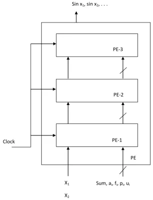
The environment for the programming implementation circuit is based on VHDL. This implementation fully pipelined systolic array to generate sine series is based on Altera Cyclone III DE0 board. The implementation is modeled based on the using of minimum logic elements in order to speed up the processing and provide more flexibility of the design; this is done by design a single PE and divides it into three virtual PE. Each PE is perform its processes pipelining depends on clock event. Figure (4) shows the FPGA implementation model.
PE entity is designed with two ports only: clock port and sum port, in order to decrease the I/o processing, other data (i.e. x, ai, . . . etc) is designs as a signal which allows these data to
follows internally and locally.
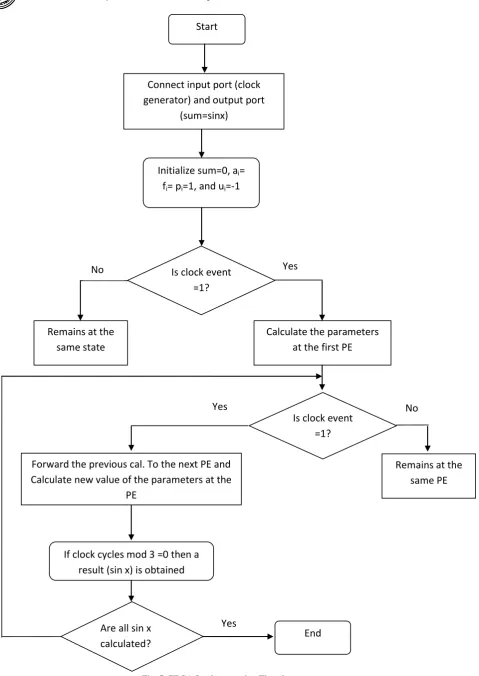
Clock signal is driven from the external FPGA clock quartos with 50 MHZ which provide a clock pulse with 20 nsec. At each clock cycle (i.e. clock event, clock='1'), the sub PEs are perform their calculations and during the next event (i.e. at the beginning of the positive edge) the results of the calculations are forwarded to the next sub PE until the three sub PEs perform their processing and the result (sin x) is obtained from the last sub PE.
Figure (5) shows the flowchart of the implementation and Figure (6) shows the VHDL designed entities.
5.
RESULTS AND DISCUSSIONS
The performance analysis of this implementation can be stated with the following parameters:
1. Each sin x is done after 3 clock cycles, and each clock cycle is 20 nsec thus, each sine series is completed after 60 nsec. All the sine series are obtained after (number of required sine series+ 3 (number of designed PEs) ; thus, if four sine series required to be obtained systolically (i.e. sin x1, sin x2, sin x3, sin x4) then, last sine series (i.e. sin x4) is obtained after 7 nsec which means after 140 nsec. 2. Logic elements used in this implementation are minimized to zero, because the elements used in this design are mathematical operation as described in [3].
3. Just three pins are used: one for the clock, other one for the output x which is equal to the input x (see eq. 2), and the last one is assigned to the output sum which perform the result of sin x.
4. No registers are used since, the data are follow as an internal signal as mentioned in 4, and the clock and the outputs are assigned as I/O FPGA ports. The report of the implementation is shown in Figure (7)which perform the flow FPGA report.
1
1
-1
1
0
X1 X2 X3 . . XnFig. 4: FPGA Implementation Model
X
1X
2.
.
Sum, a
i, f
i, p
i, u
iSin x
1, sin x
2, . . .
Clock
PE
PE-1
PE-3
Fig. 5: FPGA Implementation Flowchart
Remains at the
same state
Calculate the parameters
at the first PE
Is clock event
=1?
Start
Connect input port (clock
generator) and output port
(sum=sinx)
Initialize sum=0, a
i=
f
i= p
i=1, and u
i=-1
Is clock event
=1?
No
Yes
No
Remains at the
same PE
Yes
Forward the previous cal. To the next PE and
Calculate new value of the parameters at the
PE
If clock cycles mod 3 =0 then a
result (sin x) is obtained
Are all sin x
Fig.6: VHDL Designed Entity
Fig.7: FPGA combination report
6.
CONCLUSION
The design of fully pipelined systolic array for the sine series working with frequency of 50 MHZ and the design was
optimized using structural style compared with behavioral style. The designed circuit has been implemented on FPGA and simulated using Quartus II web edition software version
VHDL Clock Entity
9. Again, using Altera DE0 cyclone III board. By implementing such designs in VHDL on easily understands the behavior of designing aspects effectively. If this prototype is implemented in real time then there will be n number of advantages benefited to the mankind.
7.
REFERENCES
[1] Bairu K. Saptalakar, Deepak Kale, Mahesh Rachannavar, and Pavankumar M. K., "Design and Implemetation of VLSI Systolic Array Multiplier for DSP Applications", International Journal of Scientific Engineering and Technology, Vol. 2, ISSN: 2277-1581, India, 2013. VLIS [2] Himani, Harmanbir Singh Sidhu, "Design and Implementation Modified Both Algorithm and Systolic
Multiplier Using FPGA", International Journal of Engineering Research & Technology (IJERT), Vol.2, ISSN: 2278-0181 ,2013.
[3] Rakesh Birle and Lalit Bandil, "Design and FPGA Implementation of Systolic Array Architecture for Matrix Multiplication", International Journal of Engineering and Advanced Technology (IJEAT), Vol. 1, ISSN: 2249-8958, India, 2012. VLIS
![Fig. 3: systolic array for the computation of sin x. [3]](https://thumb-us.123doks.com/thumbv2/123dok_us/1253293.1630726/3.595.58.279.87.504/fig-systolic-array-computation-sin-x.webp)