Analysis of Mid-range Wireless Power Transfer Circuits
Based on Reactance Function and Image Impedance
Yasuyuki Okumura*, Masahiro Yamamoto, Katsuyuki Fujii, Naoki Inagaki
Faculty of Science and Engineering, Nanzan University, Aichi, Japan
Abstract
This paper proposes a novel method to analyze the mid-range wireless power transfer circuits comprised of square coils and capacitors and maximize overall efficiency. The method is based on the equivalent circuit model derived from the reactance function and image impedance. The mid-range circuits are promising as an efficient wireless power transfer method using near field electromagnetic waves. However, no simple design and the analysis methods are available for wireless power transfer. This paper assumes both transmitter and receiver antennas are identical and electrically small. It analyzes the resonance frequencies of the even and odd modes, which are used to model the equivalent circuit describing the actual wireless power transfer circuits. This paper also analyzes the transfer efficiency using the equation of the equivalent circuit, simulation software based on the moment method and an experiment. It clarifies that the analytical values derived by the proposed method and the simulation results mostly agree with the measured values. As a result, the mid-range wireless power transfer circuits designed using the proposed analysis method achieve high efficiency.Keywords
Mid-range power transfer, Reactance function, Image impedance1. Introduction
In recent years, near field connection antennas are being widely used in applications such as radio frequency identifier (RFID) tags [1], body-centric communication [2], and wireless power transfer [3]. Wireless power transfer realizes flexible power charging without wires or plugs, and its application to electric vehicles is deemed essential since such vehicles need frequent charging. If high efficiency wireless power transfer circuits can be developed with large air gaps, electric vehicles could be charged in parking areas.
Conventional wireless power transfer can be realized using three technologies: electromagnetic induction, microwave transfer, and the laser transfer. Only the electromagnetic induction is widely and commercially used but in limited environments where the transfer distance is less than 1cm. However, mid-range power transfer over 10cm or so has been proposed with the use of 20 to 40 kHz signals. In addition, mid-range power transfer of around 2m has been proposed through the use of electromagnetic resonance. As its theoretical efficiency is around 45 to 50% with a 2m air gap, and over 90% at under 1m, it is a promising technology [3-5]. Unfortunately, the current
* Corresponding author:
[email protected] (Yasuyuki Okumura) Published online at http://journal.sapub.org/eee
Copyright © 2017 Scientific & Academic Publishing. All Rights Reserved
analysis approach, which uses mode coupling theory and a Q factor that describes the energy conservation of the circuit, makes it difficult to design more efficient circuits [6-10]. A simpler analysis theory of mid-range power transfer is needed to design circuits with less difficulty.
2. Analysis Model of Mid-Range Power
Transfer Circuit Based on the
Impedance Matrix
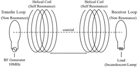
The mid-range power transfer circuits consist of two pairs of an excitation coil and a resonance coil, one pair for the transmitter and the other for the receiver, as shown in Figure 1. This paper assumes that both pairs are identical, i.e. the excitation and resonance coils have the same shape and size. The RF generator powers the excitation coil in the transmitter, and the load receives the power through the excitation coil in the receiver. This configuration was proposed in [3, 4], where the RF frequency is of the order of MHz; the resonance coil maximizes the transmission distance and efficiency. In the configuration, the resonance coil is helically shaped, and its resonance frequency equals that of the RF generator.
Figure 1. Mid-range power transfer circuit configuration [3]
2.1. Efficiency of the Power Transfer Circuit [11]
The general equivalent circuit for the input and output circuit (the power transfer circuit) is shown in Figure 2, where the coils and the transmission space between them characterize a 4-port circuit with impedance matrix Z. This paper assumes the 4-port circuit is linear, reciprocal and passive, which characterizes the reflectors, the scatterers and the absorbers of the radio signals. Given that the RF generator and load are connected to port1 and port2, respectively, the efficiency of the power transmission between the generator and the load is described as |S12|2=|S21|2,
where S12 and S21 are elements of the scattering matrix
[12-13]. The design objective for the power transfer circuit is determining impedance Z1 of the RF generator and
impedance Z2 of the load so as to maximize |S12|2=|S21|2. Each
impedance is described as a combination of resistance and reactance, i.e. Z1=R1+jX1 and Z2=R2+jX2.
Given the above notation, efficiency is described as follows [9];
(
)(
)
2
2 2 21 1 2
12 21 2
1 11 2 22 12 21
4
,
= =
+ + −
z R R
S S
Z z Z z z z (1)
where zij (i = 1 or 2, j = 1 or 2) is the element of Z.
Efficiency |S12|2 is maximized by impedance matching based
on the theory of conjugate image impedance [11]. Provided the load contains only the resistance component, the
conjugate image impedance is equal to the image impedance. Given z11=r11+jx11 etc., the theory gives the image impedance
for transmitter side Zt and that for the receiver side Zr as
follows;
(
)
11 θ θ 11,
= + −
t r x
Z r j jx (2)
(
)
22 θ θ 22,
= + −
r r x
Z r j jx (3) where
2 2
12 12
11 12 11 12
1 1 ,
θ = − +
r r rr r rx (4) 12 22
11 22 ,
θx =r x
r r (5)
The maximum efficiency is achieved when impedance Z1
of the RF generator is equal to Zt, while impedance Z2 of the
load is equal to Zr [11].
Figure 2. One input and one output circuit
2.2. Analysis of the Impedance Matrix
To analyze the efficiency, |S12|2, all elements of Z must be
assessed in the mid-range power transfer circuit, as shown by eq.(1). The circuit model shown in Figure 3(a) is a 2-port circuit and thus linear, reciprocal and passive. In this model, the inductance of the excitation coil and the resonance coil are denoted as L1 and L2, respectively. Regarding the
resonance coil, capacitor C is inserted for impedance matching. Mutual inductances M12, M13, M14,and M34, and
resistances R1’ and R2’ representing the loss, are also
considered for the circuit analysis as shown in the figure. To derive Z of the circuit, the model should be modified to a 4-port circuit, as shown in Figure 3(b). If ports 3 and 4 are shunted, see Figure 3(b), it becomes identical to the circuit of Figure 3(a). First of all, impedance matrix Z4port of the 4-port
circuit can be described using the angular frequency ω=2πf
as follows;
11 12 13 14 11 12 13 14 21 22 23 24 12 11 14 13 4
31 32 33 34 13 14 33 34 41 42 43 44 14 13 34 33 '
1 1 12 13 14
'
12 1 1
ω ω ω ω
ω ω ω
′ ′ ′ ′ ′ ′ ′ ′
′ ′ ′ ′ ′ ′ ′ ′
= =
′ ′ ′ ′ ′ ′ ′ ′ ′ ′ ′ ′ ′ ′ ′ ′
+
+ =
Z port
z z z z z z z z
z z z z z z z z
z z z z z z z z
z z z z z z z z
R j L j M j M j M
j M R j L j M14 13
'
13 14 2 2 34
'
14 13 34 2 2
1 .
1
ω
ω ω ω ω
ω
ω ω ω ω
ω
+ +
+ +
j M
j M j M R j L j M
j C
j M j M j M R j L
j C
Using elements z’ij of Z4port, the impedance matrix Z of the
two-port circuit shown in Figure 3(a) is given as follows;
(
)
(
)
(
)
(
)
11 12
21 22
2 2
13 14 33 13 14 34
11 2 2
33 34
2 2
13 14 34 13 14 33
12 2 2
33 34
2 2
13 14 34 13 14 33
12 2 2
33 34
2 2
13 14 33 13 1
11
2
2
2
2
=
′ + ′ ′ − ′ ′ ′
′ −
′ − ′
=
− ′ + ′ ′ + ′ ′ ′
′ −
′ − ′
′ ′ ′ ′ ′ ′
− + +
′ −
′ − ′ ′ + ′ ′ − ′ ′ ′ −
Z
z z
z z
z z z z z z
z
z z
z z z z z z
z
z z
z z z z z z
z
z z
z z z z z
z 2 2 4 34
33 34
,
′
′ − ′
z
z z
(7)
where its derivation process is described in the Appendix. By determining the RLC values and substituting the elements zij
of eq.(7) into eq.(1), efficiency |S12|2 can be calculated.
(a) Two-port circuit model (b) Four-port circuit model
Figure 3. Analysis model of mid-range power transfer circuit
3. Analysis Based on the Equivalent
Circuit
Figure 4. Equivalent circuit model
This section describes the other analysis based on the equivalent circuit. The equivalent circuit of the mid-range power transfer circuit can be elucidated using the even and the odd mode resonance frequencies, where the loss caused by the copper of the circuit is negligible [12]. The equivalent
circuit used in this analysis is shown in Figure 4, where identification means determining the values of L and C in Figure 4, given the values of L1, L2, C, M12, M13, M14 and M34
in Figure 3(a).
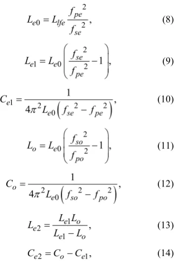
3.1. Determination of the Values of Inductance and Capacitance [14-15]
Using the resonant and the anti-resonant frequencies, the L and C values of Figure 4 can be described as follows;
2
0= pe2 ,
e lfe
se f
L L
f (8) 2
1 0 2 1 ,
= −
se
e e
pe f
L L
f (9)
(
)
1 2 2 2
0
1 ,
4π
=
− e
e se pe
C
L f f (10) 2
0 2 1 ,
= −
so
o e
po f
L L
f (11)
(
)
2 2 2
0
1 ,
4π
=
− o
e so po
C
L f f (12) 1
2
1 ,
= − e o e
e o
L L L
L L (13)
2= − 1,
e o e
C C C (14) where fse and fpe are the resonant frequency and the
anti-resonant frequency of the even mode, and fso and fso are
those of the odd mode, respectively. The value of Llfe is the
inductance of the even mode in the low frequency range. The analysis method of these frequencies is proposed in Section 3.2 and 3.3. The value of Llfe depends on the shape and the
size of the coil, and is derived by numerical analysis as described in Section 4.
Once the equivalent circuit shown in Figure 4 is identified, all elements of the scattering matrix can be derived as follows; impedance matrix Z can be derived from the equivalent circuit as a ladder circuit, which is converted into transfer matrix F and to scattering matrix S. In S, element S21
means the transfer efficiency.
3.2. Analysis of Resonant and Anti-Resonant Impedances
The resonant and the anti-resonant frequencies of the even and the odd modes can be derived by analyzing the impedance of the mid-range power transfer circuit model, which will be described in Section 3.3. To analyze the impedance, the model is modified into a 4-port circuit, as described in Section 2. By inserting R1’=R2’=0 into eq. (6),
impedance matrix Z4port of the 4-port circuit can be written as
11 12 13 14
21 22 23 24
4
31 32 33 34
41 42 43 44
1 12 13 14
12 1 14 13
13 14 2 34
14 13 34 2
1 , 1 ω ω ω ω ω ω ω ω ω ω ω ω ω ω ω ω ω ω = + = + Z port
z z z z
z z z z
z z z z
z z z z
j L j M j M j M
j M j L j M j M
j M j M j L j M
j C
j M j M j M j L
j C
(15)
11 12 13 14
1 1
21 22 23 24
2 2
31 32 33 34
3 3
41 42 43 44
4 4 . =
z z z z
V I
z z z z
V I
z z z z
V I
z z z z
V I
(16)
In the above equation, the current of port i is denoted by Ii
(i=1,2,3,4), and the voltage of this port is denoted by Vi.
Provided V3=V4=0, eq. (16) describes the mid-range power
transfer circuit shown in Figure 3(a).
Even mode impedance Ze is calculated by deriving input
current Ie1 into port 1, provided the same voltage, E, is given
to ports 1 and 2, which is the condition of even mode operation. On the other hand, regarding odd mode impedance Zo, input current Io1 must be derived when
voltages E and –E are given to port 1 and port 2, respectively. Based on the above definition, the even and the odd mode impedances are written as follows;
1, = e e E Z
I (17)
1. = o o E Z
I (18)
In the even mode, the conditions I1=I2 and I3=I4 are applied
to eq. (16). By eq. (15), z11=z22, z33=z44, and zmn=znm(m≠n),
which lead to the following;
11 12 13 14 1
13 14 33 34 3 ,
0 + + = + + e e
z z z z I
E
z z z z I (19)
(
)
(
) (
)
(
)
2
11 12 33 34 13 14
33 34 2 13 14 1 12 2 34 . 1 ω ω ω ω ω + + − + = + + = + − − +
e z z z z z z
Z
z z
M M
j L M
L M
C
(20)
In the odd mode, by applying the conditions of I1=-I2
and I3=-I4 to eq. (16), voltage E, current Ioi (i=1 or 3) and
impedance Zo are written as follows;
11 12 13 14 1
13 14 33 34 3 ,
0 − − = − − o o
z z z z I
E
z z z z I (21)
(
)
(
) (
)
(
)
2
11 12 33 34 13 14
33 34 2 13 14 1 12 2 34 . 1 ω ω ω ω ω − − − − = − − = − − − −
o z z z z z z
Z
z z
M M
j L M
L M
C
(22)
Based on the above calculation, image impedance Zi can
be derived as follows;
(
)
(
)
2 13 14 1 12 2 34 2 13 14 1 12 2 34 1 . 1 ω ω ω ω ω ω ω ω ω = − = − − − − − + × + − − + i e o
Z Z Z
M M L M L M C M M L M L M C (23)
3.3. Analysis of Resonant and Anti-Resonant Frequencies
The resonant frequency is defined as the frequency that yields zero reactance, and the anti-resonant frequency makes the reactance infinite. Therefore, from setting the condition
Ze=0 and Ze=∞ in equation (20), fse and fpe are derived as
follows;
(
)
213 14 2 34 1 12 1 , 2π = + + − + se f M M
C L M L M (24)
(
2 34)
1 . 2π = + pe f
C L M (25)
On the other hand, seting Zo=0 and Zo=∞ in equation (22), fso and fpo are derived as follows;
(
)
213 14 2 34 1 12 1 , 2π = − − − − so f M M
C L M
L M (26)
(
2 34)
1 . 2π = − po f
C L M (27)
Using these results, the values of L and C in the equivalent circuit shown in Figure 4 can be derived from equations (8) to (14). Provided fse=fpo, impedance matching is available for
any frequency f satisfying the condition; fpe < f < fso [15].
4. Physical Implementation of the
Mid-Range Power Transfer Circuit
band, which is a standard and commercially used band. The ISM band includes frequencies such as 130 to 135 kHz, 13.56 MHz, 433 MHz, 900 MHz, and 2.45 GHz. One example of 13.56 MHz signal use is RFID, which is a touch-less integrated circuit (IC) that transfers information and electric energy. Since the wavelength of 13.56 MHz frequency radio is 22.12 meters and its radiansphere is 3.52 meters, the antenna should be smaller than a ball with radius equal to the radiansphere. In the MHz frequency range with longer wavelength, the antenna size becomes larger than the above, which causes difficulties in the practical use. Although this paper focuses on the 13.56MHz considering the condition, the analysis methods proposed in the paper can be applied to this frequency band. In addition, this paper assumes the characteristic impedance is 50 ohm, a common commercial setting. The physical structure of the antennas is shown in Figure 5, where each coil is a single square turn of copper sheet. The transmitter and the receiver consist of two coils, where the inner coil transmits or receives the power, and the outer one is the resonant coil. In the transmitter and the receiver, both the inner and the outer coils lie on the same hypothetical plane and the center of each coil lie on the same hypothetical line. Each coil is made up of copper sheet, 1 millimeter thick and 25 millimeter wide, and a ceramic capacitor. The copper sheet easy to process and is suitable for antenna implementation. The ceramic capacitors offer a flat reactance characteristic in the high frequency range, and are small.
Figure 5. Physical implementation of power transfer circuit
4.1. Analysis of the Inductance and Capacitance of the Antenna
The square outer coil has length of a meters, and that of the inner coil is b meters, where both coils are parallel to the
x-y plane. The distance between the transmitting coil and the receiving coil is taken to be s millimeters. In the transmitter, the excitation coil is loaded with the voltage source and a resistor (R=50Ω), and the resonance coil is loaded with a capacitor (C Farad). The load of the receiving coil is a
resistor (R=50Ω), and the load of the resonance coil is a capacitor equal to that in the transmitter.
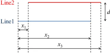
Figure 6. Analysis model of mutual inductance of two lines
The self-inductance and mutual inductance can be derived from Neumann’s formula. Since any pair of sides are parallel or orthogonal with each other in the square shaped coil, the inductance is determined only by the parallel pair according Neunann’s formula. Therefore, as a first step, the mutual inductance M between the two parallel lines shown in Figure 6 is calculated as follows;
(
)
(
)
(
)
(
)
2 2 2 2
2 2 2 2
2 2 2 2
1 1 1 1
2 2 2 2
3 3 3 3
2 2 2 2
2 2 2 2
log 4
log
log
log ,
µ π
= + + − + +
− + − − + +
− + − − + +
+ + + − + +
M x d x x x d
a d a a a d
x d x x x d
a d a a a d
(28)
where d=y2-y1, a1=x2-x1, a2=x3-x1, and x1, x2, x3, y1 and y2 are
coordinates of the end points of the two parallel lines. Regarding the square coil, only the parallel lines contribute to the inductance, since the inductance is, according to Neumann’s formula, expressed as the inner product of the vectors along the two lines comprising the coil. Therefore, mutual-inductances M12, M13, M14, M34 and self-inductances L1 and L2 can be derived from equation (28).
Provided the outer coil is configured as a copper line with radius r meters, self-inductance L is
(
)
2 2
2 2
1 2
2µ 2 log .
π
+
= − − + + +
+ +
r
L a r a a r a
a a r (29)
Mutual inductance M of the two outer coils (one side is a
meters in length) is written as follows;
(
)
2 2 2 2
2 2 2 2
2 2
2 2 2 log ,
2
µ π
+ + +
= − + + + +
+ +
a s a a s
M s a s a s a
s a a s
(30)
2 1 ,
ω
=
C
L (31)
where ω is the resonance angular frequency.
4.2. Designing the Antenna
Figure 7. Analysis results of resonance frequencies
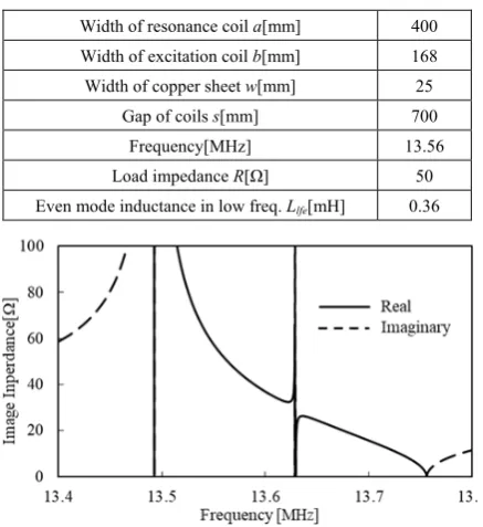
Table 1. Design parameters of power transfer circuit Width of resonance coil a[mm] 400 Width of excitation coil b[mm] 168 Width of copper sheet w[mm] 25
Gap of coils s[mm] 700
Frequency[MHz] 13.56
Loadimpedance R[Ω] 50
Even mode inductance in low freq. Llfe[mH] 0.36
Figure 8. Analysis results of Image impedance
The design parameters of the antennas for mid-range power transfer are variables such as; width w of the copper sheet, side length of the square resonance coil a, side length of the square excitation coil b, and the gap between the transmitter and the receiver coils s. As initial conditions, this paper assumes that w, a and s are 25mm, 400mm, and 700mm, respectively, and the operation frequency
f is 13.56MHz. By using equations (29) and (30), self-inductance L and mutual inductance M can be calculated, and used in eqs. (24) to (27) to calculate resonance frequencies fpe, fse, fpo, and fso, respectively. The relation
between b and the four resonance frequencies is shown in Figure 7. Applying the condition fse=fpo described in Section
3, side length of the square excitation coil b is 168mm. All
parameters of the designed antennas are summarized in Table 1. Using eq. (23), the relation between frequency and image impedance Zi is described in Figure 8, where the
image impedance is real in the 13.49 to 13.75MHz range, and becomes 50ohm at 13.56MHz.
5. Model for Simulation and Experiment
This section outlines the simulation model and the experimental setup.
5.1. Simulation Model
The electromagnetic field analysis software FEKO [16] was used to analyze the power transfer efficiency by simulation. FEKO offers a numerical method for computational electromagnetics in a wide range of electromagnetic problems. The simulation model reproduces the transmitter and the receiver antennas shown in Figure 5. Antenna material is copper with conductivity of 57.6x10⁶
S/m, and relative permeability of 0.999991.
The simulation is carried out not only to determine the power transfer efficiency, but also identify the equivalent circuit parameters described in Section 4. The inductance and the capacitance values of the equivalent circuit, Le0, Le1, Le2, Ce1, and Ce2, are summarized in Table 2 based on the
simulation.
Table 2. Identification results of equivalent circuit Inductance Le0[mH] 0.352
Inductance Le1[mH] 7.610
Inductance Le2[mH] 88.42
Capacitance Ce1[nF] 18.29
Capacitance Ce2[nF] 1.154 5.2. Experimental Setup
The experimental setup is shown in Figure 9, where the square antennas are mounted on wooden frames. The power transfer efficiency between the transmitter and the receiver antennas was measured using an Agilent E5071C network analyzer.
6. Model for Simulation and Experiment
This section describes the results of transfer efficiency
S21 together with reflection coefficient S11 derived by the
analysis based on the impedance matrix in Section 2, the analysis using the equivalent circuit in Section 3, the simulation, and the experiment. The results related to frequency are shown in Figure 10. Regarding the accuracy of the above values, the significant figures of the analysis and the simulation are four digits. The trace noise of the network analyzer is 0.003dBrms in the experiment. The results derived by the analysis, simulation, and experiments show almost the same characteristics; that this, the two analysis methods introduced in this paper agree with the experiment and simulation results.
Maximum efficiency (S21) is -0.0064dB at 13.56MHz by
the analysis of the impedance matrix (Section 2), -0.00071dB at 13.56MHz by the analysis of the equivalent circuit (Section 3), -0.87dB at 13.56MHz by the simulation, and -1.54dB at 13.56MHz measured in the experiment. The measured value of S21 is smaller than the analysis and
simulation equivalents due to the copper loss. The mid-range wireless power transfer circuits designed using the proposed analysis method achieved high efficiency. To increase the efficiency, low-loss material such as Litz Wire could be used for the antenna coil.
Figure 10. S-parameter characteristics
7. Conclusions
This paper proposed a novel method for analyzing the mid-range wireless power transfer circuits comprised of a square coil and capacitor and maximizing overall efficiency. The method is based on the equivalent circuit model derived from the reactance function and image impedance. This paper assumes that transmitter and receiver antennas are identical and electrically small. It analyzed the resonance frequencies of the even and odd modes, and used them to model the equivalent circuit of the actual wireless power transfer circuits. This paper also analyzed the transfer efficiency using the equation of the equivalent circuit, simulation software based on the moment method and an experiment. It clarified that the analytical values derived by the proposed method and the simulation results mostly agree
with the measured values. As a result, the designed mid-range wireless power transfer circuits achieved high efficiency.
ACKNOWLEDGEMENTS
This work was supported by the Nanzan University Pache Research Subsidy I-A-2 for the 2017 Academic year.
Appendix
Provided ports 3 and 4 are shunted, see Figure 3(b), the circuit becomes identical to that of Figure 3(a). In this case, the voltage and the current of each port are given as follows;
11 12 13 14 1
1
12 11 14 13 2
2
13 14 33 34 3
14 13 34 33 4
. 0
0
′ ′ ′ ′
′ ′ ′ ′
= ′ ′ ′ ′
′ ′ ′ ′
z z z z I
V
z z z z I
V
z z z z I
z z z z I
(A1)
In the two-port circuit, the voltage and the current of each port are given as follows;
[ ] [ ] [ ] [ ]
{
1}
1 1
11 12 22 21
2 2 ,
−
= −
V I
Z Z Z Z
V I (A2)
where
[ ]
[ ]
[ ]
[ ]
13 14
11 12
11 12 21
14 13
12 11
33 34
22
34 33
, ,
.
′ ′
′ ′
= = =
′ ′
′ ′
′ ′
= ′ ′
z z
z z
Z Z Z
z z
z z
z z
Z
z z
(A3)
Eq.(7) is derived by inserting (A3) into (A2).
REFERENCES
[1] K. Uesaka and M. Takahashi, “Antennas for Contact-Less IC Card/RFID Tag Systems,” IEICE Trans. Communications, vol. J89-B, no. 9, pp. 1548-1557, 2006.
[2] P. S. Hall and Y. Hao, Antennas and Propagation for Body-centric Wireless Communications, Artech House, 2006.
[3] A. Kurs, A. Karalis, R. Moffatt, J. D. Joannopoulos, P. Fisher, and M. Soljacic, “Wireless power transfer via strongly coupled magnetic resonances,” Science, vol.317, no.5834, pp.83-86, 2007.
[4] A. Karalis, J. D. Joannopoulos, and M. Soljacic, “Efficient wireless non-radiative mid-range energy transfer,” Annals of Phisics, 323, pp.34-48, 2008.
[6] T. Ohira, “Maximum available efficiency formulation based on a black-box model of linear two-port systems,” IEICE Electronics Express, vol. 11, no.13, pp. 1-6, 2014.
[7] Q. T. Duong, M. Okada, “Maximum efficiency formulation for inductive power transfer with multiple receivers,” IEICE Electronics Express, vol.13, no.22, pp.1-10, 2016.
[8] B. Minnaert, N. Stevens, “Single variable expressions for the efficiency of a reciprocal power transfer system,” International Journal of Circuit Theory and Applications, online 2016.
[9] Q.T. Duong, M. Okada, “kQ-product formula for multiple-transmitter inductive power transfer system,” IEICE Electronics Express, vol.14, no.3, pp.1-8, 2017.
[10] M. Tamura, Y. Watanabe, I. Takano, “Waveguide-mode wireless power transfer in shielded space with aperture plane,” IEICE Electronics Express, vol.14, no.8, pp.1-8, 2017.
[11] S. Roberts, “Conjugate-image impedances,” Proc. I. R. E. and Waves and Electronics, vol.34, pp.198-204, 1946.
[12] D. Pozer, Microwave Engineering, Fourth Edition, Wiley 2013.
[13] G. Vendelin, A.M. Pavio, and U. L. Rohde, Microwave Circuit Design Using Linear and Nonlinear Techniques, Wiley 1995.
[14] N. Inagaki, S. Hori, “Fundamentals of wireless connections with near field coupled antennas,” IEICE Trans. Communications, vol. J94-B, no. 3, pp. 436-443, 2011. [15] N. Inagaki, S. Hori, “Characterization of wireless connection