EXPERIMENTAL STUDY OF COEFFICIENT OF THERMAL
EXPANSION OF ALIGNED GRAPHITE THERMAL INTERFACE
MATERIALS
Hsiu-Hung Chen
a, Yuan Zhao
b, Chung-Lung Chen
a,*a
Department of Mechanical and Aerospace Engineering, University of Missouri, Columbia, MO 65211 b Teledyne Scientific, Thousand Oaks, CA 91360
A
BSTRACTCarbon-based materials draw more and more attention from both academia and industry: its allotropes, including graphene nanoplatlets, graphite nanoplatlets and carbon nanotubes, can readily enhance thermal conductivity of thermal interface products when served as fillers. Structural-optimization in micro/nano-scale has been investigated and expected to finely tune the coefficient of thermal expansion (CTE) of thermal interface materials (TIMs). The capability of adjusting CTE of materials greatly benefits the design of interface materials as CTE mismatch between materials may result in serious fatigue at the interface region that goes through thermal cycles. Recently, a novel nano-thermal-interface material has been developed, which is composed of tin (Sn) solder and graphite nanoplatlets. CTE of such sort of TIMs can be adjusted to match well with the substrate materials. A customized, optical CTE measuring system was built to measure CTEs of these thin and flexible samples. The averaged CTEs of samples made by this new approach range from -0.267×10⁻⁶/°C to 5×10⁻⁶/°C between 25°C and 137°C, which matches CTEs of typical
semiconductor materials (the CTE of silicon is ~3×10⁻⁶/°C in the same temperature range). This unique CTE-matching feature of a bonding material will have great potential to impact future development of high power microelectronics devices.
Keywords: Graphene, Graphite, Thermal Interface, Thermal Expansion.
* Corresponding author. Email:[email protected]
1. INTRODUCTION
Thermal interface material (TIM) plays a critical role in microelectronics packaging. The main function of a TIM is to thermally connect various components in a microelectronics package. Thermal resistance and the ability to safely bond layers with vastly different coefficient of thermal expansion (CTE) are among the key factors for any TIMs in determining the overall performance and reliability of electronic devices in practical applications. As power density of microelectronics devices increase rapidly, the reliability and instability in the performance of TIMs is a growing concern in many applications (Prasher, 2006).
Conventional TIMs are mostly based on low electrically conductive materials (also low in thermal conductivity), e.g. polymers, greases, or adhesives, mixed with high thermal conductive particles, such as silver, silicon oxide or aluminum oxide. Such sort of TIMs (with K in the range of 0.1 to 4 W/m-°C) is a bottleneck in the whole thermal conductive path and highly restricts heat dissipation from the heat source. Recently, the outstanding thermal properties of carbon nanotubes (CNTs) that can reach up to 3,000 W/m-°C (Balandin et al., 2008) draw extreme attention from both industry and academia. Single wall CNTs (SWCNTs) or multi-wall CNTs (MWCNTs) have been investigated and added to polymer resin materials as fillers (Choi et al., 2001; Biercuk et al., 2002; Yu et al., 2006; Amama et al., 2006; Tao Tong et al., 2007). The enhancement on overall thermal conductivity of such TIMs is obvious; however, it is not as high as was expected. On the other hand, graphene and graphite nanoplatelets (GNPs), prepared from exfoliated natural graphite, provide excellent thermal conductivity on their own and in TIMs matrix (Balandin et al., 2008). Impressively,
the hybrid filler of GNPs and SWCNTs demonstrate a further enhancement of thermal conductivity and surpasses the performance of the individual SWCNT and GNP fillers, due to synergistic effect (Yu et al., 2008). With the same loading ratio, TIM with GNPs fillers outperforms that with SWCNTs fillers by almost double the overall thermal conductivity. GNPs connected by SWCNTs in network qualitatively explain how synergetic effect happens. On the other hand, the introduction of SWCNTs into GNP fillers depresses the electrical conductivity. Such kind of trend actually favors the application of TIMs.
When filled in polymer matrix, GNPs demonstrates remarkable enhancement in thermal conductivity, even better than the case with SWCNTs. This phenomenon has been observed and studied, and is due to weak thermal couple at CNTs/base material interface and prohibitive cost (Shahil and Balandin, 2012). The decrease of K in higher temperatures at higher loading can be described by Umklapp process, where phonon scattering tends to happen more at in higher temperatures (Balandin, 2011).
Instead of introducing pristine carbon materials to polymer composite, chemically functionalized and exfoliated GNPs facilitate nanocomposites by enhancing the interaction between the epoxy and graphite filler. Both thermal conductivity and electrical resistivity have been improved (Ganguli et al., 2008). The use of functionalized GNPs increases K by minimizing interfacial phonon scattering. The addition of GNPs as fillers also delays curing temperature of silicone polymer, because GNPs hinder the mobility of the polymer chains (Raza et al., 2010).
Literature survey also indicates that the CTE of a bonding agent can be changed by infutrating it with fillers of different CTEs. Since
Frontiers in Heat and Mass Transfer
exfoliated graphite has a lower CTE value than the pure polymer, the mixing of graphite and polymer will result in a compromise between the two materials. Wang et al. verified this assumption by their experiments of epoxy mixed with carbon nano-materials (Wang et al., 2009). In their study, obvious CTE reductions were observed on the epoxies when 1% SWCNT and 5% GO were added to them.
It can be noticed that (a) polymer resin, even though it can be enhanced in folds when expensive CNTs or graphene are added, performs relatively poor in thermal conductivity; (b) metal, silicon and carbon (including allotropes) all have high thermal conductivity. Silicon and carbon have small CTEs: some allotropes of carbon even have negative values. Therefore, the effect of CTE mismatch that may cause cracks and fatigues should be taken into consideration when new TIMs are designed. Among the carbon-based materials, graphite seems to be a more promising TIM candidate when both its natural property of thermal conductivity, simplicity and low-cost of fabrication are taken into account.
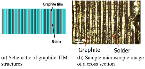
Zhao, el al. (Zhao et al., 2012; Zhao et al., 2011) prototyped a new TIM structure: vertically-aligned graphite laminated with solder layers (Fig. 1). With the laminated structure it is easy to form perfectly straight and highly conductive paths along the desired heat flow direction. The flexibility of the TIM could also be altered by adjusting the thicknesses of the solder layers and graphite sheets so that it could conform to surfaces with different roughness and hardness. They achieved an overall thermal resistivity of approximately 0.035°C/(W/cm2) at an assembly pressure of 30 Psi with a 200-μm-thick TIM (graphite-to-solder ratio of 8), and the number decreased when the compression pressure increased. Achieving the outstanding thermal performance at a much larger bonding line thickness is an attractive and desirable characteristic in microelectronics packaging because thermal induced stress (mainly from the CTE mismatch among materials) is much smaller based on material mechanics principles.
Fig. 1 Schematic and microscopic image of laminated TIM structure.
Applying thermally mismatched materials may result in serious induced stress, or even fatigue/cracks, at the interface region that go through thermal cycles. Therefore, obtaining CTE information for TIM of interests is necessary. There are various dilatometers available to study CTEs for solids (Boccaccini and Hamann, 1999; Neumeier et al., 2008; Winkler et al., 1993). The most commonly used technique is a contact-based expansion measurement during heating (Neumeier et al., 2008; Winkler et al., 1993): when the sample expands, a rod (or a plate) that rests slightly on the surface of the specimen is pushed and the expansion is then measured. This type of measurement requires that the sample is in the direct contact to the sensor, which may disturb the testing results when the sample is fragile or flexible. An optical dilatometer, on the other hand, is a non-contact device that is able to measure CTE of almost any kind of materials (Boccaccini and Hamann, 1999; Raether et al., 2001).
In this research, an experimental study of CTEs of the vertically-aligned graphite/solder TIMs is presented. A series of tests were conducted to quantify impacts of adding metal layers with different thickness onto surfaces of a graphite thin film, on its CTE. A direct optical CTE measurement system was designed and built to execute the
2. EXPERIMENTAL TEST SYSTEM AND APPROACH
2.1 CTE Measurement System
The CTE measurement system is based on an optical approach (Fig. 1), comprised of a microscope (Olympus BXFM, Tokyo, Japan), a CCD camera (UI-1240LE, IDS GmbH, Obersulm, Germany), a motorized XY stage with motorized actuators (8302 Picomotor, Newport Corporation), and a ceramic heater (Ultramic CER-1-01-00005, Watlow, Fenton, MO). Two metal tracks are first screwed onto the stage, which is customized for this test bed. The XY stage is fastened to one track, as shown in II of Fig. 1. Quartz slides sandwich the ceramic heater and a spacer, in order to form a sample holding site. The use of quartz minimizes the heating effect introduced from itself (CTE of 0.33×10⁻⁶/°C) and allows visible light to pass through. A Teflon mounting gadget (with a viewing window) which can be utilized to fasten the sample holding site is fabricated, and allows expansion room for the ceramic heater.
Fig. 2 Optical CTE test bed. From I to VIII: step-by-step assembly procedures.
The sample length along the measuring direction is taken by a caliper, shown in V. Then the sample, able to expand freely, is inserted into the sample holding site. A triangular metal block, serving as a stationary reference, is fastened on the other track (shown in I of Fig. 2). About one tenth of the sample will be extruded out (VI of fig. 2). By doing this, every time before the image is taken at its corresponding set temperature the sample can be “zeroed” by moving the motorized XY stage with an appropriate distance towards the stationary. Temperature is controlled by a DC power supply, providing electric power to the ceramic heater. The sample temperature is monitored by a K-type thermocouple, connected to a data acquisition (DAQ) system (NI-cDAQmx, National Instrument).
When a thin, long sample is heated, its total length usually increases. If the total length is recorded along with its corresponding set temperature, the CTE of a material can then be determined. This change (a) Schematic of graphite TIM
structures
(1)
where α is the CTE, L is the total length of the sample at a reference temperature, ΔL is the difference of sample length before and after heating, and ΔT is the corresponding temperature difference.
2.2 TIM Sample Preparation
TIM samples are made out of graphite films and silver-tin solders (Indalloy 121: Ag 3.5% and Sn 96.5% with CTE: 30×10-6/°C and reflow temperature of 221°C). The graphite film was processed from commercially available graphite sheets (GrafTech International) through a series of heat and compress procedures. Tin metallization was completed by electroplating technique. The detail fabrication processes were discussed in the previous publication (Zhao et al., 2012; Zhao et al., 2011). Our target temperature range is focused between 25°C and lower than 200°C.
3. TEST RESULTS AND ANALYSIS
3.1 Test Bed Validation with Silicon and Copper
Before testing TIM samples, we calibrated our test bed by measuring the CTEs of pure Silicon strip and Copper Alloy 101 (purity of 99.99%), and compared them with literature values. A Silicon strip (24.39mm × 1.2mm × 0.5mm) was tested and its linear expansion during heating is demonstrated in Fig. 3. The measurement was repeated twice on the same sample. A linear curve fit was applied on each data set.
Fig. 3 Linear expansion measurement of a Silicon strip.
By using Eq. (1), α can be determined for each individual measurement between every temperature intervals. The corresponding results for each individual test, curve-fitted with least square method, are listed in Table 1. The measured CTE at 81°C can be treated as an averaged CTE since that temperature is at the middle of our temperature range. The measured CTEs and literature value are shown side-by-side in Fig. 4.
Table 1 Least square fit for each linear expansion measurements on Silicon strip.
Least Square Fit CTE (/°C) Bias
exp 1 y1=0.000078x + 24.388 (R²=0.98) 3.20×10⁻⁶ 5.3%
exp 2 y2=0.000080x + 24.388 (R²=0.99) 3.28×10⁻⁶ 7.9%
exp 3 y3=0.000077x + 24.388 (R²=0.99) 3.16×10⁻⁶ 3.9%
Fig. 4 CTE translated from linear expansion measurements and literature value (Roberts, 1981; Okada and Tokumaru, 1984).
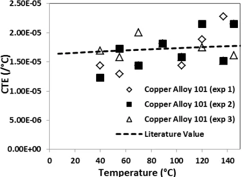
A Copper Alloy 101 (23.33mm × 1mm × 0.25mm) strip was tested and its linear expansion during heating is displayed in Fig. 5. The measurement was repeated twice on the same sample. A linear curve-fit was applied on each data set.
Fig. 5 Linear expansion measurement of a Copper Alloy 101 strip.
Similarly, by dividing the coefficient representing the slope for each first-order line with 23.33mm (original length), the averaged CTEs are obtained and listed in Table 2. The measured CTE at 81°C can be treated as an averaged CTE. The biggest bias among these measurements is 5% larger than the literature value (17.1×10⁻⁶ at 81°C), shown in Fig. 6 (Hahn, 1970).
Table 2 Least square fit for each linear expansion measurements on Copper Alloy 101.
Least Square Fit CTE (/°C) Bias
exp 1 y1=0.00041x + 23.318 (R²=0.99) 17.70×10⁻⁶ 3.5%
exp 2 y1=0.00041x + 23.318 (R²=0.99) 17.79×10⁻⁶ 4%
Fig. 6 CTE translated from linear expansion measurements and literature value (Hahn, 1970).
3.2 Uncertainty Analysis
The optical approach on CTE measurement demonstrated here is capable of recording visual information and translating it into linear CTEs. There is rich amount of natural markers visible under microscope that can be chosen as a reference. An example is demonstrated in Fig. 7 that one natural marker (a white dot pointed by a black arrow) was chosen and usedto trace thermal expansion at three different temperatures. By counting the pixel differences among different temperatures, one can easily determine ΔL when temperature varies.
Fig. 7 Representative photos demonstrating the linear expansion traced from a natural marker (under 10× objective).
Error may occur in a variety of sources. One of the error sources comes from the resolution provided by digital imaging. Since the images taken in this research have the resolution of 0.265µm per pixel (20× used in TIM samples), the error caused due to miscounting one pixel for 10°C temperature for a 25mm-long sample will result in a CTE error of 1.05×10⁻⁶/°C. This accounts for ±3% for materials with CTEs like copper, and ±16% for materials like silicon. It should be noted that this estimated error is a single-shot error. Repeats of experiments are able to minimize this sort of error.
We also realized that some samples are not uniform on their surface tomography. There are visible ripples on the uneven surface. Error estimation was conducted based on a simplified model (schematic shown in Fig 8). The samples were covered by a quartz slide with a space ranging from 0.2mm to 0.4mm, resulting in a gap roughly from 0.1mm to 0.3mm. If a sample evenly zigzags like a line segment (segment number N) shown in Fig. 8, its CTE from visible changes can be written as
(2)
Fig. 8 Schematic of a sample with two zigzags and gap size d.
For a material with CTE = 4×10⁻⁶/°C and with 25mm in length, the CTE sensitivity during measurements towards the chosen gap size and zigzag numbers are analyzed and shown in Fig. 9. First of all, such sort of error is a positive offset. Secondly, although more zigzags will result in bigger errors, there is only 1.45% increase when nine zigzags and larger gap size of 0.3mm are applied. This shows that CTEs are relatively insensitive to the geometry irregularities, like ripples, compared with errors caused from image resolution.
Fig. 9 Analysis of error generated due to surface irregularities and clamping gap size.
Although optical resolution and zigzag effect may affect the accuracy of the measurement, other traditional approaches (e.g. Dilatometer) have no position to replace the optical method, as traditional approaches are unable to handle thin and fragile samples demonstrated in this research.
We validate our test bed by comparing measured CTE of Silicon with the literature value. CTE for Silicon based on our measurement seems to jump up and down; however, the temperature-dependent trend can still be observed. The largest bias among these measurements is 7.9% larger than the literature value (~3.04×10⁻⁶ at 81°C), shown in Table 1 and Fig. 4. We assume that this percentage of difference is acceptable.
Tables 1 and 2. These two tests validated our CTE measurement system.
3.3 CTE Measurement on TIM Samples
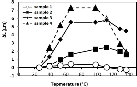
As the first step, we conducted a series of experimental measurements to evaluate impacts on CTE of a thin graphite film by adding Sn layers with different thickness on both sides of its surfaces. Four test coupons of tin-on-graphite were fabricated, numbered #1 to 4. The geometries of the four test coupons are listed in Table 3. Sample #1, 2, 3 and 4 are about 26mm in length.
Table 3 Tested samples from Teledyne Scientific. Test Coupons Graphite Thickness
(µm)
Tin layer Thickness (µm)
1 120 0
2 120 0.5
3 120 1
4 120 2
Fig. 10 shows sample appearances. The thickness for all TIM samples ranges from 0.12mm to 0.2mm.
Fig. 10 TIM samples. The red arrow represents the CTE measuring direction.
Fig. 11 Averaged linear expansion of TIM sample #2.
A typical measurement of TIM samples is shown in Fig. 11. Each point in the figure represents an average from three different experimental results. The upper and lower ends of each bar represent maximum and minimum linear expansion, respectively, at its corresponding temperature. All four samples were characterized three times and averaged. The corresponding thermal changes are shown in
Fig. 12. The averaged CTE is calculated from each temperature segment. For example, there are seven CTEs for the adjacent temperature points in each independent experiment as any temperature differences can be served as a ΔT in Eq. 1. The temperature range during CTE measurement is from 25°C to 137°C.
Fig. 12 Linear expansion of TIM samples #1, #2, #3 and #4.
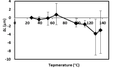
Two thicker graphite-tin TIM samples (#5 and #6, both are ~0.2mm in thickness) were tested as well. Unlike samples #1 to 4, these TIM samples have a vertical-oriented multi-layered structure, in which graphite and tin solder layers are laminated (Fig. 13). The CTE measurement was executed along z-direction. The samples have a graphite-to-solder ratio of 10:1. The thermal expansion of samples #5 and #6 are shown in Figs 14 and 15, respectively. Each sample is tested three times and averaged.
Fig. 13 TIM sample with 10:1 graphite-to-solder ratio.
Fig. 15 Linear expansion measurement of sample #6.
Table 4 Summarizes the CTEs and the corresponding lengths of six TIM samples. For sample #1, #2, #3 and #4, only data below 100°C is calculated, in order to better demonstrate the effect of the tin layers added to the samples and avoid the unusual CTEs with negative trends.
Table 4 Summary of CTEs for TIM samples.
Sample # Sample length (mm) Averaged CTE (/°C)
1 26.46 0.28×10⁻⁶
2 24.87 0.62×10⁻⁶
3 26.12 2.93×10⁻⁶
4 26.9 5×10⁻⁶
5 14.86 -0.267×10⁻⁶
6 14.75 -0.225×10⁻⁶
When coming to TIM samples, they perform quite differently from ordinary materials (e.g. pure copper and pure silicon tested in this research). For samples #1 to #4, they expanded quite linearly during heating when temperatures are below 100°C. It can be observed that the decreasing trend of CTEs below 100°C is highly correlated with the ratios of composition of graphite films and metal layers. The averaged CTEs show a clear trend in Fig. 16 and follow the mechanics of composite and indicate that we can readily modify CTEs of regular solder by laminating solder layers with aligned graphite films, which will also significantly enhance thermal transport of the solder due to high in-plane thermal conductivity of graphite films. When temperatures are over 100°C, the samples begin to shrink. The phenomena of negative CTE is unusual, assumabily due to the special design on graphite micro-structures.
Fig. 16
Samples of #5 and #6 were from the same bigger sample and cut from different spots. The composition structures are vertically oriented, as demonstrated in Fig. 13, different from #1 to #4 with single graphite layer. Higher solder contents are expected to provide better comformability to surface roughness for the molten state of solder during the bonding process. Test results for #5 and #6, whose multiple tin layers are laminated among graphite films, show zero expansion. This indicates that CTE of a TIM is highly dependent on its structure besides its material composition and further investigation, especially from the microstructure and manufacture point of views, is needed.
4. CONCLUSIONS
An optical CTE measuring system was developed and validated by taking CTE measurements on Copper Alloy 101 and pure silicon. Such validation matches well with published literature when temperatures of the samples are within the room temperature and 150°C. Our CTE measurement stops at 150°C because the TIM samples start softening and melting over 200°C. This defines our measuring temperature range within ~120°C. Longer samples may improve the accuracy by increasing ΔL when temperature changes. On the other hand, future application of automatic focusing and computer-based image processing may eliminate the subjective judgment made by human eyes.
We successfully developed a new approach of fabricating CTE-adjustable TIMs and measured their corresponding CTEs. We observed unique characteristics on CTEs of the new TIMs. Reasons for (a) negative overall CTEs, and (b) positive CTEs below 100°C and negative CTEs over 100°C, observed in TIM samples are still unclear. However, it is proven that the new type of TIMs can be designed to match the CTE for targeted bonding materials. By plating metal layers on graphite films, CTEs for TIMs can be tuned from 0 to 5×10⁻⁶/°C. Also, the laminated structures of the TIMs can significantly reduce the CTEs of the TIMs.
This unique CTE-matching feature of a bonding material will have great potential to impact the future development of high heat flux, high power microelectronics devices.
ACKNOWLEDGEMENTS
The authors gratefully acknowledge the contracts from DARPA (N66001-09-C-2015). The views expressed are those of the authors and do not reflect the official policy or position of the Department of Defense or the U.S. Government. In the event permission is required, DARPA is authorized to reproduce the copyrighted material for use as an exhibit or handout at DARPA-sponsored events and/or to post the material on the DARPA website. The authors also appreciate Tony Liao from Teledyne Scientific for preparing TIM samples.
REFERENCES
Amama, P. B., Ogebule, O., Maschmann, M. R., 2006, "Dendrimer-Assisted Low-Temperature Growth of Carbon Nanotubes by Plasma-Enhanced Chemical Vapor Deposition," Chemical Communications (Cambridge England), (27), 2899-2901.
http://dx.doi.org/10.1039/B602623K
Balandin, A. A., 2011, "Thermal Properties of Graphene and Nanostructured Carbon Materials," Nat Mater, 10 (8), 569-581.
http://dx.doi.org/10.1038/nmat3064
Balandin, A. A., Ghosh, S., Bao, W., 2008, "Superior Thermal Conductivity of Single-Layer Graphene," Nano Letters, 8 (3), 902-907.
http://dx.doi.org/10.1021/nl0731872
Biercuk, M. J., Llaguno, M. C., Radosavljevic, M., 2002, "Carbon Nanotube Composites for Thermal Management," Applied Physics Letters, 80 (15), 2767.
Boccaccini, A. R., and Hamann, B., 1999, "Review in Situ High-Temperature Optical Microscopy," Journal of Materials Science, 34 (22), 5419-5436.
http://dx.doi.org/10.1023/A:1004706922530
Choi, S. U. S., Zhang, Z. G., Yu, W., 2001, "Anomalous Thermal Conductivity Enhancement in Nanotube Suspensions," Applied Physics Letters, 79 (14), 2252-2254.
http://dx.doi.org/10.1063/1.1408272
Ganguli, S., Roy, A., and Anderson, D., 2008, "Improved Thermal Conductivity for Chemically Functionalized Exfoliated graphite/epoxy Composites," Carbon, 46 (5), 806-817.
http://dx.doi.org/10.1016/j.carbon.2008.02.008
Hahn, T. A., 1970, "Thermal Expansion of Copper from 20 to 800 K - Standard Reference Material 736," Journal of Applied Physics, 41 (13), 5096-5096.
http://dx.doi.org/10.1063/1.1658614
Neumeier, J. J., Bollinger, R. K., Timmins, G. E., 2008, "Capacitive-Based Dilatometer Cell Constructed of Fused Quartz for Measuring the Thermal Expansion of Solids," Review of Scientific Instruments, 79 (3), 033903-033903.
http://dx.doi.org/10.1063/1.2884193
Okada, Y., and Tokumaru, Y., 1984, "Precise Determination of Lattice Parameter and Thermal Expansion Coefficient of Silicon between 300 and 1500 K," Journal of Applied Physics, 56 (2), 314-314.
http://dx.doi.org/10.1063/1.333965
Prasher, R., 2006, "Thermal Interface Materials: Historical Perspective, Status, and Future Directions," Proceedings of the IEEE, 94 (8), 1571-1586.
http://dx.doi.org/10.1109/JPROC.2006.879796
Raether, F., Springer, R., and Beyer, S., 2001, "Optical Dilatometry for the Control of Microstructure Development during Sintering," Materials Research Innovations, 4 (4), 245-250.
http://dx.doi.org/10.1007/s100190000101
Raza, M. A., Westwood, A. V. K., and Stirling, C., 2010, "Graphite nanoplatelet/silicone Composites for Thermal Interface Applications," Advanced Packaging Materials: Microtech, 2010. APM '10. International Symposium on, 34-48.
http://dx.doi.org/10.1109/ISAPM.2010.5441382
Roberts, R.,B., 1981, "Thermal Expansion Reference Data: Silicon 300-850 K," Journal of Physics D: Applied Physics, 14 (10), L163-L166; L163-L166.
http://dx.doi.org/10.1088/0022-3727/14/10/003
Shahil, K. M. F., and Balandin, A. A., 2012, "Graphene - Multilayer Graphene Nanocomposites as Highly Efficient Thermal Interface Materials," Nano Letters, , 120117152312004.
http://dx.doi.org/10.1021/nl203906r
Tao Tong, Yang Zhao, Delzeit, L., 2007, "Dense Vertically Aligned Multiwalled Carbon Nanotube Arrays as Thermal Interface Materials," Components and Packaging Technologies, IEEE Transactions on, 30 (1), 92-100.
http://dx.doi.org/10.1109/TCAPT.2007.892079
Wang, S., Tambraparni, M., Qiu, J., 2009, "Thermal Expansion of Graphene Composites," Macromolecules, 42 (14), 5251-5255.
http://dx.doi.org/10.1021/ma900631c
Winkler, S., Davies, P., and Janoschek, J., 1993, "High-Temperature Dilatometer with Pyrometer Measuring System and Rate-Controlled Sintering Capability," Journal of Thermal Analysis and Calorimetry, 40 (3), 999-1008.
http://dx.doi.org/10.1007/BF02546859
Yu, A., Ramesh, P., Sun, X., 2008, "Enhanced Thermal Conductivity in a Hybrid Graphite Nanoplatelet - Carbon Nanotube Filler for Epoxy Composites," Advanced Materials, 20 (24), 4740-4744.
http://dx.doi.org/10.1002/adma.200800401
Yu, A., Itkis, M. E., Bekyarova, E., 2006, "Effect of Single-Walled Carbon Nanotube Purity on the Thermal Conductivity of Carbon Nanotube-Based Composites," Applied Physics Letters, 89 (13), 133102.
http://dx.doi.org/10.1063/1.2357580
Zhao, Y., Strauss, D., Chen, Y. C., 2012, "Experimental Study of A High Performance Aligned Graphite Thermal Interface Material," ASME Conference Proceedings.
Zhao, Y., Strauss, D., Liao, T., 2011, "Development of a High Performance Thermal Interface Material with Vertically Aligned Graphite Platelets," ASME Conference Proceedings, 2011 (38921), T30010-T30010-7.