Estimation of the PCB Production Process Using a Neural Network
Kuo-Hsien Hsia
1,
Jr-Hung Guo
2,*1Department of Computer Science and Information Engineering, Far East University, Tainan, Taiwan 2
Department of Electrical Engineering, National Yunlin University of Science & Technology, Yunlin, Taiwan
Received 16 April 2019; received in revised form 16 May 2019; accepted 23 June 2019
DOI: https://doi.org/10.46604/peti.2020.4265
Abstract
Printed Circuit Boards (PCB) are an integral part of all electronic products, and the production process for
printed circuit boards is quite complex. As the life cycle of electronic products becomes shorter and shorter, and the
precision and signal bandwidth of electronic products become higher and higher, the manufacturing process of
printed circuit boards is further complicated. Therefore, how to pre-evaluate the production difficulty before starting
the production will effectively increase the efficiency and quality of printed circuit board production.
Gerber file is the most commonly used data format for the printed circuit board industry. This file contains most
of the parameters required for the manufacture of printed circuit boards. Therefore, this study uses a neural network
to evaluate new PCB products before they are produced through the production parameters that are more influential
in the PCB manufacturing process. This makes it possible to evaluate the difficulty and the required production
process before the new PCB product is produced. This will be very beneficial for the PCB production schedule,
quality control, and cost.
Keywords: printed circuit board (PCB), neural network, Gerber file, production schedule
1.
Introduction
Printed Circuit Boards (PCB) are an essential component of all electronic products. However, due to the complexity of its
manufacturing process and the shortened life cycle of electronic products, the PCB industry must adjust production equipment
and parameters at any time according to the needs of products or customers. In addition, due to the demand for equipment and
processing, the PCB industry often needs to outsource the process or equipment shortage. This makes the entire production
process control, production data collection, quality management, raw materials management, etc., face many problems.
Therefore, how to make these problems and processes be managed and properly arranged will be an important issue for the
PCB industry to continue to survive and grow under international competition.
In previous studies, such as [1], the Hybrid Taguchi Genetic Algorithm (HTGA) was used to optimize the drilling path of
the PCB. [2] used the Modified Artificial Bee Colony Algorithm (MABCA) for the Automatic Nozzle Changer (ANC)
assignment problem, the nozzle assignment problem, and the component pick-and-place sequence problem three problems are
optimized. [3] used image and embedded systems to do PCB defect detection. [4] used a Gerber file as the detection of PAD on
the PCB. From previous studies, we found that there is not much research on PCB production forecasting, mainly because the
previous PCB production mode is mass production. Due to rapid market changes and diversified customer demand, the
manufacturing pattern of printed circuit board products has gradually changed to a “small variety” and “short delivery”
production method. Faced with more and more requests for temporary rush orders and insert orders, how to quickly replace the
production materials and product models under the pressure of limited delivery time. And let the on-site personnel maintain the
quality consistency under the frequent conditions of changing the line, and the production management personnel can quickly
arrange the production line, in line with the customer delivery period, which will be the key to the success of the enterprise
transformation industry 4.0. In order to solve these problems, many manufacturers have introduced MES (Manufacturing
Execution System) and APS (Advanced Planning and Scheduling), but there are not many successful cases. The main reason is
that product information cannot be collected in real time. The problem of not being able to collect production information in
real time is that the production equipment is complicated, or the product information is collected manually, and the data
collection cannot be instantaneous or even wrong. Therefore, if we can obtain the PCB specification data, we can pre-evaluate
its difficulty, even the required time and raw materials, which will greatly help the PCB industry.
The PCB is produced in the PCB factory by the Gerber [5] format file. Because of its simple data format and composition,
and almost every LAYOUT software such as Altium Designer, PADS, Allegro, etc. can output this format, it is widely used in
the circuit board industry. Gerber file is a series of data consisting of X, Y coordinates. These coordinates can indicate the
starting point, end point, PAD position or other special position on the electronic circuit diagram. The Gerber file was
originally a data file exported from the PCB CAD software as an optical drawing language. The format developed by a US
company called Gerber Scientific's professional plotter in the 1960s is now owned by Ucamco. Almost all developments
related to PCB CAD systems are based on this format, and the Gerber file can be directly inputted into the plotter to draw the
negatives required for each station on the board. Therefore, the Gerber file has become recognized in the electronics industry
standard.
Usually, a Gerber file defines a single line layer image, so the PCB manufacturer can get the information needed for
production from the Gerber file of each layer. The Gerber format commonly used in the PCB industry is the RS-274X Gerber
format, also known as the extended Gerber format or X-Gerber, which is a two-dimensional vector graphics description format.
The RS-274X is a readable ASCII format consisting of a series of commands and coordinates. The RS-274X document
contains a complete description of the layers of the board, with all the elements needed for board graphics, and can define any
shape apertures. It can be automatically imported and processed, making it ideal for fast and secure data conversion and
reliable automated workflows.
Therefore, this study hopes to be able to analyze the production difficulty through the neural network when obtaining the
Gerber file and even calculate the precise production time and the required raw materials. Because the production process of
PCBs is very long, this study will focus on the Exposure process in the Etching process. The reason why this process will be
selected as the research goal is that there are more and more layers of PCBs, and the PCB will appear as shown in Fig. 1 due to
design considerations.
(a) PCB examples 1 (b) PCB examples 2
Fig. 1 Two examples of PCBs that are difficult to make
The reason why this process will be selected as the research goal is that there are more and more layers of printed circuit
boards, and the PCB will appear as shown in Fig. 1 due to design considerations. Under normal circumstances, in the etching
process, the larger the area of the remaining copper foil, the shorter the time required for Exposure, so the Exposure time
required for Fig. 1(b) should be relatively short under normal conditions. However, as in the position indicated by the arrow in
exposure time needs to be shortened during exposure. In order to avoid the area where the interval is small, it is enlarged or
completely etched during the etching operation, causing a problem of quality. So how to correctly estimate the exposure time is
very important.
Although Gerber file is a two-dimensional vector graphic description format, Table 1 is a small Gerber file sample, and
Fig. 2 is the actual drawing result. From this example, we can see that the format is only describing the categories of Apertures
as well as the actions and coordinates, not the actual drawing objects. Therefore, it is difficult to know the design of the PCB
directly from the Gerber file. Therefore, this study draws the Gerber file graphically and then uses Convolutional Neural
Networks (CNN) to find the number of smaller pitch areas in the PCB design. The results obtained through such calculations
and analysis can be used to estimate the time required for production. In terms of time estimation, we also use the
Convolutional Neural Networks Method, and the parameters used as input are sample image type, sample image size, time, and
PCB size.
Table 1 Gerber file code sample [6]
G54D16* <-select aperture 6 (20 mil circle trace) G01X90Y85D02* <-move the shutter to 90,85
Y85D01* <-open the shutter and draw to 90,85
X190* <-while shutter remains open, draw to 90,185
Y85* <-draw to 190,85
X90* <-draw to 90,85
G54D45* <-select aperture 45 (60 mil circle flash) X140Y135D02* <-close shutter and move to 140,135
D03* <-flash expose
X0Y0D02*M02* <-return to the origin and Stop
Fig. 2 Gerber file code sample draw result [6]
2.
Convolutional Neural Networks Method
Fig. 3 A simple convolution Net [7]
In this study, we used the Convolutional Neural Networks Method, which is commonly used in many types of neural
networks for image recognition and image processing. The advantage is that it can be converted from the point in the image to
the comparison of the regions, and then through the judgment of the feature, the stepwise comparison results are superimposed
to find the position with the feature. This comparison process is shown in Fig. 3. How was the Convolution Layer achieved?
Convolution
+ReLU Pooling Convolution +ReLU Pooling
Fully Connected
Fully
Basically, centering on each point in the image, then taking N x N points to form an area, where N is called Kernel Size. The
matrix weight of N x N is called the Convolution Kernel. Because the general image is based on RGB, it is necessary to
separately process the RGB three layers separately, and then superimpose the results of the three layers to obtain the
recognized result. The whole process is shown in Fig. 4.
Fig. 4 Simple convolutional neural networks [8]
However, Convolution has a large amount of computation, so we must first pool the graphics we want to compare.
Pooling is a way to compress images and preserve important information. Pooling selects different windows on the image and
selects a maximum value in the window range. After the original image is pooling, the number of pixels it contains will be
reduced to one-fourth of the original. However, because the pooling image contains the maximum value of each range in the
original image, it still retains the degree of conformity between each range and each feature. In other words, the pooling
information is more focused on whether there are matching features in the image, not where the features exist in the image.
This can help CNNs determine whether a feature is included in the image without having to be distracted by the location of the
feature. In addition, we also added a Rectified Linear Unit (ReLU), which is used to convert all negative numbers on the picture
in the Convolution operation to 0. This technique can prevent the result of CNNs from approaching 0 or infinity.
Although this method can avoid the interference of the noise in the image and the sharpening action of the image.
However, there are still several problems when actually performing image recognition with the Convolutional Neural
Networks Method. The first is how the features of the image should be obtained. This part can be solved by backpropagation,
that is, we can prepare some identification samples in advance. Then, after a lot of training, the Convolutional Neural Networks
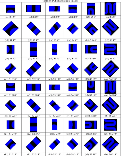
Method can accurately find out whether the feature is in the image and its position. Table 2 shows the sample images we
selected. These 6 samples are more common in PCB design with small line widths, small line spacing, and special designs.
In addition, in order to speed up the training speed and accuracy of the Convolutional Neural Networks Method, we
produce sample images in 45 degrees for each image. Finally, in the resolution part of the sample image, since we have
processed the Gerber file into an image and processed it, and the resolution of the image we draw is 200 dpi, the sampling of all
sample images is also obtained under the same resolution. In terms of time estimation, we use the Long Short-Term Memory
network (LSTM network), and the parameters used as input are the sample image type, the number of sample images, the time,
and the PCB board size. Then use the previous PCB production time in the exposure process and the Gerber file and other
Table 2 6 PCB shape sample images
(a1) S1 0° (a2) S2 0° (a3) S3 0° (a4) S4 0° (a5) S5 0° (a6) S6 0°
(b1) S1 45° (b2) S2 45° (b4) S3 45° (b4) S4 45° (b5) S5 45° (b6) S6 45°
(c1) S1 90° (c2) S2 90° (c3) S3 45° (c4) S4 90° (c5) S5 90° (c6) S1 90°
(d1) S1 135° (d2) S2 135° (d3) S3 135° (d4) S4 135° (d5) S5 135° (d6) S6 135°
(e1) S1 180° (e2) S2 180° (e3) S3 180° (e4) S4 180° (e5) S5 180° (e6) S6 180°
(f1) S1 225° (f2) S2 225° (f3) S3 225° (f4) S4 225° (f5) S5 225° (f6) S6 225°
(g1) S1 270° (g2) S2 270° (g3)S3 270° (g4) S4 270° (g5) S5 270° (g6) S6 270°
(h1) S1 315° (h2) S2 315° (h3) S3 315° (h4) S4 315° (h5) S5 315° (h6) S6 315°
3.
Experimental Results
Since we need to plot the Gerber file, we refer to the GerberView [9] project to draw the Gerber file, and then use C# to
develop the neural network analysis software. And using EMGUCV [10] to process the painted Gerber file into image files and
After the entire software was completed, we used 1000 Gerber files as training samples. We also record the number and
location of six sample images for each Gerber file while training. After training, we found that we set the weight of each sample
in the six sample images to be the same at first, but after training, we found that the sample image weight of the 45-degree
multiple will increase. In addition, if there is less than 3 mil design in the Gerber file, there is a slight influence on the
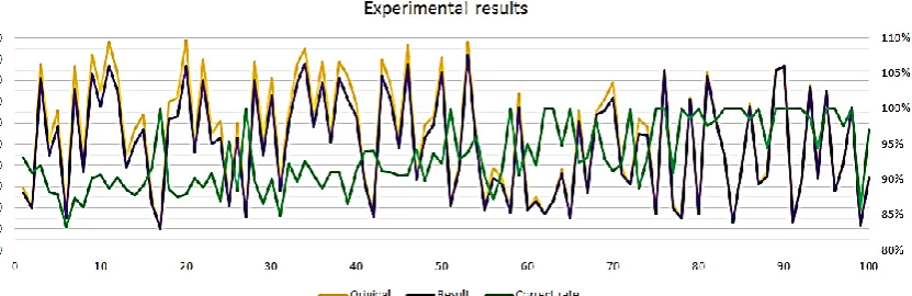
recognition rate. After the identification and statistics of the images, we used the data and the results of the previous production
process to make time prediction training. Then use another 50 Gerber files to estimate the time and compare it with the actual
production results. The results are shown in Fig. 6. From the figure, we can see that the average correct rate is still more than
90%.
Fig. 5 Convolutional neural networks and gerberview software
Fig. 6 Comparison of the estimated time and the actual time
4.
Conclusions
In this study, we used a Gerber file as the basis for PCB production time estimates. Because the Gerber file is a
step-by-step description of the objects on the PCB, rather than a complete representation of each object with 2D data.
Therefore, in this study, the Gerber file is first imaged, and six types of sample images that are difficult in PCB production are
selected, and then identified by CNN. Then, the results of the identification will be trained with the previous production
materials, and the PCB data that have not yet been produced will be used for estimation. After the actual test, the estimated time
and the actual time correct rate is on average more than 90%. Therefore, it can be confirmed that this method is effective.
However, during the experiment, some PCB special designs were still found, which would have a bad effect on the results. In
the future, we will continue to use the CNN method to directly analyze the Gerber file, hoping to improve the results of the
entire identification and prediction. And let this result extend to more PCB processes, and even the production quality and
other information will be added in the future. And let this result extend to more PCB processes, and even the production quality
Conflicts of Interest
The authors declare no conflict of interest.
References
[1] D. H. A. Janan and T. K. Liu, “The optimization of CNC PCB drilling using hybrid taguchi genetic algorithm,” Kybernetes, vol. 45, no. 1, pp. 107-125, 2016.
[2] C. J. Lin and M. L. Huang, “Modified artificial bee colony algorithm for scheduling optimization for printed circuit board production,” Journal of Manufacturing Systems, vol. 44, pp. 1-11, July 2017.
[3] N. Dave, V. Tambade, B. Pandhare, and S. Saurav, “PCB defect detection using image processing and embedded system,” International Research Journal of Engineering and Technology, vol. 3, no. 5, pp. 897-1901, 2016.
[4] V. Raghuvanshi, A. Burman, P. P. Bartakke, and S. Deshpande, “PCB solder pad inspection mechanism using gerber file,” 2016 International Conference on Communication and Signal Processing (ICCSP), IEEE, April 2016.
[5] “Gerber Formats,” https://www.ucamco.com/en/guest/downloads, February 8, 2019.
[6] “Gerber Translator,” http://literature.cdn.keysight.com/litweb/pdf/ads2008/trans/ads2008/Gerber_Translator.html, March 26, 2019.
[7] “An Intuitive Explanation of Convolutional Neural Networks,”
https://ujjwalkarn.me/2016/08/11/intuitive-explanation-convnets/, March 26, 2019.
[8] “Convolutional Networks,” http://cs231n.github.io/convolutional-networks/, March 26, 2019. [9] “Gerber View,” https://sourceforge.net/projects/gerberview/, March 2, 2019.
[10] “EMGU CV,” http://www.emgu.com/wiki/index.php/Main_Page, January 8, 2019.
Copyright© by the authors. Licensee TAETI, Taiwan. This article is an open access article distributed under the terms and conditions of the Creative Commons Attribution (CC BY-NC) license
![Fig. 2 Gerber file code sample draw result [6]](https://thumb-us.123doks.com/thumbv2/123dok_us/9832236.1969391/3.595.149.448.256.553/fig-gerber-file-code-sample-draw-result.webp)
![Fig. 4 Simple convolutional neural networks [8]](https://thumb-us.123doks.com/thumbv2/123dok_us/9832236.1969391/4.595.156.434.124.388/fig-simple-convolutional-neural-networks.webp)