Jyotibhusan Padhi et al, International Journal of Computer Science and Mobile Applications, National Conference on “The Things Services and Applications of Internet of Things”, Gandhi Institute for Education and Technology (GIET) Baniatangi, 23-24 March 2018, pg. 56-62
ISSN: 2321-8363 Impact Factor: 5.515
DESIGN OF A WIDEBAND TWO-LAYER
PATCH ANTENNA FOR IOT APPLICATIONS
Jyotibhusan Padhi
1, Madhulita Mohapatra
2, Suraj Kumar Samal
31
Assitant professor, GIET, Bhubaneswar, [email protected]
3Assitant professor, GIET, Bhubaneswar, [email protected]
3Assitant professor, GIET, Bhubaneswar, [email protected]
Abstract
In this paper, a new design of a Wideband two-layer patch antenna with bandwidth characteristics is proposed. The antenna consists two patches one is driving element and another one is radiating element. The radiating patch is further improved to enhance the bandwidth of the proposed antenna. The fractal concept is followed to enhance the bandwidth of the antenna. Sierpinski Carpet concept is followed to improve surface current density on the radiating element. With this design the return loss response is found to be below -10dB with the frequency range of 5.2 GHz to 5.87 GHz with this the antenna radiates electromagnetic waves uniformly over the frequency band. As this antenna operating from 5.2 GHz to 5.87GHz, it is a suitable candidate for IoT applications.
Keywords:Bandwidth; Ground plane; electromagnetic waves; Slotted rectangular patch
1. Introduction
In today’s world antenna plays a major role in wireless communication, due to its vast use in devices like- mobile phones, GPS systems, mp3 players etc. The antenna is a device i.e. used for efficient transmission and reception of electromagnetic waves. Depending upon the use, the antenna can operate in different frequency bands. In this paper, a wideband two layer patch antenna is designed with improved bandwidth in C- band i.e. ranging from 5.2GHz to 5.8GHz. C-band is mainly used where clarity and quick response is very much essential like in satellite communication, Wi-Fi, vehicular and IoT applications etc.
Among the different types of antenna present nowadays, a lot of research is going on microstrip antenna because of its advantages like- low cost, lightweight, compatibility for an embedded antenna in handheld wireless devices [1-3] and high performance. The main problem in this antenna is narrow bandwidth. Y. Sung and co. suggested an idea to enhance the bandwidth of the antenna by introducing parasitic centre patch [4]. Moreover some planar antenna has been introduced Sierpinski carpet fractal concept to improve the performance of the antenna [5-6].
The bandwidth of an antenna is inversely related to patch area; hence by loading different slots the area can be minimized as a result, bandwidth can be improved [7-8]. The objective of this paper is to improve the bandwidth of microstrip antenna by multi layering the patches and by introducing fractal concept on the radiating element.
Jyotibhusan Padhi et al, International Journal of Computer Science and Mobile Applications, National Conference on “The Things Services and Applications of Internet of Things”, Gandhi Institute for Education and Technology (GIET) Baniatangi, 23-24 March 2018, pg. 56-62
ISSN: 2321-8363 Impact Factor: 5.515
2. Antenna Design and Specification
The basic steps for the development of antenna are given below. The thickness of dielectric material, width and length of the patch, extension length of radiating patch is first calculated before designing the antenna using the following mathematical expressions.
Thickness of the dielectric medium is given as:
(1)
Width of the radiating patch is as follows:
(2)
Length of metallic patch is calculated as:
(3)
Where
: Velocity of light m/s : Dielectric constant of the substrate
: Resonant frequency of antenna
(4)
Extension length of the radiating patch is as:
(5)
Jyotibhusan Padhi et al, International Journal of Computer Science and Mobile Applications, National Conference on “The Things Services and Applications of Internet of Things”, Gandhi Institute for Education and Technology (GIET) Baniatangi, 23-24 March 2018, pg. 56-62
ISSN: 2321-8363 Impact Factor: 5.515
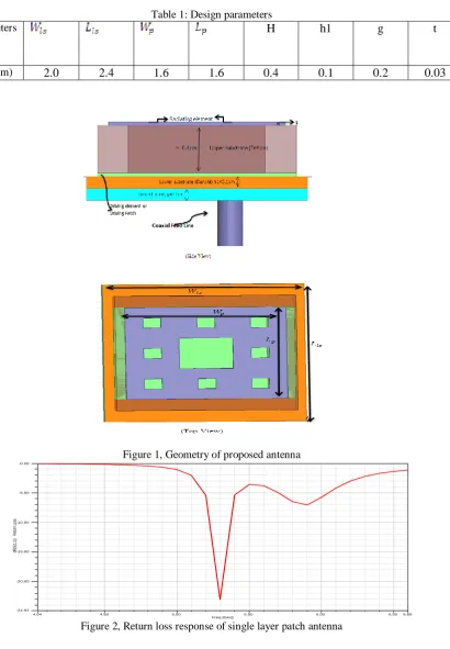
Table 1: Design parameters
Parameters H h1 g t
Unit(cm) 2.0 2.4 1.6 1.6 0.4 0.1 0.2 0.03
Figure 1, Geometry of proposed antenna
4.04 4.50 5.00 5.50 6.00 6.50 6.60 Freq [GHz]
-24.92 -20.00 -15.00 -10.00 -5.00 -0.08
dB(S
(1
,1
))
R
et
urn
L
oss
Jyotibhusan Padhi et al, International Journal of Computer Science and Mobile Applications, National Conference on “The Things Services and Applications of Internet of Things”, Gandhi Institute for Education and Technology (GIET) Baniatangi, 23-24 March 2018, pg. 56-62
ISSN: 2321-8363 Impact Factor: 5.515
2.01 3.00 4.00 5.00 6.00 7.00 7.74 Freq [GHz]
-24.76 -20.00 -15.00 -10.00 -5.00 0.00
dB(S
(1
,1
))
R
et
urn
L
oss
m1 m2 Name X Y
m1 5.3000-19.4854 m2 5.7000-24.5145
Figure 3, Return loss vs. frequency response of modified antenna
3. Result and Discourse
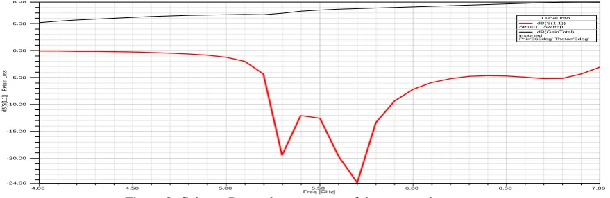
The proposed two-layer patch antenna is simulated using HFSS software. The return loss of microstrip antenna before modification is shown in fig 2 and from figure 3 it is observed that the return loss response of the two-layer proposed antenna with a modified radiating element. The return loss is below -15 dB which is much better than the unmodified antenna. As the return loss is very low, it shows proper impedance matching in between patch and feed. The bandwidth of the designed antenna is 0.67GHz ranging from 5.2GHz-5.87GHz and getting two notches at 5.3GHz and 5.68 GHz within the frequency band.
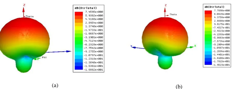
The 3D radiation patterns of the designed antenna at different frequencies are shown in fig 4 and it is observed that it radiates electromagnetic waves are propagating maximally in the upper hemisphere of the patch. The antenna is more directive in the forward direction with a minimum back loop. Fig.5 depicts its 2D radiation pattern in H-plane. From figure 6, it is observed that the antenna offers directional radiation pattern in the operating range. The voltage standing wave ratio of the proposed antenna is depicted by fig.7.The VSWR is found to be less than 2.15 in the frequency range ranging from 5.2GHz to5.87GHz and it indicates that antenna is properly matched over the operating range. The designed antenna shows a flat gain variation over the operating range as shown in fig.8. The surface current distribution over the radiating patch is shown in fig.9.The current density of the patch is increased by inserting Sierpinski carpet structure on the radiating element.
Figure 4, 3D radiation pattern of proposed antenna at (a) 5.3GHz and (b) 5.8GHz
Jyotibhusan Padhi et al, International Journal of Computer Science and Mobile Applications, National Conference on “The Things Services and Applications of Internet of Things”, Gandhi Institute for Education and Technology (GIET) Baniatangi, 23-24 March 2018, pg. 56-62
ISSN: 2321-8363 Impact Factor: 5.515
Figure 5, 2D Radiation Pattern of designed antenna in H-plane ( )
-200.00 -150.00 -100.00 -50.00 0.00 50.00 100.00 150.00 200.00 Theta [deg]
0.00 5.00 10.00 15.00 20.00 25.00 30.00
dB(r
ET
ot
al
)
Curve Inf o dB(rETotal) Setup1 : Sw eep Freq='5.5GHz' Phi='0deg'
dB(rETotal)_1 Imported Freq='5.7GHz' Phi='0deg'
dB(rETotal)_2 Imported Freq='5.5GHz' Phi='0deg'
dB(rETotal)_3 Imported Freq='5.3GHz' Phi='0deg'
Figure 6, Radiation pattern for different frequency vs. theta
4.76 5.00 5.25 5.50 5.75 6.00 6.25 6.50 6.75
Freq [GHz] -1.99
0.00 5.00 10.00 15.00 20.00 25.00 29.80
VS
WR
(1)
Curve Inf o V SWR(1) Setup1 : Sw eep
Jyotibhusan Padhi et al, International Journal of Computer Science and Mobile Applications, National Conference on “The Things Services and Applications of Internet of Things”, Gandhi Institute for Education and Technology (GIET) Baniatangi, 23-24 March 2018, pg. 56-62
ISSN: 2321-8363 Impact Factor: 5.515
4.00 4.50 5.00 5.50 6.00 6.50 7.00 Freq [GHz]
-24.66 -20.00 -15.00 -10.00 -5.00 -0.00 5.00 8.98
dB(S
(1
,1))
R
etu
rn
Lo
ss
Curve Inf o dB(S(1,1)) Setup1 : Sw eep
dB(GainTotal) Imported
Phi='360deg' Theta='0deg'
Figure 8, Gain vs. Return loss response of the proposed antenna
4. Conclusion
The proposed two-layer patch antenna is simulated successfully using HFSS software and the parameters of the antenna have been examined for an ideal design. The overall dimension of the antenna is 2cm*2.4cm*1cm. Moreover, by adding the Sierpinski carpet structure on the radiating patch improves the frequency bandwidth as well as the performance of the antenna. After simulation, it is observed that the proposed antenna has directional radiation pattern and smooth gain variation over the frequency range. As the antenna is operating from 5.2GHz to 5.87 GHz, the two-layer patch antenna is preferred for Wi-Fi, IoT sensor employment, and other C-band applications.
References
[1] Kumar, Girish, Ray, K.P.:’Broadband microstrip antennas’, (Artech House, Norwood, MA, 2003,1st edn.)
[2] Jyotibhusan Padhi,Muktikanta Dash,Shaktijeet Mahapatra,:’’Design of a corrugated Microstrip Patch antenna with Modified Ground Plane’’,ICCSP April 6-8 ,2016.
[3] Sandip Ghosal,Sekhar Ranjan Bhadra Choudhuri,”Analysis of a rectangular slot on a microstrip Patch antenna with an Equivalent Circuit model”,2013 IEEE.
[4] Y. Sung, “Bandwidth enhancement of the microstrip line fed printed wide slot antenna with a parasitic centre patch,” IEEE Trans. Antenna Propag. vol. 60, no. 4, April 2012.
[5] Y. F. Liu, K. L. Lau, Q. Xue, and C. H. Chan, “Experimental Studies of Printed Wide-Slot Antennafor Wide-Band Applications” , IEEE Antennas and Wireless Propagation letters, Vol. 3, 2004.
[6] C. Y. Huang, W. C. Hsia, and J. S. Kuo, “Planar ultra-wideband antenna with a band-notched characteristic,” Microwave Optical Technology Letters, vol. 48, no. 1, pp. 99–101, 2006.
[7] C. Y. Hong, C. W. Ling, I. Y. Tarn, and S. J. Chung, “Design of a planar ultrawideband antenna with a new band-notch structure”, IEEE Trans.Antennas Propag., vol. 55, no. 12, pp. 3391–3397, Dec. 2007.
[8] K. Shambavi, Zachariah C Alex, “Design of Printed Multistrip Monopole Antenna for UWB Applications”, Microwave and Optical Technology Letters, vol. 53, No.8, pp. 1570-1572, Aug 2011.
Jyotibhusan Padhi et al, International Journal of Computer Science and Mobile Applications, National Conference on “The Things Services and Applications of Internet of Things”, Gandhi Institute for Education and Technology (GIET) Baniatangi, 23-24 March 2018, pg. 56-62
ISSN: 2321-8363 Impact Factor: 5.515
[10] R.G.Hohlfeld, Nathan Cohen, “Self-similarity and Geometric requiremnets for Frequency independence in antenna”, World Scientific Publishing Company, Fractals, Vol. 7,No. 1, 79-84 [11] R G. Hohlfeld , Nathan Cohen , “Self-similarity and the Geometric requirements for
Frequency independence in antennae”, World Scientific Publishing Company, Fractals, vol. 7, No. 1 79-84.
[12] Steven R. Best, “On the Resonant Properties of the Koch Fractal and Other Wire Monopole Antennas”, IEEE Antennas Wireless Propag. Lett, vol. 1, 2002.
[13] Basil Jeemon, K Shambavi, and Zachariah C Alesx, “A multi fractal antenna for WLAN and WiMAX application”,ICT-2013, 978-1-4673-5758-6/13/$31.00 © 2013 IEEE 953.
[14] Ayachi Ajey, Shambavi K, Zachariah C Alex, “Design and Analysis of Fractal Antenna for UWB Applications”, IEEE Students’ Conference on Electrical, Electronics and Computer Science,2012.
A Brief Author Biography
1st Jyotibhusan Padhi – Received the B.Tech. degree in Electronics and Telecommunication Engineering from the University of BPUT, Odisha, in 2013, and the M. Tech. degree in Electronic and Communication Engineering from the University of SOA, Bhubaneswar, Odisha, in 2016. Currently, He is an Assistant Professor of Electronics and communication engineering at Gandhi Institute for Education and Technology. His teaching and research areas include Antenna and Microwave Engineering. Asst. Professor Jyotibhusan Padhi may be reached at [email protected].
2nd Madhulita Mohaptra – Received the B.Tech. degree in Electronics and Telecommunication Engineering from the University of BPUT, Odisha, and the M. Tech. degree in Electronic and Communication Engineering from the University of BPUT, Bhubaneswar, Odisha. Currently, He is an Assistant Professor of Electronics and communication engineering at Gandhi Institute for Education and Technology. His teaching and research areas include Antenna and Microwave Engineering. Asst. Professor Madhulita Mohapatra may be reached at [email protected].
3rd Suraj Kumar Samal – Received the B.Tech. degree in Electronics and Communication Engineering from the University of BPUT, Odisha, in 2013, and the M. Tech. degree in Electronic and Communication Engineering from the KIIT University, Bhubaneswar, Odisha, in 2017 . Currently, He is an Assistant Professor of Electronics and communication engineering at Gandhi Institute for Education and Technology. Asst. Professor Suraj Kumar Samal can be contacted at
![Figure 7, VSWR response of the proposed antenna Freq [GHz]5.75](https://thumb-us.123doks.com/thumbv2/123dok_us/9826869.1968751/5.595.82.521.275.482/figure-vswr-response-proposed-antenna-freq-ghz.webp)