Impact of Annealing on Structural and Optical
Properties of CoPc Thin Films
HuSAm m. El-NASSEr
Department of Physics, Al al-Bayt University, Mafraq 130040, Jordan. http://dx.doi.org/10.13005/msri/120103
(Received: April 28, 2015; Accepted: May 15, 2015) AbSTrACT
The structural and optical properties of four samples of cobalt phthalocyanine (CoPc) thin films having almost the same thickness deposited onto silicon substrates by organic molecular beam deposition (OMBD) were investigated. The intensity distributions of the X-ray diffraction (XRD) patterns confirm the crystalline nature of the films and presents a single sharp dominant peak at 2q=6.9o (d=12.72 A0) of the a-CoPc phase unit cells, which indicates to a preferential orientation (200)
direction, then undergoes a phase transition into b- form in a preferential orientation (001) direction after annealing at 250 and 350°C. Furthermore it was shown that an increasing in the crystallite size (L) occurs upon annealing. The small values of the roughness (7.04 nm, 7.2 nm) obtained from atomic force microscopy (AFM) measurements show relatively smooth and flat surfaces. Despite the identity of the samples deposition conditions, the post growth annealed films show different morphological features of a mean grain size about of 11-26 nm. The optical energy gap was estimated from the absorption coefficient using Tauc’s relation.
Key words: Optical properties, CoPc thin films, surface morphology, UV-VIS spectroscopy, organic thin films.
INTrOduCTION
Organic semiconductors, such as metal phthalocyaninesm (MPcs) have gained much research attention in the development of photodetectors, organic transistors, sensitive gas sensors, and flexible solar cells1-5. Metal
phthalocyanines exhibit thermal stability, chemical inertness, high molecular symmetry, and favorable optical properties. Besides, MPcs can be easily sublimed in high vacuum resulting relatively pure thin films with good growth properties and chemical stability6. Furthermore, the structural properties of
these thin layers can be manipulated intentionally by controlling the substrate temperature or post growth annealing. This will lead to modifying the film phase and the film morphology as well. Modifying the properties plays a crucial role in a wide range of current and future applications including: photovoltaic solar cells, organic light emitting diodes, and organic thin film transistors7-11.
In addition the optical properties of MPcs thin layers were intensively investigated since they are classified as small organic molecules and many factors such as the interaction with the substrate type, its surface, the deposition rate, and the deposition temperature may influence changes in grain size of crystallites and accordingly in structural and optical properties. Therefore, most of MPcs have optical bands labeled with five transition bands Q, B, N, L, and C, and the corresponding energies were identified about 2, 3.6, ,4.4, ,5, and 5.9 eV12.
However, not only MPcs may miss one or two of these bands, but also the absorption line shapes vary from case to case13.
Recently, the organic semiconductor cobalt phthalocyanine (CoPc) has been studied as a promising material for organic light emitting devices (OLED) and organic based solar cells (OSC)14, 15.
together in a crystal forming column like structure. However, few studies have addressed CoPc in terms of its molecular orientation and structure as a function of the substrate temperature15.
In the current work, the ultimate goal is to study the influence of substrate heating during evaporation and post growth annealing on structural and optical properties of CoPc organic thin films using X- ray diffraction (XRD), atomic force microscopy (AFM), and ultraviolet and visible (UV-VIS) spectroscopy.
ExPErImENTAl
CoPc thin films were prepared by organic molecular beam deposition (OMBD) using ultra high vacuum system. The films were deposited on silicon (100) and glass substrates for structural and optical measurements, respectively. The silicon and glass substrates were carefully cleaned by standard methods16. The material was sublimated
from Al2O3 crucible in a vacuum of 10-8 mbar during
the deposition. The rate of deposition was controlled at 0.5 °A/s /s using a quartz crystal microbalance. In addition the annealing of CoPc films was performed at 250 and 350°C for 3 h under argon atmosphere. Besides, the structural characterizations were performed at room temperature using X-ray diffraction (XRD) (Philips X’Pert system) with Cu Ka radiation of quasimonochromatic wavelength 0.15418 nm in the range of 2q between 5° and 60°. Then, the surface morphology was visualized with a Nanoscope IIIA atomic force microscope (AFM), which operates in the tapping mode in air at room temperature. A scanner, equipped with a Si cantilever was used to obtain surface morphology of CoPc films. In order to remove the background slope the images have been processed using the linear flattening method. The Gwyddion software was used for analyzing the AFM images.
Furthermore, the transmittance, T(l) and reflectance at an incident angle of 5°, R(l) spectra of CoPc thin films were performed at room temperature over the spectral range 200–1100 nm using Perkin- Elmer spectrophotometer (Lambda 25) with uncertainty around 1% given by the manufacturer for the measurements obtained by this spectrophotometer. It is worth pointing out, that
a blank glass substrate identical to the ones used for the thin film deposition was used as a reference for the transmittance scan and for calibration purposes. The reflectance scan was taken at normal incidence with aluminum mirror as a reference.
rESulTS ANd dISCuSSIONS
Structural and morphological studies
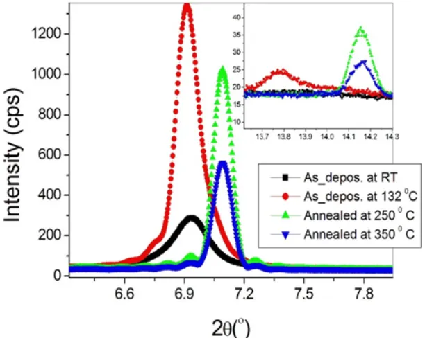
Fig. 1 shows X-ray diffraction patterns for CoPc thin films deposited on silicon substrates prepared with different thermal treatments. The deposited film on the substrate at temperature of 132 0C have an XRD spectra characteristic for
the a-CoPc phase unit cells. Whereas, the a-axis perpendicular to the substrate surface, b and c parameters lie in the substrate plane, with 2q values of 6.90 and 13.80 due to diffraction from the (200)
and (400) planes, respectively. These peaks arise from the interlayer spacing of tilted molecules stack. It is clearly to notice that the intense peak 2q values occurs at 6.90 for the sample prepared at substrate
temperature of 1320C during deposition, this is
a good indication that the deposition conditions have a significant impact on the achieved angle for CoPc molecules, as the energy of these molecules on the surface depends mainly on this parameter. Moreover, annealing films into 250 and 3500C will
have a phase transition from a to b phase crystallites. Accordingly, the peak shifts into a position around 7.090 and 14.20due to diffraction from (001) and (400)
planes, respectively17-20. Furthermore, it is important
to note that the peaks, which originated at 14.20
for the annealed sample at 2500C, is more intense
compared to the annealed sample at 3500C. This
could be attributed to the fact that the a structure is formed when CoPc molecules are grown at these temperatures. Furthermore, the mean crystallite size (L) as a function of the film thickness can be estimated from the half width value of the X-ray diffraction peak, using Scherrer’s equation21:
Fig. 2: AFm images for CoPc thin films deposited on silicon substrates before and after annealing crystallite size L and the distance between the atomic
planes d are given in Table 1.These values are in a good agreement with previously reported results for several phthalocyanine thin films23.
In order to correlate the morphology of CoPc thin film with the crystal structure changes upon thermal treatment AFM was used for the samples before and after annealing. AFM images used to confirm the strong dependence of film morphology on temperature. Whereas, the film deposited at room temperature has planer terraces with pointed heads more oriented perpendicular to the film plane, refer to Fig. (2a). In addition, an elongation of grains was
observed in the form of well interconnected areas in a vermicular-like surface topography as shown in Fig.(2b). This could be attributed to the high diffusive mobility of CoPc molecules at substrate temperature of 1320C. Furthermore, the distances between the
vermicular hill tops of these distinct areas were found to be similar over the whole image. This is a good indication that not only the arrangement of aCoPc molecules is the same but also the a- phase crystallites is the same as well, refer to Fig.2 (a). These areas were transformed upon annealing at 2500C and 3500C into a lamellar like arrays more
oriented parallel to the planes of the films (Fig. 2(c, d)). Besides, as the temperature increase, it is clearly
Table1: Observed parameters of the x-ray pattern of CoPc thin films
Sample As_depos. at rT As_depos. at 132 0C Annealed at 250 0C Annealed at 350 0C
2q(deg.) 6.9 6.9 7.1 7.1
d(nm) 1.272 1.277 1.245 1.245
L(nm) 35.01 56.02 84.02 70.01
to notice the decrease in the film roughness as well as the growth of the grain sizes refer to Fig. 2. While the diameter of drains was found to be around 11-27 nm, the relative roughness was decreased upon annealing from 7.2 to 7.04. This decrease of lateral grain size is directly related to the formation of smaller crystallites at higher temperatures. Whereas, the main parameters (the amount, size, and even orientation) of these arrays indicate that, the á into â transition has been proceeded. Therefore, XRD and AFM measurements give an ability to evaluate CoPc thin films microstructure24-26.
Optical properties
The optical absorption coefficient (a) of CoPc thin films as a function of incident wavelength over the range 400-800 nm were represented in Fig. 3 . Whereas, CoPc thin films present relatively
high optical absorption coefficient at wavelength range about (2.3- 2.7) x 105cm-1. This result is in
a good agreement with several published results [23,27]. Besides, both the deposited film and the one prepared under the substrate temperature (132 0C) show no effect of the substrate temperature
on the absorption coefficient values. This is a good confirmation that the spectra of these two samples are characteristic for the same aCoPc phase. Moreover, the Q-band existed for the same wavelength range, is consisting of two distinct peaks. While the lower wavelength peak at 613 nm is related to Qy band as a result of a1u(p) →eg(p*) transition, the
higher wavelength at 687 nm has been attributed either to the Qx as a result of exitonic transition or to the vibrational interval28-31. Furthermore, as in Fig.
(3), not only the shape of Q-band in the absorption coefficient spectra provides good evidence for
molecular ordering but also the post growing annealing had a significant effect on the variation in the orientation and/or molecules packing within CoPc thin films as a result of phase transition from a to b. Besides, the Davydov’s splitting of the Q-band was observed to decrease from 74 into 70 nm, in which the splitting is proportional to the inverse cube of the molecular separation16. This splitting is a good
indication for that a slight increase in the molecular separation occurred for the samples submitted to post growing annealing at 250 and 3500C for 3h.
Additionally, one can clearly see a slight increase in the relative intensity for higher wavelength peaks of Q-band. This finding is consistent with previously several reported results14, 32.
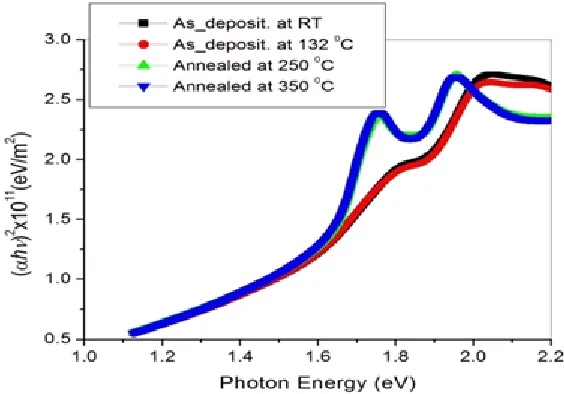
Further analysis regarding the optical properties has been conducted by performing a fit to the exponential part of the spectra. This fit will be a good guide in calculating the optical band gap of CoPc thin films using the Tauc’s equation for allowed direct transition:
...(2) where A is a constant, and Eog is the optical band gap of semiconductor. The band gap was determined by plotting (ahí)2 as a function of
photon energy (hv) (Fig. 5), then the straight line was extrapolated. While the straight line region resemble the energy axis, the intercept at (ahí)2=0 implies the
band gap, refer to Table 2 for more details
The band gap is determined by plotting (ahí)2 as a function of photon energy (hv) (Fig. 5) and
extrapolating the straight line region to the energy axis, and the intercept at (ahí)2=0 implies the band
gap. Table 2 shows the band gap and thicknesses for samples of this work.
CONCluSIONS
In this work, the impact of annealing were investigated. It has been found that annealing has a significant effect on structural, morphological, and optical properties of CoPc thin films deposited Table 2: Values of thickness* and energy
band gap of CoPc thin films before and after annealing.
Sample Thickness(nm) Eg (eV)
As_depos. at RT 86.37 3.099 As_depos. at 132 0C 79.97 3.085
Annealed at 250 0C 80.69 2.763
Annealed at 350 0C 82.11 3.065
*Thicknesses of CoPc thin films were calculated using ellipsometric data
Fig. 4: Plot of (ahí)2 versus photon energy of CoPc thin films before and after annealing in (a)
onto silicon substrates by organic molecular beam deposition. In addition, after annealing a higher crystalline fraction of films were found. Besides, AFM images reveal that a well interconnected uniform particles. Furthermore, with the aid of Tauc’s relation it is found that the appearance of B and Q bands in the absorption spectra indicates that the presence of a1u (p) → eg (p*) transitions of macrocyclic p structure.
Moreover, preparation CoPc thin films and their characterization open up new possibilities not only to control the growth parameters but also to improve the quality of CoPc layers. Finally, the results of this work might be used in designing and fabricating
different technological devices including organic thin film transistors and photovoltaic devices.
ACKNOwlEdgEmENTS
This work was partially supported by the Deutsche Forschungsgemeinschaft (DFG) within project (Wu 243/20-1). The author thankfully acknowledges Al al-Bayt University for the support during the sabbatical leave in the academic year 2013/2014, and wishes to thank organic thin films group at Institute of Physics (IA) RWTH Aachen University, Germany for providing the experimental facilities.
rEFErENCES
1. Wohrle, D.; Meissner, D. Adv. Mater: Organic Solar Cells, 3, 129-138 (1991)
2. Vrkoslav, V.; Jelinek, I.; Matocha, M.; Kral, V.; Dian, J. Mater. Sci. and Eng., C 25, 645-649 (2005)
3. Park, C.; Yun, D. H.; Kim, S. T.; Park, Y. W. Sensors and Actutars: B. Chemical, 30, 23-27 (1996)
4. Wojdyla, M.; Derkowska, B.; Lukasiak, Z.; Waklaw, B. Mater. Lett., 29-30, 3441-3446 (2006)
5. Francia, G. D.; Alfano, B.; Ferrara, V. L. J.of Sensors, 1-18 (2009)
6. Puigdollers, J.; Voz, C.; Fonrodova, M.; Cheylan, S.; Stella, M.; Andreu, J.; Vetter, M.; Alcubilla, R. J. of Noncrystalline Solids, 352, 1778-1782 (2006)
7. Collins, R. A.; Mohammed, K. A J. Phys.D: Appl. Phys., 21, 154-161 (1998)
8. Popielarski, P.; Waklaw, B.; Paprocki, K.; Mosinska, L.; Kowalska, M.; Szybowicz, M.; Makowiecki, J. Electrochem. Acta, 104, 1, 496-504 (2013)
9. Puigdollers, J.; Voz, C.; Fonrodona, M.; Cheylan, S.; Stella, M.; Andreu, J.; Vetter, M.; Alcubilla, R. J of Noncryst.Solids, 352, 1778-1782 (2006)
10. Zhen, L.; Shang, L.; Ming, L.; Ge, L. IEEE Conference on Electron Devices and Solid State Circuits, (2007)
11. Jiguang, D.; Xiaoxia, J.; Haibo, W.; Donghang, Y. Thin Solid Films, 516, 3320-3323 (2008) 12. Abdle-Malik, T. G.; A.A. Ahmed, A. A.; Riad,
A. S. Status Solidi a, 121, 507-513 (1990) 13. Schunemann, C.; Elschner, C.; Levin, A. A.;
Levichkova, M.; Leo, M.; Riede, M. Thin Solid Films, 519, 3939-3945 (2011)
14. Szybowicz, M.; Bala, W.; Dumecke, S.; Fabisiak, K.; Parocki, K.; Drozdowski, M. Thin Solid Films, 520, 623-627 (2011)
15. El-Nahhas, M. M.; Farag, A. A.M.; Atta, A. A. Synthesis Metals, 159, 589-594 (2009) 16. Beigmohamadi, M.;Niyamakom, P.; Farahzadi,
A.; Effertz, C.; Kremers, S.; Brueggemann, D.; Wuttig, M. J. Appl. Phys., 104, 13505 (2008)
17. Lozzi, L.; Santucci, S.; La Rosa, S.; Delly, B.; Picozzi, S. J. Chem. Phys., 121, 1883-1889 (2004)
18. El-Nahhas, M. M.; Abd-El-Rahman, K. F.; Farag, A. A.; Darwish, A. A. Phys. Scr., 73, 40-45 (2006)
19. Schunemann, C.; Elschner, C.; Levin, A. A.; Levichkova, M.; Leo, K.; Riede, M. Thin Solid Films, 519, 3939-3945 (2011)
20. Hassan, A. K.; Gould, R. D. Phys. Status. Solidi A, 132, 91-101 (1992)
21. B. D. Cullity: Elements of x-ray Diffraction. 1977, MA: Addison- Wesley, Boston 22. El-Nahhas, M. M.; El-Gohary, Z.; Soliman, H.
S. Optics and Laser Technology, 35, 523-531 (2003)
23. Pirriera, M. D.; Puigdollers, J.; Voz, C.; Stella, M.; Bertmen, J.; Alcubilla, R. J. Phys. D: Appl. Phys., 42, 145102 (2009)
D: Appl. Phys., 37, 678-688 (2004)
25. Schuster, B. E.; Basova, T. V.; Plyashkevich, V. A.; Peisert, H.; Chasse, T. Thin Solid Films, 510, 7161-7166 (2010)
26. Aziz, F.; Sulaiman, K.; Muhammad, M. R.; Sayyad, M. H.; Karimov, K. World Acad, of Sci., Engineering and Technology, 5, 675-677 (2011)
27. Farag, A. A.; Ashery, A.; Shenashen, M. A. Physica B: Condenced Matter, 407, 2404-2411 (2012)
28. Wojdyla, M.; Derkowska, B.; Lukasiak, Z.; Bala, W. Materials Lett. 60, 3441-3446
(2006)
29. El-Nahass, M. M.; Abd El-Rahman, K. F.; Al-Ghamdi, A. A.; Asiri, A. M. Physica B: Condenced Matter, 344, 398-406 (2004) 30. El-Nahass, M. M.; Farag, A. A. M.; Atta, A. A.
Synthetic Metals, 159, 589-594 (2009) 31. Zawadzka, A.; Polciennik, P.; Czarnecka, I;
Sztupecka, J, Lukasiak, Z. Optical Mater., 34, 1686-1691 (2012)