© Shiraz University
ADAPTIVE NOISE CANCELLATION BASED ARCHITECTURE FOR CORRECTION OF GAIN AND OFFSET MISMATCH
ERRORS IN TIME-INTERLEAVED ADC*
A. KHAKPOUR**, D. ASEMANI AND B. PAPARI
Dept. of Electrical and Computer Engineering, K. N. Toosi University of Technology, Tehran, I. R. of Iran Email: [email protected] , [email protected]
Abstract– Analog-to-Digital Converters (ADCs) represent a main bottleneck for realizing high-speed telecommunication systems such as cognitive radio and Software-Defined Radio (SDR) systems in addition to various requirements of transmission quality. Time-interleaved A-D converter (TI-ADC) may be considered as an effective candidate to achieve high-speed ADC with relatively slow circuits accounting for digital spectrum management. However, mismatch errors cause a considerable degradation in the performance of TI-ADC. In this paper an adaptive compensation technique is proposed for improving the overall performance in presence of offset and gain mismatches. The proposed structure behaves independent from input signal. Here, Least-Mean-Squares (LMS) algorithm has been exploited to adaptively estimate and correct mismatch errors. The Proposed correction method is structurally very simple and hence suitable for implementation on integrated circuits. Besides, proposed digital compensation algorithm is computationally efficient. Considering a four-channel ADC, the proposed compensated TI-ADC provides an approximate improvement of 33.2dB in the performance compared to uncompensated architecture. The proposed compensated TI-ADC would be an efficient high speed ADC in most RF communication applications, and especially applications that deal with tuned frequency.
Keywords– ANC. time-interleaved, mismatch errors, MIMO, wide-band communications
1. INTRODUCTION
High speed and wide-band A/D converters are continuously demanded to account for the requirements of the emerging applications in instrumentations or telecommunications such as Software-Defined Radio (SDR) systems, Cognitive Radio and Digital Video Broadcasting (DVB) [1]. Considering the constraints of practical electronic circuits, a trend in wide-band design exists that tries to overcome performance limitations due to analog errors through digital processing techniques. Nowadays, the performance of A/D converters (ADCs) still cannot fulfill the requirements of the wideband receiver of the SDR approach. Fig. 1 shows a general structure for SDR system. The performance of SDR systems is practically restricted by Digital Signal Processing (DSP) abilities, radio frequency (RF) and antenna subsystems, ADCs, etc. [2, 3]. The demand for A/D or D/A converters with higher speeds has dramatically increased for realizing the new communications concepts such as SDR approach [4]. To achieve higher speeds of conversion, the use of ADCs in parallel has been of interest over several decades [4], [6]. Multiple Input-Multiple Output (MIMO) systems can potentially support very large data rates in wireless systems. In the last few years, researchers have focused on the implementation of MIMO systems with lower hardware complexity, without sacrificing spatial multiplexing gain. To this end, sub-optimal parallel selection methods that
Received by the editors October 18, 2013; Accepted November 26, 2014.
minimize the capacity loss due to MIMO system dimension reduction have been developed [7]. Time-interleaving and discrete-time Hybrid Filter Bank (HFB) ADCs have been proposed to realize a parallel A/D conversion [8, 9].
Fig. 1. General structure of a Software-Defined Radio (SDR) system
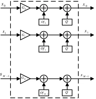
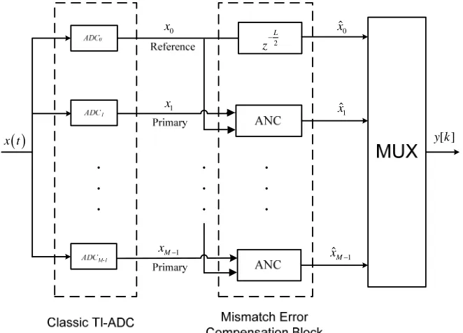
TI-ADC is associated with a parallel ADC structure where there is an ADC at each channel operating at a sampling rate being M-times slower than global TI-ADC clock (Fig. 2). Thus, TI-ADC can be considered as an effective solution to achieve high sampling rate using relatively slow circuits. Main analog input is simultaneously sampled by M branch ADCs considering different clock delays distributed on a global sampling period. The overall sampling rate is, therefore, multiplied by the number of ADCs or branches. Ideally, all channel ADCs should have identical characteristics with the same clock skew [10, 11]. In reality, performance of TI-ADC is influenced by different error terms originated from mismatches occurring among different channels caused by fabrication process variations. Error terms can be decomposed into: offset error, gain mismatch, and timing skew between the channel clocks. In the presence of mismatch errors, the effective output resolution of TI-ADC drastically deteriorates, leading to unacceptable Effective Number of Bits (ENOB). Inter-channel mismatches limit Signal-to-Noise Ratio (SNR) and Spurious-Free Dynamic Range (SFDR) of TI-ADC [12].
[ ]
y k
x t
1
Clk
0
Clk
1 M
Clk
0
Clk
1
Clk
1 M
Clk
S
T
S
M T
Fig. 2. M-Channel TI-ADC architecture. Ts and M represent global clock period and number of
Several compensation techniques have been introduced for correcting gain mismatch errors so far [9-11, 13-16]. Compensation techniques can be categorized according to the digital correction algorithms into adaptive calibration [12] and blind methods [13-15]. Adaptive calibration method proposed in [12] does not require any special information about input signal and can handle the state of slow changes in the mismatch errors but the related structure does not lead to an acceptable accuracy. An adaptive blind method with mixed-domain correction technique has been proposed in [13], taking advantage of each domain to dramatically reduce computational requirements on the digital side. However, it requires additional analogue circuitry. Generalized blind mismatch correction has been investigated for correction of gain mismatch with a simple structure in [14]. However, its computational complexity enlarges the error estimation time. In [15], a method has been employed so that an adaptive blind method is applied to an arbitrary number of channels in a straightforward way, whereas the implementation complexity of the structure linearly grows with the number of channels. Another work [16] tries to compensate frequency-dependent mismatches based on a Discrete Fourier transform (DFT). This approach is limited to a finite number of samples due to DFT calculation and it is not evident how to extend this method to continuous processing of samples.
In this paper, a new adaptive algorithm is proposed as an extension of previous works [13-16]. In previous works, no channel information has been directly exploited. In the proposed method, cross-channel information is explicitly used. Owing to the exploitation of cross-cross-channel information, the proposed method is computationally more efficient in comparison to earlier works [11-15]. Proposed structure aims at compensating offset and gain mismatch errors. For convenience and without loss of generality, simulations are realized using a four-channel TI-ADC in this paper.
In the next section, effects of mismatch error are analyzed in terms of A/D performance. Then section 3 describes the proposed mismatch compensation technique. Section 4 includes the simulation results. Finally, the results are summarized as a conclusion in section 5.
2. ANALYSIS OF MISMATCH ERROR IN TI-ADC STRUCTURE
This section analyzes and studies the effects of mismatch errors in TI-ADC, focusing on gain and offset mismatch. It is supposed that each channel consists of an independent random error in the related gain and offset value whereas other parameters are identical. The mismatch error of each channel is considered separately without any contribution from other branches. To focus on the mismatch errors, the electronic circuit of TI-ADC can be modeled replacing quantization procedure with an additive white noise as shown in Fig. 3.
0
G
0
Of Q
0
s x0
1 G
1
Of Q
1
s x1
1 M
G
1
M
Of Q
1 M
s xM1
For convenience, the complexities of Sample and Hold (S/H) and other electronic parameters have been simply neglected. Now, the effects of gain and offset mismatches on the performance of TI-ADC are analyzed to better follow up the proposed compensation algorithm.
a) Offset Mismatch
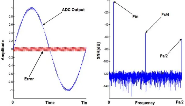
In general, offset mismatch causes a fixed pattern noise appearing in the global ADC output. It is supposed that offset mismatch errors of different channels are independent. Supposing a constant DC input signal, each channel would produce a different output code because of offset errors, leading to a periodic error at the overall output with the period of MTs. This pattern noise is almost independent of the input signal and represents an additive noise in both time and frequency domains as shown in Fig. 4 [18]:
Fig. 4. Offset mismatch error effects on the output of TI-ADC (for a four-channel TI-ADC)
Supposing an M-channel structure, the spectral representation of this noise comprises a series of periodic peaks in frequency domain at the following frequencies [17]:
1 , 2 , . . . S
F
k k
M (1)
This pattern noise in the overall output of TI-ADC is originated from different offset values of channels. In practice, if the offsets at all channels are the same, the pattern noise will converge to simple single-valued (DC) offset error at the overall output. To model the pattern noise due to offset mismatches, the output of each branch of an M-Channel TI-ADC can be described as follows:
[ ]
[ ]
i i i
x
k
s k
o
(2)where
s k
i[ ]
ando
i stand for the ideal value and offset at ith channel respectively. If rth channel is supposed as reference branch, other offsets may be reformulated as:[ ]
[ ]
(
)
i i r i r
x
k
s k
o
o
o
(3)So, if
o
i
o
r is compensated from output of each channel, then a constant offset will remain at all channels as follows:ˆ [ ]
i i[ ]
rwhere
x k
ˆ [ ]
i represent the output of ith channel after eliminatingo
i
o
r. In this case, the whole M-Channel TI-ADC may be modeled as single ADC with a constant offset being equal to the offset of reference branch. As previously mentioned, a constant offset may be compensated easily through standard algorithms.b) Gain mismatch
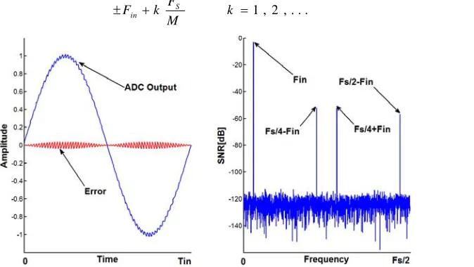
In this section, it is again assumed that the gain mismatches of channels are random and independent, but other parameters are identical. If a sinusoidal input signal is applied to the system, the largest absolute error at the channel outputs occurs at the peaks of the sine wave where the input amplitude is maximal. Thus, a pattern noise due to the gain mismatches appears with a multiplicative form in time domain which behaves like an Amplitude Modulation (AM) noise. This AM noise includes spectral peaks at the following frequencies [17]:
1 , 2 , . . . S
in F
F k k
M
(5)
Fig. 5. The effects of gain mismatch errors on the overall output of TI-ADC (in a four-channel TI-ADC)
where
F
in is the input frequency andF
S represents sampling frequency.In TI-ADC case, the gain errors of channels are independent. Output of each channel of M-Channel TI-ADC can be explained as follows:
[ ] [ ]
i i i
x k s k G (6)
where
s k
i[ ]
andG
i are the ideal output value and gain at ith channel respectively. Supposing rth channel as reference, other gain coefficients may be reformulated as:[ ] [ ] i
i i r
r G
x k s k G
G
(7)
If i r G G
is compensated at the output of all channels, then a similar gain will be applied to all channels as
follows:
ˆ [ ]i i[ ] r
x k s k G (8)
where
x k
ˆ [ ]
i represents the output of ith channel after correcting i r G G. If a suitable correction is
3. PROPOSED METHOD FOR MISMATCH CORRECTION
In this section, an adaptive correction technique is proposed based on Adaptive Noise Cancelling (ANC) to compensate mismatch errors in TI-ADC. To better present the proposed structure, the ANC technique based on LMS algorithm is firstly reviewed. Then, the proposed compensation method is discussed.
a) Adaptive Noise Cancelling Technique
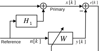
ANC algorithm is a technique for estimating or extracting a signal that is corrupted by an additive noise. Block diagram of the general ANC technique is shown in Fig. 6.
Generally, the ANC algorithm includes two main input signal components: primary signal and reference signal. Primary and reference stand for the noisy signal and input noise respectively. Two known input signals are x[k] and n[k]. Similarly, there are two output signals namely, y[k] and e[k] which are called filter output and error signal respectively. Filter parameters W should be adaptively adjusted so that input noise contribution in error signal e[k] is minimized. By minimizing the signal energy at out of the band of interest, we can adaptively identify the noiseless signal as e[k]. LMS algorithm used to update the filter coefficients, exploits the statistical independence of desired and reference (noise) signals and tries to minimize the output signal energy (error signal) [18].
W
1
H
Primary
Reference
[ ]
x k e k[ ]
[ ] y k
[ ] n k
Fig. 6. General block diagram of Adaptive Noise Cancelling (ANC) method. Primary and reference are desired signal and noise respectively
Error signal is a mixture of primary and filtered signals and hence desired signal and noise. Energy of error signal can be supposed as a linear combination of noise and desired signal, assuming that desired and noise signals are statistically independent. Thus, using the energy of error signal as a cost function, adaptive filter may be adjusted so that noise and desired signals are separated. Assuming LMS algorithm, the cost function is:
2
2[ ] [ ] [ ]
E e k E x k y k (9)
Adaptive filter W can be updated with a recursive relationship invoking the gradient method. Supposing independence between desired and noise signals, the update of filter coefficients can be described as:
0
[ 1] [ ] [ ] [ ]
L
i i
W k W k e k n k
(10)where
L
is the filter length and
represents the learning factor.b) Proposed Correction Architecture
of error terms can be employed to estimate the error term and mutually reduce mismatch error between channels.
Without loss of generality, the first channel is considered as reference channel. Mismatch error at each channel can be compensated with regard to reference signal using ANC technique. After compensation, global TI-ADC will be equivalent to an ADC with constant gain and offset (equivalent to gain and offset at reference branch) as explained in an earlier section.
For convenience, the proposed structure is followed in three stages. First, two parts deal with correction of offset and gain mismatch errors separately. In the third part, a complete architecture is proposed for TI-ADC in which both offset and gain errors are simultaneously compensated.
Proposed structure exploits an adaptive filter at each channel. However, the proposed architecture is a simple version of source separation problem encountered originally in ANC [18] in 1976. Because of this structural similarity, the ANC has been addressed in this paper. Mismatch errors of TI-ADC are assumed to be constant in finite time ranges, but they may vary in the long term. So, the compensation architecture should be able to adjust itself. Proposed architecture uses adaptive filtering and is then able to adjust itself.
1. Correction of offset mismatch error: Assuming the first channel as a reference signal and using ANC technique, the offset value of each channel can be equalized with regard to the reference signal.
Accordingly, offset mismatch errors at different channels other than reference branch can be compensated according to the reference channel. After compensation, the global TI-ADC will be equivalent to an ADC with constant DC offset (due to reference branch) and M-times faster than individual channels of TI-ADC.
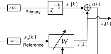
Without loss of generality, a two-channel TI-ADC is considered as shown in Fig. 7. Channel 0 is assumed to be reference branch for ANC algorithm. Thus, first and second channel outputs will be associated with reference and primary inputs respectively in terms of ANC technique. This structure is illustrated in Fig. 7:
W
1[ ]x k e k[ ]
[ ]
y k
0 ADC 1 A DC
0[ ]
x k
1
ˆ [ ]
x k
2 L
z
Fig. 7. Proposed compensated architecture for eliminating offset mismatch error in TI-ADC
Output of each channel includes two terms, one related to the input signal and the other one related to the offset, also it was mentioned previously that errors of ADC channels are independent. The proposed architecture is ANC block and so the error signal only includes the same independent terms of noisy and reference signals (channel 0 and channel 1). So as a simple result the output of filter would include the input signal term of channel 1 output and the offset term of output of channel 0. In other words, the adaptive filter output will converge to input-related term of other channel suppressing the offset. This means the filter output converges to X1[k] with offset equal to offset of reference branch. Then, the filter
output may be considered as recovered signal of second branch (see Fig. 7).
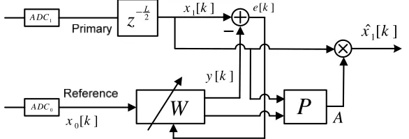
2. Correction of gain mismatch error: Considering a two-channel TI-ADC, the first channel is assumed as reference branch (Fig. 8). Thus, the first and second channel outputs will be associated with reference and primary inputs respectively in terms of ANC technique (see Fig. 6 and Fig. 8). Considering two-channel TI-ADC, it follows:
0 0 0
1 1 1
[ ] . [ ] [ ] . [ ]
x k G s k
x k G s k
(11)
where
s k
0[ ]
ands k
1[ ]
are associated to the input signals without gain error or desired signals of channel 0 and channel 1 respectively.W
1[ ]
x k e k[ ]
[ ] y k 0 ADC 1 A DC
0[ ]
x k
A
1
ˆ [ ]
x k
P
2 L
z
Fig. 8. Proposed architecture for eliminating gain mismatch error in TI-ADC
Filter output y[k] is an estimate of primary input. In other words, if error signal e[k] tends toward zero, y[k] will converge to the other channel's output as follows:
0 1
[ ] 0 [ ] [ ] [ ]
e k y k w x k x k (12)
where * denotes convolution operator. Considering relations (11) and (12), it may be shown that:
1. [ ]1 * 0. [ ]0
G s k w G s k (13)
And similarly, in frequency domain, it will be as follows:
1. 1f f. 0. 0f
G S W G S (14)
where S0f , S1f and Wf represent the Fourier transform of
s
0,s
1 andw
respectively. Since S0f and1f
S are associated with input signals at identical sampling rates without any gain error, so they have similar spectral magnitudes. This leads to:
2
1
0
| f |
G W
G
(15)
where |Wf | is the energy of filter through the input signal’s frequency range. To compute this parameter, ADC channel signal and the filter is needed. This parameter would be computed as follows:
1
1
| | F
f F
F
X
W W
X
(16)
where WF and X1F are the Fourier Transform of filter and x k1[ ] respectively and X1F stands for the
second norm of X1F. In the above formula, the term 1
1 F
F
X
X accounts for selecting the frequency range of
1[ ]
Processing block P (Fig. 8) first computes the energy of filter at input signal’s frequency range by (15) and then calculates its inverse as:
1 | f |
A W
(17)
Then, the gain coefficient of second channel after filtering (or compensation) would converge to the one related to the reference channel. The same as the previous section, because of the delay that the filter causes in the reference signal, a delay should be applied in primary signal and hence the output of architecture would be a delayed form of the original signal.
3. Proposed compensated TI-ADC architecture with correction of offset and gain mismatch errors:
In this section, an architecture for simultaneous elimination of offset and gain mismatch errors of TI-ADC is presented. For this purpose, the preceding architectures of Fig. 7 and Fig. 8 can be utilized in cascade. In fact, the offset mismatch error is compensated at the first step and then, the gain mismatch error would be eliminated at the second stage. The proposed architecture is illustrated in Fig. 9.
2
W
1[ ]
x k
0
ADC
1
A DC
0[ ]
x k
A
1
W
1
ˆ [ ] x k
P
2L
z
Fig. 9. Proposed architecture for eliminating both gain and offset mismatch errors in TI-ADC
In the previous sections, the proposed compensation technique for removing gain and offset mismatch errors has been described in the case of Two-Channel TI-ADC. In this section, the proposed compensation technique is extended for M-Channel TI-ADC. M-Channel compensation architecture is illustrated in Fig. 10:
0
ˆ
x
1
ˆ
x
1
ˆM
x
1
M
x
1
x
0
x
2
L
z
x t y k[ ]
In the proposed architecture, the first channel is chosen as reference channel. The number of ANC blocks with architecture of Fig. 9 are M-1. The first channel is considered the reference channel for all other channels and is used as the primary signal in the ANC blocks. As mentioned in previous sections, output of ANC block would be the reconstructed signal at the relative channel with a delay.
4. SIMULATION RESULTS
Simulations have been performed on a four-channel TI-ADC using branch ADCs, each channel having a resolution of 12 bits and a filter length of 256 coefficients, based on the proposed architecture for M-Channel TI-ADC(Fig. 10). SNR of the system’s output signal is used as a comparison criterion for evaluating the performance of the algorithm. Besides, the gain and offset at the output of architecture versus offset and gain of reference branch have been used to analyze the performance of proposed architecture.
In ANC technique, two important parameters that have effects on quality of method are Learning Factor and Filter Length L [18]. In this paper, filter length is regarded equivalent to 256 for simulations. To obtain the optimum value, a sweep has been run on the learning factor values and the optimum learning factor appears to approximately be:
1 L
(18)
Simulations are realized for three cases: A) eliminating offset mismatch error in the absence of gain mismatch, B) removing only gain mismatch and C) correcting the gain and offset mismatch errors simultaneously. These three cases are simulated based on proposed architecture at Fig. 10, in which the ANC block is replaced by proposed compensation block represented in Fig. 7, Fig. 8 and Fig. 9 respectively.
a) Performance in the presence of offset mismatch
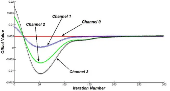
Simulations are performed on a four-channel TI-ADC in the presence of the offset mismatch between the channels. After about 200 iterations, the offset at output of each channel converges to the offset of reference branch (see Fig. 11):
Fig. 11. Offset value at the output of proposed architecture for eliminating offset mismatch
L 1 2
s 2
i 1
L 1 2
n 2
i 1
1
E Ideal [ k ] L
1
E Error [ k ] L
(19)where Ideal[k] and Error[k] represent noiseless input signal and error at kth time index respectively. Then, SNR can be obtained as follows:
10
Es S N R 20 L og
En
(20)
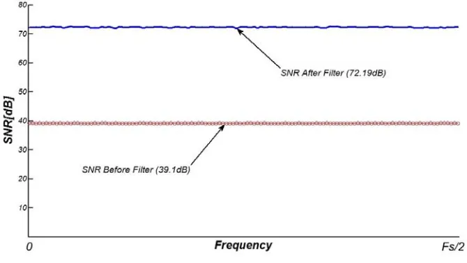
The SNR values have been compared versus input frequencies in Fig. 12. Proposed adaptive compensation technique has resulted in an evident improvement of 33.09dB compared to classical TI-ADC without compensation. Also, the improvement of offset compensation appears to be independent from the input frequency.
Fig. 12. SNR of TI-ADCs for proposed architecture (SNR After Filter) and classical uncompensated structure (SNR Before Filter) versus input frequency in presence of offset mismatch errors
b) Performance in the presence of gain mismatch
In this section, proposed architecture of Fig. 10 has been simulated considering the compensation structure proposed in Fig. 8 as ANC block of proposed architecture, and compared with the classical uncompensated TI-ADC. At this stage, it is assumed that only gain mismatch error exists. As mentioned in the previous section, SNR of output signal and gain of each channel are used to evaluate the performance of the proposed architecture. The Gain factors of channels converge to the gain of reference branch after about 1500 iterations (see Fig. 13).
Fig. 13. Gain of each channel versus iteration index in the proposed architecture for a four-channel TI-ADC
Fig. 14. SNR of TI-ADCS for proposed architecture (SNR After Filter) and classical uncompensated structure (SNR Before Filter) in the presence of gain mismatch errors
c) Performance in the presence of both offset and gain mismatch
In this section, the proposed architecture of Fig. 10 is simulated in the presence of both gain and offset mismatches. To compensate gain and offset mismatches simultaneously, the proposed architecture of Fig. 9 is used as ANC block in the proposed compensated architecture. SNR of output signal is used as evaluation parameter. The simulations have been realized for both proposed compensated and classical uncompensated architectures in a four-channel TI-ADC case. Fig. 15 exhibits the related SNR versus frequency of input signal. In the proposed adaptive structure, SNR is enhanced from 38dB to 71.2dB, i.e. an improvement of 33.2 dB has been obtained in SNR value. Results show that improved SNR is close to the ideal case (without gain and offset mismatch errors). In other words, gain and offset mismatch errors have been completely removed in compensated TI-ADC:
It is easily seen that the proposed technique leads to an evident improvement in output SNR. To evaluate the performance of the proposed method, SNR and Effective Number of Bits (ENOB) are compared in Table 1.
According to Table 1, offset and gain mismatch errors have been approximately eliminated in a four-channel ADC using the proposed compensation method.
Table 1. Performance of TI-ADCs with different architectures: Ideal TI-ADC without mismatch provides: SNR=73.6dB and ENOB=11.93 bits
Parameter SNR ENOB
TI-ADC Structure Uncompensated TI-ADC Proposed TI-ADC Uncompensated TI-ADC Proposed TI-ADC With offset
mismatch 39.1 72.19 6.2 11.7
With gain
mismatch 45.7 72 7.3 11.66
With gain and
offset mismatch 38 71.2 6.02 11.53
To better evaluate the performance of the proposed architecture, the power density of output signal in TI-ADC and proposed architecture is compared in Fig. 16. The peaks in Fs/2, Fs/2-Fin, Fs/4+Fin, Fs/4 and Fs/4-Fin are related to the gain and offset mismatch error in the four-channel TI-ADC. As shown in Fig. 16, the peaks related to gain and offset mismatch error are omitted in the proposed architecture:
-120 -100 -80 -60 -40 -20 0
Output of TI-ADC
Frequency PS D [dB ] -120 -100 -80 -60 -40 -20 0
Output of Proposed Architecture
PS D [dB ] Frequency Fin Fs/4+Fin Fs/2-Fin Fs/2 Fs/4-Fin Fs/4 Fin
Fig. 16. Spectrum of output signal for uncompensated TI-ADC (left) and proposed TI-ADC architecture (right). Noise caused by mismatch errors is removed at the proposed TI-ADC architecture
As mentioned in the introduction, the proposed method is independent of input signal. To evaluate the performance, an input signal of multiple sinusoids is applied. This input includes four frequencies. The performance of the proposed method is shown in Fig. 17:
-100 -50 0 Frequence PSD [d B ] -100 -50 0 Frequence PSD [d B ] -100 -50 0 Frequence PSD [d B ] Fs/2 Fs/2 Fs/2 0 0 0
The spectrum of original signal, uncompensated signal and compensated signals is shown in Fig. 17. Original signal’s spectrum includes four peaks related to the four frequencies of signal. There are some extra peaks in the spectrum of uncompensated TI-ADC output caused by gain and offset mismatch errors. The output signal of compensated architecture includes only the four peaks of the original input signal.
To compare and evaluate the performance of the proposed algorithm, the results of the proposed technique have been compared with other works in Table 2.
Table 2. Comparison between proposed Architecture and some other references
Algorithm
SNR
Resolutio
n Input signal Ideal Compensated Improveme
nt
[10] 61.98 56.8 - 10 Single sinusoid
[11] 85.7749 85.7311 41.9782 14 Single sinusoid
[14] - 66 30.9 11 Single sinusoid
Proposed 73.21 71.2 33.2 12 4 sinusoids
5. CONCLUSION
Errors originated from channel mismatches are a main bottleneck in realizing wide-band TI-ADCs with acceptable global output resolutions. In this paper, a new compensated architecture has been proposed for TI-ADC using an adaptive filter to eliminate gain and offset mismatches. It was shown that gain and offset mismatch errors can be efficiently eliminated in TI-ADC using proposed adaptive architecture without any a priori information about the input signal. Simulation results show that this technique is able to completely correct gain and offset mismatches in four-channel TI-ADC. Besides, the proposed compensation technique is digitally realized in the proposed TI-ADC without any need for extra analog circuitry. Then, requiring no extra hardware complexity, it can easily be implemented on IC level as an advantage. Applications of the proposed compensated TI-ADC can be used in most of the RF communication systems. However, it seems that efficiency of the proposed architecture in all applications of wide-band ADCs will not be as good as efficiency in RF communication systems and it is a disadvantage of the proposed architecture and also can be a point of future works.
REFERENCES
1. Asemani, D. & Oksman, J. (2007). A wide-band A/D converter for the software-defined radio system. IEEE ICSPC, Dubai, pp. 947-950.
2. Jondral, F. K. (2005). Software-defined radio: basics and evolution to cognitive radio. IEEE EURASIP, Vol. 3, pp. 275–283.
3. Vaithianathan, V., Raja, J. & Srinivasan, R. (2012). A low power, high gain, low noise amplifier with improved noise figure and input matching for ultra wide band applications. Iranian Journal of Science & Technology,
Transactions of Electrical Engineering, Vol. 36, No. E2, pp. 163-174.
4. Asemani, D. & Oksman, J. (2007). Time-division multiplexing architecture for hybrid filter bank A/D converters. IEEE MWSCAS, Canada, pp. 405–408.
5. Papoulis, A. (1977). Generalized sampling expansion. IEEE Trans. Circuits Syst., Vol. 24, No. 11, pp. 652–654. 6. Brown, J. L. (1981). Multi-channel sampling of low pass signals. IEEE Trans. Circuits. Systems, Vol. 28, No. 2,
7. Karamalis, P. D., Skentos, N. D. & G. A. (2006). Kanatas, adaptive antenna subarray formation for MIMO systems. IEEE Trans. Wireless Communications, Vol. 5, 11, pp. 2977–2982.
8. Black, W. C. & Hogges, A. A. (1980). Time interleaved converter arrays. IEEE J. Solid-State Circuits, Vol. 15, No. 6, pp. 1022–1029.
9. Petraglia, A. et al. (1991). QMF-based A/D converters: Overview and new results. Int. Conf. A/D and D/A Conversion, pp. 112-117.
10. Seo, M. & Rodwell, M. J. W. (2005). Comprehensive digital correction of mismatch errors for a 400-Msamples/s 80-dB SFDR time-interleaved analog-to-digital converter. IEEE Trans. Microwave Theory and
Techniques Society, Vol. 53, No. 3, pp. 1072–1082.
11. Jamal, S. M., Fu, D., Hurst, P. J. & Lewis, S. H. (2002). A 10-b 120-Msample/s time-interleaved analog-to-digital converter with analog-to-digital background calibration. IEEE Solid-State Circuits Society, Vol. 37, No. 12, pp. 1618-1628.
12. Xu, G. X., Yan, B., Li, Q. & Li. G. J. (2010). Adaptive calibration of gain and offset errors for time-interleaved
ADCs. IEEE Asia Pacific conference on postgraduate research in microelectronics and electronics, China, pp. 77-81.
13. Seo, M., Rodwell J. W. & Madhow, U. (2006). A low computation adaptive blind mismatch correction for time-interleaved ADCs. IEEE MWSCAS, Puerto Rico, pp. 292-296.
14. Seo, M. & Rodwell, J. W. (2007). Generalized blind mismatch correction for a two-channel time-interleaved ADC: Analytic approach, ISCAS 2007, New Orleans, LA, pp. 109-112.
15. Vogel, C., Saleem, S. & Mendel, S. (2008). Adaptive blind compensation of gain and timing mismatches in M-channel time-interleaved ADCs. ICECS, St. Julien's, Italy, pp. 49–52.
16. Asami, K. (2005). Technique to improve the performance of time-interleaved A-D converters. IEEE International Conference on Test, pp. 851–857.
17. Kurosawa, N., Kobayashi, H., Maruyama, K., Sugawara, H. & Kobayashi, K. (2001). Explicit analysis of channel mismatch effects in time-interleaved ADC systems. IEEE Transactions. Fundamental Theory and
Applications, Vol. 48, No. 3, pp. 261-271.
18. Widrow, B., Glover, J. R., McCool, J. M., Kaunitz, J., Williams, C. S., Hearn, R. H., Zeidler, J. R., Dong, E. & Goodlin, R. C. et al. (1975). Adaptive noise cancelling: Principles and applications. Proceeding of the IEEE, Vol. 63, No. 12, pp. 1692-1716.