RTL Level and Self-Test Approach Based
Arithmetic BIST
Shaik Anjumara1, P. Bala Murali Krishna2 1
PG student, Department of ECE, Sri Mittapalli institute of Technology for Women, Guntur, Andhra Pradesh, India
2
Professor , Department of ECE, Sri Mittapalli institute of Technology for Women, Guntur, Andhra Pradesh, India
Abstract---In this paper an accumulator-based 3-weight test pattern generation scheme is presented. First, it does not impose any requirements about the design of the adder i.e., it can be implemented using any adder design and then it does not require any modification of the adder; and hence it does not affect the operating speed of the adder. Furthermore, the proposed scheme compares favourably to the scheme proposed in terms of the required hardware overhead. The weighted random test pattern generation represents a significant departure from classical methods of generating test sequences for complex large scale integration packages. The virtue of this technique is its simplicity and the fact that test-generation time is virtually independent of gates in the logic package to be tested. This technique can be used both in a conventional tester and in a tester where the weighted random test pattern generation is implemented in hardware. By this proposed method the patterns are generated with reduced delay.
Key Words: 3-Weight Test Pattern Generation, Hardware Overhead, Random Test Pattern Generation.
I. INTRODUCTION
BIST is a design-for-testability technique that places the testing functions physically with the circuit under test (CUT). The basic BIST architecture requires the addition of three hardware blocks to a digital circuit: a test pattern generator, a response analyzer, and a test controller. The test pattern generator generates the test patterns for the CUT[1]. Examples of pattern generators are ROM with stored patterns, a counter, and a linear feedback shift register (LFSR) [2]. A typical response analyzer is a comparator with stored responses or an LFSR used as a signature analyzer. It compacts and analyzes the test responses to determine correctness of the CUT. A test control block is necessary to activate the test and analyze the responses. However, in general, several test-related functions can be executed through a test controller circuit. A new weighted random pattern design for testability is described where the shift register latches distributed throughout the chip are modified so that they can generate biased pseudo-random patterns upon demand. A two-bit code is transmitted to each weighted random pattern shift register latches to determine its specific weight. The weighted random pattern test is then divided into groups, where each group is activated with a different set of weights [7]. The weights are dynamically adjusted during the course of the test to "go after" the remaining untested faults.
An accumulator-based 3-weight test pattern generation scheme is presented; the proposed scheme generates set of patterns with weights 0, 0.5, and 1 [10], [15]. Since accumulators are commonly found in current VLSI chips, this scheme can be efficiently utilized to drive down the hardware of built in self test pattern generation, as well. Comparisons with previously presented schemes indicate that the proposed scheme compares favourably with respect to the required hardware.
II. WEIGHT GENERATING COMBINATIONAL CIRCUIT
A digital system is tested and diagnosed during its lifetime on numerous occasions. Such a test and diagnosis should be quick and have very high fault coverage. One way to ensure this is to specify such a testing to as one of the system functions, so now it is called Built In Self Test (BIST) [6]. With properly designed BIST, the cost of added test hardware will be more than balanced by the benefits in terms of reliability and reduced maintenance cost.
A. Weighted Generation Of BIST
each fault simulation at a place on the chip (like ROM). An n input circuit would then require 2^n combinations which can be very tiresome on the system with respect to the space and the time. Also, more the number of transitions, the power consumed will be more.
1) BIST Techniques: The BIST techniques are classified based on the operational condition of the circuit under test (CUT):On-Line BIST, Off-(CUT):On-Line BIST. In On-line BIST the testing occurs during normal functional operating conditions. Here there is no test mode, and real-time error detection. There are two types of on-line BIST techniques one is Concurrent and other is Non-Concurrent. The concurrent occurs simultaneously with normal functional operation where it is realized by using coding techniques. While the non-concurrent carried out while in idle state, interruptible in any state realized by executing diagnostic software/firmware routines. Off-line BIST deals with testing a system when it is not carrying out its normal functions i.e.; test mode, Non-Real-Time error detection. It can be tested by using on-board TPG + Output Response Analyzer (ORA) or Micro diagnostic routines. There are two types of off-line BIST techniques Structural off-line BIST and Functional off-line BIST. The execution of structural off-line BIST based on the structure of the CUT (Explicit fault model – LFSR). The Functional off-line BIST is running based on functional description of CUT (Functional fault model - diagnostic software).
2) Test Pattern Generation Techniques: There are 3 types of test pattern generation techniques:
Exhaustive testing, Pseudo exhaustive testing, Pseudo random testing. In Exhaustive testing Applying all 2**n input combinations, generated by binary counters or complete LFSR. In Pseudo exhaustive testing the circuit is segmented and each segment is tested exhaustively i.e., Less no. of tests required. In Pseudo random [4] testing it reduces the test length but sacrifices the fault coverage and it is difficult to determine the required test length and fault coverage.
3) Test Response compression techniques: The below are the test response compression techniques:Response Compression, Signature, Alias, Compression Procedure. In Response compression there is a process to form a “signature” from complete output responses. TheSignature compressed form of saved test results. The Alias error outs the output when faulty & fault-free signature are same. In Compression procedure the composition of test vector applying, results storing and comparison of the faulty & fault free signatures.and the compression of simple hardware implementation and small performance degradation - no effect on normal circuit behaviour (delay, execution time). The high degree of compression - signature lengths to be a logarithmic factor of responses lengths and small aliasing errors.
III. ACCUMULATOR BASED 3-WEIGHT PATTERN GENERATION
Generally, the accumulator-based compaction technique uses an accumulator to generate a composite fault signature for a circuit under test. The error coverage for this method has been previously analyzed. We describe an alternative technique for calculating the error coverage of accumulator-based compaction using the asymmetric error model. This technique relies on the central limit theorem of statistics and can be applied to other count-based compaction schemes [9]. The data paths of most contemporary general and special purpose processors include registers, adders and other arithmetic circuits. If these circuits are also used for built-in self-test, the extra area required for embedding testing structures can be cut down efficiently. Several schemes based on accumulators, subtractions, multipliers and shift registers have been proposed and analyzed in the past for parallel test response compaction, whereas some efforts have also been devoted in the bit-serial response compaction case.
The utilization of accumulators for time compaction of the responses in built-in self test environments has been studied by various researchers. One of the well-known problems of time compactors is aliasing [12], i.e. the event that a series of responses containing errors result in a signature equal to that of an error-free response sequence. In this paper we propose a scheme to reduce aliasing in accumulator based compaction environments. With the proposed scheme, the aliasing probability tends to zero, as the number of the patterns of the test set increases.
We use a pseudo random generator made using Linear Feedback Shift Register (LFSR). These patterns generated using LFSR have all the desirable properties of random numbers, but are algorithmically generated by the hardware pattern generator and are therefore repeatable.
random pattern generation‟ in order to obtain an acceptable fault percentage. This desire to achieve higher fault coverage with shorter test lengths and therefore shorter test times led to the invention of the weighted pseudo random pattern generator.
[image:4.612.230.377.148.221.2]The implementation of the weighted-pattern generation scheme is based on the full adder truth table, presented in Table II. From Table II we can found that Cout = Cin.
Table I Test Set for the c17 Benchmark
Test Vector Inputs A[4:0] T1
T2 T3 T4
00101 01010 10010 11111
Table II Truth Table for Full Adder
A. Accumulator Cell
The main object of the weighted pattern generation is an accumulator cell [3]. To implement the accumulator in the proposed weighted pattern generation scheme is based on presented in Fig1.
Fig.1: Accumulator cell
Which consists of a Full Adder (FA) cell and a D-type flip-flop with asynchronous set and reset inputs whose output is also driven to one of the full adder inputs. In the above figure, we assume that the set and reset are active high signals and at the same time the set and reset are used to without loss of generality. And at the time, the respective cell of another register B[i] is also occurred. For this accumulator cell, one out of three configurations can be utilized, as shown in Fig: 2.
In Fig: 2 we present the configuration that drives the CUT inputs. When A[i] =1 is required, So the set[i]=1 and reset[i]=0 and hence A[i]=1 and B[i]=0. Then the output is equal to 1, and Cin is equal to Cout. i.e., the Cin is transferred to the Cout. And similarly, When A[i] =0 is required, So the set[i]=0 and reset[i]=1 and hence A[i]=0 and B[i]=1. Then the
[image:4.612.216.354.401.574.2]Fig.2: Configurations of the accumulator cell of Fig.1.
When A[i] = “-” is required, so the set[i] =0 and reset[i]=0. The D input of the flip-flop of register B is driven by either 1 or 0, depending on the value that will be added to the accumulator inputs in order to generate satisfactorily random patterns to the inputs of the CUT.
B. Linear Feedback Shift Registers
The LFSR are the basic building blocks of the pseudo random test pattern generators. In unbiased pseudo random testing, the outputs from the LFSR is fed directly to the CUT and thus the no. of LFSR stages required is equal to the number of inputs to the CUT. For a weighted pseudo random testing we however require much more LFSR stages than the inputs to the CUT. This is so because each weighted bit usually requires more than one equi-probable bit coming in from an LFSR stage for the generation of its weighted bit. Now we assume that for both the unbiased and the weighted case we have the total number of LFSR shift registers required for each of the CUTs.
C. Pattern Generation
In the last section we see how, depending upon the no. of inputs of the CUT and the associated probabilities we can make an LFSR [1] configuration for both, the unbiased and the weighted pseudo random testing part. We do this by writing a Verilog file with the entire configuration written in it. After that we run the Verilog simulator and get the raw patterns in a file. This reads the patterns generated from an LFSR working for weighted pseudo random testing.
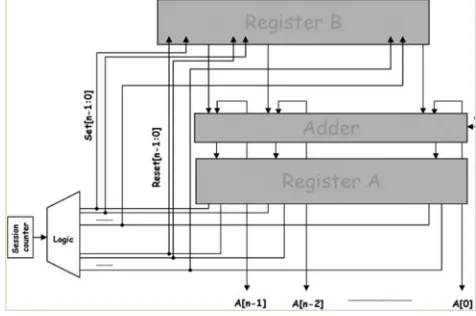
[image:5.612.182.420.547.705.2]The general configuration of the proposed scheme is presented. The Logic module provides the Set [n-1:0] and Reset [n-1:0] signals that drive the S and R inputs of the Register A and Register B inputs. Note that the signals that drive the S inputs of the flip-flops of Register A, also drive the R inputs of the flip-flops of Register B and vice versa.
All schemes require the application of the session counter, required to alter among the different weight sessions. The number of test patterns applied and the proposed scheme is the same, since the test application algorithms that have been invented and applied, Methods to generate weighted pseudo-random patterns for combinational circuits that can be extended to sequential circuits this method is based on the use of three weights, 0, 0.5 and 1. A weight assignment associates one of these weights with every primary input of the circuit. A preselected number of patterns N is applied under every weight assignment [10]. A weight of 0.5 assigned to an input i by a weight assignment w implies that pseudo-random patterns are applied to input i while N test patterns are applied to the circuit; a weight of 0 assigned to input i implies that input i is held at 0 constantly for the N test patterns and a weight of 1 assigned to input i implies that input i is held at 1 constantly for the N test patterns. The weight assignments are based on a deterministic test set. Each weight assignment is obtained by intersecting a subset of deterministic test patterns. The intersection of identical values, 0 or 1, yields a weight of 0 or 1, respectively.
The intersection of different values yields an unspecified value (x), which is translated into a weight of 0.5[15]. The intersection of test sub sequences yielded weight assignments that were used in a similar way to the ones for combinational circuits. However, for sequential circuits, the intersection of a subset of test subsequence of length M results in M weight assignments that have to be used consecutively, and changed at every time unit. The need to change the weight assignment at every time unit is undesirable.
IV. RESULTS ANALYSIS
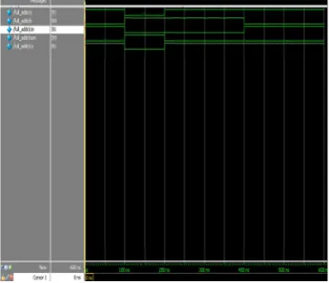
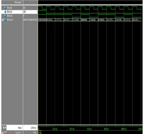
[image:6.612.215.399.332.506.2]The proposed system is implemented by using Xilinx Software and the simulation waveforms of each module are shown below.
Fig. 4: D Flip Flop
A. D-Flip flop
D-Flip flop is the basic flip flop of counter used in this project. When clock signal goes logically high the output gets the value which applied to the input.
[image:6.612.235.416.549.705.2]B. Full Adder
[image:7.612.184.426.115.339.2]Full adderis an adder in order to design accumulator cell to generate test vectors for the scan operation of the signature registers.
Fig. 6: Accumulator Cell
C. Accumulator Cell
When Set[i]=1 and Reset[i]=0 and hence A[i]=1 and B[i]=1.Then, output is equal to 1, and Cin is transferred to Cout. The logic
module of Accumulator cell provides Set[n-1:0] and Reset[n-1:0] signals that drive the S and R inputs of the Register A and Register B. Note that the signals that drive the S inputs of the flip flops of Register A, also drive the R inputs of Register B and vice versa.
Fig. 7: Linear Feedback Shift Register
D. Linear Feed Back Shift Register
[image:7.612.184.427.410.638.2]Fig. 8: Session Counter
E. Session Counter
All the schemes require the application of the session counter, required to alter among the different weight sessions.
Fig .9: Top Module
F. Top Module
As per the session counter count the Cin from the Registers transferred as the Cout to generate test vectors for weight patterns.
G. Comparisons
[image:8.612.179.432.345.612.2]TABLE IIIComparison with [11]
[image:9.612.40.429.236.400.2]In table III, we shall compare the proposed scheme with the accumulator-based 3-weight generation scheme that has been proposed in [11]. In Section IV-B, we shall compare the proposed scheme with the 3-weight scan schemes that have been proposed in [5] and [8].
TABLE IV: Comparisons with the Scan Scheme Proposed in [5] and [8]
In the 3-weight pattern generation scheme proposed by Pomeranz and Reddy in [5] the scan chain is driven by the output of a linear feed-back shift register (LFSR). Serial fixing scheme is shown tobe more costly [8]; therefore we shall concentrate our comparisons to the parallel fixing BIST scheme.
H. Device Utilization Summary
The below table v is the device utilization summary in the synthesis report after completion of simulation process.
TABLE V: Design Utilization Summary
V. CONCLUSION
We have presented an accumulator-based 3-weight (0, 0.5, 1) test-per-clock generation scheme, which can be utilized to efficiently generate weighted patterns without altering the structure of the adder. Comparisons with a previously existing accumulator-based 3-weight pattern generation technique and it indicates that the hardware overhead of the proposed scheme is lower, while at the same time no redesign of the accumulator is imposed, thus resulting in reduction in test application time. Comparisons with existing scan based schemes show that the proposed schemes results in lower hardware overhead. Finally, comparisons with the accumulator- based scheme proposed and reveal that the proposed scheme results in significant decrease in hardware overhead and the amount of time it required to generate the results is very low.
[image:9.612.43.444.489.616.2]REFERENCES
[1] P. Bardell, W. McAnney, and J. Savir, Built-In Test For VLSI: Pseudorandom Techniques. New York: Wiley, 1987
[2] P. Hortensius, R. McLeod, W. Pries, M. Miller, and H. Card, “Cellular automata-based pseudorandom generators for built-in self test,” IEEE Trans. Comput.-Aided Des. Integr. Circuits Syst., vol. 8, no. 8, pp. 842–859, Aug. 1989.
[3] A. Stroele, “A self test approach using accumulators as test pattern generators,” in Proc. Int. Symp. Circuits Syst., 1995, pp. 2120–2123. [4] H. J. Wunderlich, “Multiple distributions for biased random test patterns,” in Proc. IEEE Int. Test Conf., 1988, pp. 236–244.
[5] I. Pomeranz and S. M. Reddy, “3 weight pseudo-random test generation based on a deterministic test set for combinational and sequential circuits,” IEEE Trans. Comput.-Aided Des. Integr. Circuits Syst., vol.12, no. 7, pp. 1050–1058, Jul. 1993.
[6] K. Radecka, J. Rajski, and J. Tyszer, “Arithmetic built-in self-test for DSP cores,” IEEE Trans. Comput.-Aided Des. Integr. Circuits Syst., vol. 16, no. 11, pp. 1358–1369, Nov. 1997.
[7] J. Rajski and J. Tyszer, Arithmetic Built-In Self Test For Embedded Systems. Upper Saddle River, NJ: Prentice Hall PTR, 1998. [8] S. Wang, “Low hardware overhead scan based 3-weight weighted random BIST,” in Proc. IEEE Int. Test Conf., 2001, pp. 868–877.
[9] S. Zhang, S. C. Seth, and B. B. Bhattacharya, “Efficient test compaction for pseudo-random testing,” in Proc. 14th Asian Test Symp., 2005, pp. 337–342. [10] J. Savir, “Distributed generation of weighted random patterns,” IEEE Trans. Comput., vol. 48, no. 12, pp. 1364– 1368, Dec. 1999.
[11] I. Voyiatzis, D. Gizopoulos, and A. Paschalis, “Accumulator-based weighted pattern generation,” presented at the IEEE Int. Line Test Symp., Saint Raphael, French Riviera, France, Jul. 2005.
[12] I. Voyiatzis, “An accumulator—based compaction scheme with re-duced aliasing for on-line BIST of rams,” IEEE Trans. Very LargeScale Integr. (VLSI) Syst., vol. 16, no. 9, pp. 1248–1251, Sep. 2008.
[13] J. Rajski and J. Tyszer, Arithmetic Built-In Self Test For Embedded Systems. Upper Saddle River, NJ: Prentice Hall PTR, 1998. [14] S. Wang, “Low hardware overhead scan based 3-weight weighted random BIST,” in Proc. IEEE Int.
[15] F. Brglez, C. Gloster, and G. Kedem, “Hardware-based weighted random pattern generation for boundary scan,” in Proc. IEEE Int. TestConf. (ITC), 1989, pp. 264–274.
![Table II we can found that Cout = Cin. Table I Test Set for the c17 Benchmark Test Vector Inputs A[4:0]](https://thumb-us.123doks.com/thumbv2/123dok_us/8582627.861392/4.612.216.354.401.574/table-cout-table-test-benchmark-test-vector-inputs.webp)

![TABLE IIIComparison with [11]](https://thumb-us.123doks.com/thumbv2/123dok_us/8582627.861392/9.612.43.444.489.616/table-iiicomparison-with.webp)
