International Journal of Emerging Technology and Advanced Engineering
Website: www.ijetae.com (ISSN 2250-2459, ISO 9001:2008 Certified Journal, Volume 6, Issue 1, January 2016)
145
Design of Switched Capacitor Amplifier for sampled
output-using 180nm CMOS Technology
Soumen Pal
1, Pinkey Ghosh
2, Pranab Hazra
31,2,3
Narula Institute of Technolgy, 81 Nilgunj Road, Agarpara, Kolkata-700109, India
Abstract— Analog sampled data techniques were used to replace the resistor, resulting in the circuits consisting of only MOSFET switches, capacitors and op-amps. These circuits are called switched capacitor circuits and have become a popular method of implementing analog signal-processing circuit in standard technologies. CMOS op-amp are integral part in various analog and mixed signal circuits and system. The two stage op-amp is widely used for its simple structure and robustness. The aim of the design methodology in this paper is to produce amplified sampled signal from analog input using 180nm CMOS technology for 1.8v supply voltage . The method handles a very wide variety of specifications and constraints. In this paper a low power two stage op-amp has been designed and its application as switched capacitor amplifier has been presented. The simulation result confirm the correctness of design procedure and parameter selection.
Keywords— Switched capacitor, CMOS, Sampled signal, op-amp, trans-resistive.
I. INTRODUCTION
An operational amplifier (op-amp) is an electronic voltage amplifier with very high differential gain. It has differential input and usually a single-ended output. Operational amplifiers are inseparably used in analog computers, where they were used to do mathematical operations in many linear, non-linear and frequency-dependent circuits. Functionality of a circuit using an op-amp are set by external components with little dependence on temperature changes or manufacturing variations in the op-amp itself, which makes op-amps a popular building block for electronic circuit design. Op-amps are the most widely used electronic device today, being used in a vast array of consumer, industrial, and scientific devices.
Operational amplifiers (Op-Amps) are basic building blocks of a wide range of analog and mixed signal systems. Basically, Op-Amps are voltage amplifiers being used to achieve high gain by applying differential input. The gain is typically between 50 to 60 decibels. This means that even very small voltage difference around tens of mili-volts between the input terminals drives the output voltage to the supply voltage. As new generations of CMOS technology tend to have shorter transistor channel length and scaled down supply voltage, the design of Op-Amps stays a challenge for designers.
The operational amplifier is a versatile device that can be used to amplify dc as well as ac input signals and was
originally designed for performing mathematical
operations. It was found that the application of negative feedback around a high gain amplifier would produce a circuit with a precise gain characteristic that depended only on the feedback used. By the proper selection of feedback components, an operational amplifier could be used to add, subtract , integrate, and differentiate. The designing of Op-Amps puts new challenges in low power applications with reduced channel length devices. On the other hand advancements which have appeared recently through new techniques and technologies, give us multiple alternatives in implementations of CMOS circuits.
In two stage CMOS Op–Amps because of two dominant poles the phase margin could easily reach to less than the amount which is just enough for stable operation. This serious problem should be taken care of by designers, otherwise there is a possibility that the Op-amp output will oscillate and instead of an amplifier it will become an oscillator. In some applications the gain and or the output swings provided by cascade op-amps are not adequate. In such cases, we resort to "two stage" Op-Amps, with the first stage providing a high gain and the second stage providing large output swing. In contrast to cascade Op-Amps, a two-stage configuration isolates the gain and swing requirements as well to provide more gain and more output swing[1]. In designing an op-amp, numerous electrical characteristics, such as supply voltages, DC gain, load capacitance, unity gain frequency, phase margin, slew rate, input common mode range, output swing, all have to be taken into consideration. Op-amps are designed to be operated with negative feedback connection as frequency compensation is necessary for closed loop stability. So the designing an op-amp that satisfy all the electrical specification requires a good compensation strategy and design technique [1].
International Journal of Emerging Technology and Advanced Engineering
Website: www.ijetae.com (ISSN 2250-2459, ISO 9001:2008 Certified Journal, Volume 6, Issue 1, January 2016)
146
But in VLSI circuit realization of high value active resistor using MOS transistors requires large area. So in VLSI circuit resistors are realize using the combination of switch and capacitor which can be a better alternative in concern with area requirement. In addition to that switched capacitor circuit is very much compatible with CMOS technology. A switched capacitor is an electronic circuit element used for discrete time signal processing. It works by moving charges into and out of capacitors when switches are opened and closed. Usually, non-overlapping signals are used to control the switches, so that not all switches are closed simultaneously.
II. SWITCH CAPACITOR CIRCUIT
Analog sampled data techniques were used to replace the resistor, resulting in the circuits consisting of only MOSFET switches, capacitors and op-amps. These circuits are called switched capacitor circuits and have become a popular method of implementing analog signal-processing circuit in standard technologies. One of the important reasons for the success switched capacitor circuits is that the accuracy of the signal processing function is proportional to the accuracy of the capacitor ratios. A switch-capacitor (―SC‖) amplifier includes a two-stage operational amplifier (―OP-AMP‖), an input SC network, and a feedback SC network. The two-stage OP-AMP includes a first OP-AMP stage having an output coupled to an input of a second OP-AMP stage. The input SC network is coupled to an input of the first OP-AMP stage. Feedback SC network is configured to selectively couple the output of the first OP-AMP stage to the input of the first OP-AMP stage during a first phase of operation of the sc amplifier and to couple an output of the second OP-AMP stage to the input of the first OP-AMP stage during a second phase of operation of the SC amplifier.
Switched capacitor circuits have reached maturity in CMOS technology. The switched capacitor circuit concept was a pivotal step in the implementation of analog signal processing circuits in CMOS technology. The accuracy of the signal processing is proportional to capacitor ratios.
Switched capacitor circuits have been developed for
Amplification, Filtering, Comparing, Analog-digital
conversion.
Properties of Switched Capacitor Circuit
The entire Popular due to accurate frequency
response, good linearity and dynamic range Easily analysed with z-transform
Typically require aliasing and smoothing filters
Accuracy is obtained since filter coefficients are determined from capacitance ratios, and relative matching is good in CMOS
The overall frequency response remains a function of
the clock, and the frequency may be set very precisely through the use of a crystal oscillator
SC-techniques may be used to realize other signal processing blocks like for example gain stages, voltage controlled oscillators and modulator
Advantages of Switched Capacitor Circuit
Compatibility with CMOS technology.
Good accuracy of time constants.
Good voltage linearity.
Good temperature characteristics.
Disadvantages of Switched Capacitor Circuit
Clock feed through.
Requirement of non overlapping clock.
Signal frequency must be less than clock
frequency.
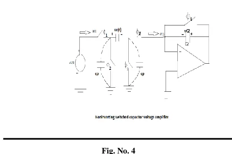
III. POSITIVE AND NEGATIVE TRANSRESISTIVE SWITCHED CAPACITOR CIRCUIT
Analog Transresistive circuits are two-port networks where the voltage across one port controls the current flowing between the ports. Typically, one of the ports is at zero potential (virtual ground). These are Negative transresistive circuit, Positive transresistive circuit[8]
.
Fig. No. 1
International Journal of Emerging Technology and Advanced Engineering
Website: www.ijetae.com (ISSN 2250-2459, ISO 9001:2008 Certified Journal, Volume 6, Issue 1, January 2016)
147
[image:3.612.50.286.244.592.2]These results are only valid when fc >> f. Where fc is clock frequency and f is signal frequency. These circuits are insensitive to the parasitic capacitances shown as dotted capacitors.
Fig. No. 2
When the switches in are closed, cp are shorted out
and cannot be charged. During the phase, the parasitic
capacitors are either connected in parallel with or
shorted out during the next phase period .
Fig. No. 3
During the Φ2 phase, the circuit is equivalent to the inverting charge amplifier with a negative input of applied as a consequence, the output voltage can be written as
(n-1/2)T =
We note that during the Φ1 phase, both C1 and C2 are discharged. Consequently, there is no charge transferred between the Φ1 and Φ2 phase periods. During the Φ2 phase period, it is simply the inverting charge amplifier. The output voltage during the phase period is written as
We note that the output voltage has no delay with respect to the input voltage. The z domain equivalent expression is
[image:3.612.328.555.296.447.2](z)
Fig. No. 4
We begin with the Φ1 phase during the time from t = (n-1)T to t = (n-1/2)T. the voltages across each capacitor can be written as
(n-1)T = (n-1)T and (n-1)T = (n-1)T =
International Journal of Emerging Technology and Advanced Engineering
Website: www.ijetae.com (ISSN 2250-2459, ISO 9001:2008 Certified Journal, Volume 6, Issue 1, January 2016)
148
RESULT ANALYSIS
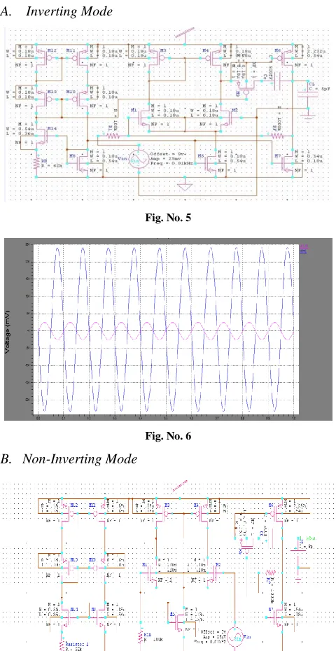
IV. CONTINUOUS TIME AMPLIFIER
[image:4.612.323.578.113.264.2]A. Inverting Mode
Fig. No. 5
Fig. No. 6
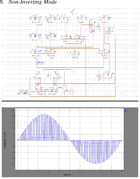
B. Non-Inverting Mode
Fig. No. 7
Out-put waveform of non-inverting amplifier
Fig. No. 8
V. SWITCHED CAPACITOR AMPLIFIER
[image:4.612.48.288.172.637.2]A. Inverting Mode
Fig. No. 9
Out-put waveform of inverting amplifier
[image:4.612.326.561.314.643.2]International Journal of Emerging Technology and Advanced Engineering
Website: www.ijetae.com (ISSN 2250-2459, ISO 9001:2008 Certified Journal, Volume 6, Issue 1, January 2016)
149 B. Non-Inverting Mode
[image:5.612.45.566.130.646.2]Out-put waveform of non-inverting amplifier
Fig. No. 11
C. DC Response for Inverting Mode
Fig. No. 12
[image:5.612.50.286.138.439.2]D. DC Response for Non-Inverting Mode
Fig. No. 13
E. Transient Response for Inverting Mode
Fig. No. 14
TABLEI
DESIGN PARAMETERS OF SWITCHED CAPACITOR AMPLIFIER CIRCUIT USING OP-AMP.
parameter value unit
Cc 0 .5 pF
RB 62 kΩ
(W/L)1,2 0.18/0.18 µm/ µm
(W/L)3,4 0.18/0.18 µm/ µm
(W/L)5,8 0.18/0.54 µm/ µm
(W/L)6 2.232/0.54 µm/ µm
(W/L)7 0.54/0.18 µm/ µm
(W/L)9 0.18/0.18 µm/ µm
(W/L)10-13 0.18/0.18 µm/ µm
(W/L)14 0.54/0.36 µm/ µm
[image:5.612.322.573.146.393.2]International Journal of Emerging Technology and Advanced Engineering
Website: www.ijetae.com (ISSN 2250-2459, ISO 9001:2008 Certified Journal, Volume 6, Issue 1, January 2016)
150
VI. CONCLUSION
Here the design procedure for two stage low power CMOS op-amp has been presented. The simulation result confirms that the design procedure is suitable for low power CMOS op-amp design. I have also used the op-amp to realize the continuous time amplifier and switched capacitor amplifier for proper clock frequency input signal consideration. The result for switched capacitor non-inverting and non-inverting amplifier shows the amplification of continuous input signal in the sampled signal. This sampled signal is readily available for any sampled data systems. The simulated output of switched capacitor amplifier represents the correctness of parameter selections. The
results are compared with respect to standard
characteristics of the op-amp with the help of graph and table. Simulation result agree with theoretical prediction. Design has been carried out in TANNER tools ver. 13.
REFERENCES
[1] Jirayuth Mahattanakul,Member, IEEE, and Jamorn Chutichatuporn. ―Design procedure for Two stage CMOS op-amp with Flexible Noise power Balancing Scheme‖, Vol.52,no-8,August 2005. [2] B. Razavi, Design of Analog CMOS Integrated Circuits.
McGraw-Hill, 2002.
[3] J. Mahattanakul, ―Design procedure for two stage CMOS operational amplifier employing current buffer‖, IEEE trans. Circuits sys. II, Express Briefs, vol 52, no.11 nov 2005.International Journal of VLSI design & Communication Systems (VLSICS) Vol.2, No.1, March 2011.
[4] P.E. Allen and D.R. Holberg, CMOS Analog Circuit Design. Oxford University Press, 2002.
[5] Leonard Forbes, Harish Gopalakrishnan, and WeetitWanalertlak,―Simulation and analysis of noise in switched capacitor amplifier circuits‖, Microelectronics and Electron Devices, 2005. WMED '05. 2005 IEEE Workshop