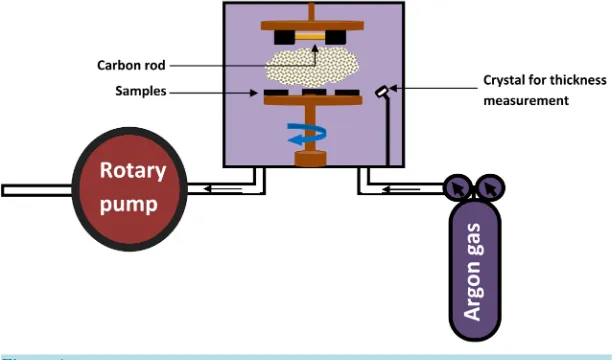
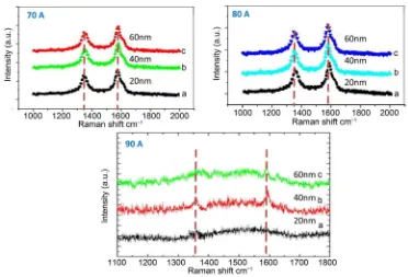
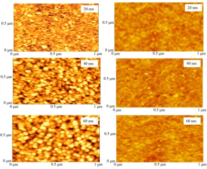
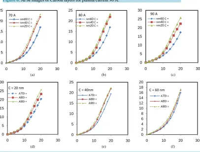
The Role of Sputtering Current on the Optical and Electrical Properties of Si C Junction
Full text
Figure
Related documents
The study was conducted using the survey model because its aim was to determine the TPACK of pre-service teachers in the departments of primary school elementary school teaching
A perceived way out of the administrative challenge was to transform university knowledge production in order to create jobs, ensure equitable income distribution, improve
The paper is discussed for various techniques for sensor localization and various interpolation methods for variety of prediction methods used by various applications
An unusually high percentage of these occurred in the left eyebrow which appears to be the most frequent location for dermoid cysts in children.. Dermoid cysts are a very common
Standardization of herbal raw drugs include passport data of raw plant drugs, botanical authentification, microscopic & molecular examination, identification of
RT-qPCR analysis demon- strated that gene expression of MMP3 and MMP9 was increased following IL-1 β stimulation ( p < 0.001, Fig. 1a ), and the induction was especially
The total coliform count from this study range between 25cfu/100ml in Joju and too numerous to count (TNTC) in Oju-Ore, Sango, Okede and Ijamido HH water samples as
As the results showed students and teachers in the three ESP contexts where content teachers, language teachers and professional ESP teachers of Language Departments teach ESP,
