Design Analysis of a Hexaband Slot Loaded Microstrip
Patch Antenna using ANN
Jatinder Pal Singh
Assistant Professor Dept. ECE, CTIEMT, ShahpurJalandhar, India
Amandeep Singh
Assistant Professor & Head Dept. ECE, CTIEMT, ShahpurJalandhar, India
Nancy Gupta
Assistant Professor Dept. ECE, CTIEMT, ShahpurJalandhar, India
ABSTRACT
The designing of an antenna is a critical area for the present wireless communication system. It is important to maintain an agreement amongst gain, bandwidth, return loss and VSWR characteristics of antenna. In this paper an exclusive design concept for the circular patch antenna is introduced. Initially a circular microstrip patch antenna is designed and the performance of this new design is enhanced after applying different types of slotted perturbations in one half of antenna. The antenna performance is transformed from single band to multiband by employing ‘Y’ shape slotted structures. The proposed antenna represents quad band behavior at resonant frequencies 2.44 GHz, 6.48 GHz, 7 GHz and 8.25 GHz with a good value of return loss of -12.29 dB, -16.48 dB, -15 dB and -27.81 dB respectively. This design also represents VSWR between the specified range of 1 to 2 for the said resonant frequencies with an acceptable value of gain in dB. The antenna is designed and simulated with FEM based electromagnetic field solver. The proposed antenna design is suitable for WLAN, Radio astronomy, Passive sensors and Point to Point defense system wireless applications. The proposed antenna is analyzed for proper coaxial feed location using radial basis function neural networks. The results obtained using RBF neural networks are in a good agreement to the simulation results obtained using electromagnetic solver. The feed location provided by the RBF neural networks results in six band behavior.
Keywords
Hexaband, Patch antenna, Wireless applications, ‘Y’ shape
1.
INTRODUCTION
In recent years the requirement for wireless communication systems has increased rapidly demanding quality of service, protection of information and increased data rate for the wireless local area networks (WLANs). The main aim of advance wireless communication system is high speed networking service for different media communication. Microstrip patch antennas offer numerous advantages such as low cost, light weight, low profile, ease of fabrication and conformity [1-2]. Instead of these advantages it also has some disadvantages like narrow bandwidth and low gain.
Several techniques have been suggested to overcome the limitations of the simple microstrip patch antenna. Applying perturbations is one such technique amongst those all suggested for designing the microstrip patch antenna. To comply with the requirements in communication systems such as the Wireless local network (WLAN), Global Positioning Systems (GPS), Radio astronomy, Point to Point high speed wireless applications it is often mandatory that antennas are of
compact size, low cost and capable of operating at multiband frequencies [3].
The task of designing antenna becomes very challenging while considering trade-offs associated with operation over multiple frequency bands, constraints on size and limitations of commercial low cost materials Low cost and conformal antennas support the operation of many modern communication systems [4]. The development of patch antennas progresses day-by-day as James et al. [5] presented microstrip patch antenna array for microwave life detection system. This system was developed by Chen and Huang in the year of 2000 and scope of this system is to search human objects under earthquake rubble or behind the barrier. The operating frequency of antenna of this life rescue system is 1.150 GHz.
Agata et al. suggested a novel printed bow-tie antennas for dual-band dual-mode mobile handset applications. They introduced this antenna for dual-band GSM/DCS 1800 operation on a single handset employing dual-band antenna concepts[6]. Behera et al. presented a balanced amplifying microstrip patch antenna at 2.4 GHz. He discussed the advantages of an ideal balanced configuration which comprises good isolation with improved stability, good input and output external matching, cancellation in the load of products and harmonics are considered in designing a balanced configuration for the active antenna [7].
Onofrio Losito proposed high efficiency and broadband microstrip leaky-wave antenna. He was able to achieve tremendous antenna characteristics such as wider band of 33% for VSWR < 2, higher gain and higher efficiency [8]. Roy et al. proposed miniaturized broadband microstrip antennas for HIPERLAN/2 application. They reported U-slot loaded and V-slot loaded proximity coupled microstrip antennas. The performances of two antennas are investigated in frequency band of high performance wireless local area network. Mohammad Tariqul Islam et al. presented a high gain microstrip patch antenna. His design comprises contemporary techniques; probe feeding, inverted patch structure and stacked multiple slotted patch. The composite effect of integrating these techniques and by introducing the novel multiple shaped patch, offer a low profile, broadband, high gain, and compact antenna element [9].
low cost and miniaturized in size. This design is suitable for the wireless applications such as WLAN, Radio astronomy and Passive sensors for satellite services [11].
2.
RADIAL BASIS FUNCTION NEURAL
NETWORK
Radial basis function network is a feed forward neural network consisting of three layers of neurons – input, hidden and output. The single hidden layer uses radial basis activation functions for hidden neurons, representing a series of centers in the input data space. Each of these centers has an activation function, typically Gaussian. The distance between the presented input vector and the center decides the activation function. The closer the vector is from the center, the higher is the activation and vice versa. The generation of the centers and their widths is done using an unsupervised k-means clustering algorithm [12].
The parameters cij and λij are centers and standard de-viations of radial basis activation functions. Commonly used radial basis activation functions are Gaussian and Multiquadratic. Given the inputs x, the total input to the ith hidden neuron is given by Equation (13).
Where i=1,2,3………..N
N= Number of hidden neurons
The output value of the ith hidden neuron is
Where σ(γi) is a radial basis function.
Further, the output of RBF network is computed as:
Where wki is the weight of the link between the ith neuron of the hidden layer and kth neuron of the output layer.
3.
DESIGN METHODOLOGY
To design and analyze the proposed antenna, High Frequency structure Simulator (HFSS) electromagnetic software tool is utilized. HFSS is a high performance full-wave electromagnetic (EM) field solver for arbitrary 3D volumetric passive device modeling. It integrates visualization, simulation, solid modeling and automation in an easy-to-learn environment where solutions to 3D EM problems are quickly and accurately obtained [14].
Ansoft HFSS employs the Finite Element Method (FEM), adaptive meshing, and brilliant graphics to give unparalleled performance and insight to all 3D EM problems. Ansoft HFSS can be used to calculate parameters such as S-Parameters, Resonant Frequency, and Fields. HFSS is an interactive simulation system whose basic mesh element is a tetrahedron thus allowing us to solve any arbitrary 3D geometry. Once the antenna is designed using the electromagnetic simulation software, further it is analyzed using RBF network in MATLAB release 2010a. The feed location plays a significant role in antenna performance as it decides the impedance matching for maximal transmission of signal power from transmission line to antenna. Without proper impedance
matching at feed location, the signal power reflects backs to the transmission line rather than radiating outside in the environment.
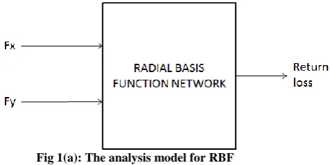
Radial basis function networks are very popular for their fast convergence in function approximation as compared to Back Propagation Neural Networks. In this work, the feed location of novel designed antenna is taken as input variables for learning of RBF networks while return loss is taken as output variable. The rest of parameters such as dielectric constant of substrate, height of substrate and resonant frequency are all considered constant while collecting samples for training and testing. The analysis model for this is shown in figure 1(a).
Samples have been taken using random feed locations for coaxial probe feeding technique in the proposed design using HFSS electromagnetic solver. Total 70 samples have been taken for training while 10 different samples were taken for testing for the purpose of checking the validation and accuracy of the trained neural network. The network is trained for different values of spread constant ranging from 0.01 to 10 in order to get optimum value of spread constant for desired purpose. The final spread constant is taken to be 0.01 that satisfied the desired accuracy of testing.
Fig 1(a): The analysis model for RBF
4.
ANTENNA LAYOUT & STRUCTURE
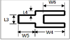
The structure of the proposed antenna design is to be studied in this section. Figure 1(b) represents the architectural view of the proposed antenna. This antenna is made up of three layers in which first layer comprises the conductive ground plane, second layer comprises the substrate i.e. dielectric material and third layer comprises the conductive patch. Simply we can say the circular patch antenna of specified dimensions is separated from the ground plane by a substrate of ‘Rogers RT/duroid 5880’ of finite thickness. Co-axial probe feed is preferred to analyze the antenna for better impedance matching. Slotted perturbations are employed in upper half of the circular patch antenna to transform the antenna characteristics from single band to multiband.
The dimensions of the slots are to be chosen through literature as well as iterative trials so that the proposed antenna geometry could be able to radiate at multi resonant frequencies. With this only one particular patch antenna is utilized for almost four applications as aforesaid. As the resonating characteristics of the rectangular patch depends upon its length and width similarly resonating characteristics of the circular patch depends upon the radius of the patch which is described from literature review, the effective radius of circular patch is found by [15]:
(1)
[image:2.595.331.569.328.447.2]h = height or thickness of the substrate εr = dielectric constant
The effective area of the patch is then given by [16]:
(2)
Fig 1(b): Geometry of proposed antenna
Fig 1(c): Elementary slotted structure 1
The effective radius and effective area of the proposed antenna are calculated by the equation 1 and 2. The effective radius of the circular patch is somewhat higher than the actual radius because of the fringing phenomenon in the microstrip patch antennas.
Fig 1(d): Elementary slotted structure 2
As the effective radius changes due to fringing, definitely there will be change in the area of the circular patch that actual area is to be calculated by equation 2. To enhance the antenna performance different slotted structures of figure 1(c) and figure 1(d) are embedded in the upper half of the proposed antenna as shown in figure 1(b).
The dimensions of the patch antennas are playing very important role in deciding the performance characteristics of the analyzed antenna. The initial dimensions are to be calculated as per the mathematical expression presented by [17] and further optimized values of all the parameters are obtained by having iterative trials on the software. All the optimized dimensions of the proposed antenna geometry are presented in the table 1 for the better understanding. The dimensions of the ground plane i.e. length and width of the ground plane are same as the length and width of the substrate
[image:3.595.60.261.107.406.2]material, therefore ground plane dimensions are not included in the table 1. The dielectric constant of the substrate material plays a vital role in deciding the resonant frequency as well as impedance bandwidth of the patch antenna is represented by the ‘εr’. Radius of the circular patch is represented by the ‘R’ and height of the substrate material is denoted by ‘h’ and their typical values are mentioned in table 1.
TABLE 1. Design parameters of the proposed antenna
Antenna parameter
Dimension Antenna parameter
Dimension
L 50.10 mm L4 1.00 mm
W 52.00 mm W1 13.00 mm
R 22.33 mm W2 5.00 mm
εr 2.2 W3 9.00 mm
h 1.58 mm W4 7.00 mm
L1 2.00 mm W5 4.00 mm
L2 1.00 mm W6 5.0 m
L3 2.00 mm
5.
RESULTS AND DISCUSSIONS
[image:3.595.311.549.172.380.2]In order to analyze the performance of the proposed antenna design, First of all the height of the Substrate should be selected so that proposed design must radiate at the specified frequencies. Variation in the substrate thickness is chosen according to the availability of the material in the international market. Figure 2 shows the response of the proposed antenna with respect to the frequency by varying the thickness of the substrate from 1.3 mm to 2.65 mm.
Fig 2: Return loss Vs. frequency plot of height variation of proposed antenna geometry
It is observed that with substrate thickness 1.3 mm antenna resonates at frequencies 6.4 GHz, 6.81 GHz and 8.18 GHz with return loss characteristics of -15.36 dB, -18.32 dB and -24.44 dB respectively and shown by black squared line in figure 2.
[image:3.595.311.549.175.379.2] [image:3.595.319.539.463.652.2] [image:3.595.96.239.487.569.2]antenna resonates at frequencies 6.51 GHz, 7 GHz and 8.25 dB with S11 ≤ -10dB of -19.82 dB, -11.12 dB and -18.56 dB respectively and shown by blue triangled line in figure 2.
Similarly the antenna performance is observed by varying the thickness upto 2.65 mm and observed that the substrate thickness of 1.58 mm is preferably opted as it provides the required return loss values at specified frequencies. Tabular form of results of return loss versus frequencies is presented in table 2 for more clarity.
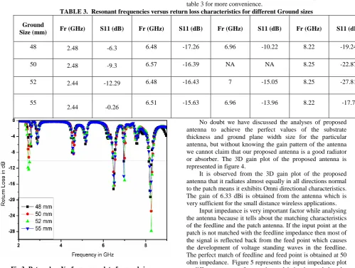
[image:4.595.315.559.69.190.2]Figure 3 represents the performance of the proposed antenna with different ground sizes varies from 48 mm to 55 mm. At ground width of 48 mm antenna resonates at frequencies 6.48 GHz, 6.96 GHz and 8.22 GHz with S11 ≤ -10dB values of -17.26 dB, -10.22 dB and -19.24 dB respectively and shown by black squared line in figure 3.
TABLE 2. Resonant frequencies and return loss characteristics at different thickness of substrate
Substrate height ( mm)
Fr (GHz)
S11 (dB)
Fr (GHz)
S11 (dB)
Fr (GHz)
S11 (dB)
1.3 6.4 -15.36 6.81 -18.32 8.18 -24.44
1.45 6.48 -16.43 7 -15.05 8.25 -27.81
1.58 6.51 -19.82 7 -11.12 8.25 -18.56
2.05 6.48 -14.22 6.85 -12.88 8.22 -13.89
2.65 6.51 -9.75 7.11 -8.84 8.22 -9.04
Further ground width increases to 50 mm and observed that return loss characteristics changes and only two resonating frequencies are found at 6.57 GHz and 8.25 GHz, which means antenna offers dual band performance at 50 mm ground size. The ground width increase to 52 mm and the performance of proposed design is shown by the green triangled plot of figure 3.
It is observed that at 52 mm antenna represents the multiband (quad band) characteristics at resonant frequencies 2.44 GHz, 6.48 GHz, 7 GHz and 8.25 GHz with the return loss S11 ≤ -10dB values of -12.29 dB, -16.43 dB, -15.05 dB and -27.81 dB respectively. Similarly antenna is analyzed for 55 mm ground width and the result is represented by triangled blue plot of figure 3. It is not easy to distinguish the performance of the antenna from the line plots presented in figure 3; therefore all these results are also represented in table 3 for more convenience.
TABLE 3. Resonant frequencies versus return loss characteristics for different Ground sizes
Ground
Size (mm) Fr (GHz) S11 (dB) Fr (GHz) S11 (dB) Fr (GHz) S11 (dB) Fr (GHz) S11 (dB)
48 2.48 -6.3 6.48 -17.26 6.96 -10.22 8.22 -19.24
50 2.48 -9.3 6.57 -16.39 NA NA 8.25 -22.87
52 2.44 -12.29 6.48 -16.43 7 -15.05 8.25 -27.81
55
2.44 -0.26 6.51 -15.63 6.96 -13.96 8.22 -17.7
Fig 3: Return loss Vs. frequency plot of ground size variation of proposed antenna geometry
No doubt we have discussed the analyses of proposed antenna to achieve the perfect values of the substrate thickness and ground plane width size for the particular antenna, but without knowing the gain pattern of the antenna we cannot claim that our proposed antenna is a good radiator or absorber. The 3D gain plot of the proposed antenna is represented in figure 4.
It is observed from the 3D gain plot of the proposed antenna that it radiates almost equally in all directions normal to the patch means it exhibits Omni directional characteristics. The gain of 6.33 dBi is obtained from the antenna which is very sufficient for the small distance wireless applications.
[image:4.595.56.307.355.720.2] [image:4.595.53.553.357.733.2]Fig. 4. 3D gain plot of proposed antenna geometry
[image:5.595.67.569.276.502.2]Fig 5: Input impedance Vs. frequency plot of proposed antenna geometry
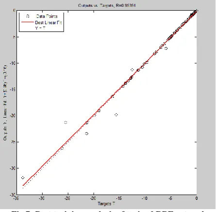
Fig 6: Training performance of RBF network After optimizing the design of proposed antenna, the
[image:5.595.316.539.510.729.2]design is analyzed using RBF neural network. Fig. 6 shows the training plot of RBF network taking feed location as input variable and return loss as output variable. The spread constant taken is 0.01 and final error goal is zero. After training, error performance has been reduced to 6.47* 10-5 which is quite acceptable. Fig. 7 shows the post training analysis to test the training efficiency of the learned network. It performs a linear regression between the network response and the target, and computes the correlation coefficient (R value) between the network response and the target.
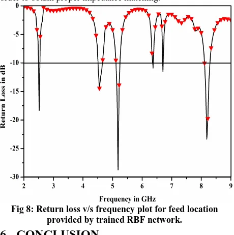
trained neural network is (8.65, 18.5) for x and y co-ordinates. The feed location obtained by trained RBF network resulted in the six band behavior at resonant frequencies ?? as shown in fig. 8.
[image:6.595.54.284.152.383.2]Thus, function approximation property of RBF neural networks serves an important alternative to trial and error method of finding optimum feed location for antennas in order to obtain proper impedance matching.
Fig 8: Return loss v/s frequency plot for feed location provided by trained RBF network.
6.
CONCLUSION
A novel circular patch antenna design is investigated and the parameters are chosen by mathematical as well as iterative trial with the simulation software. The analysed design exhibits multiband behaviour at different resonant frequencies of 2.44 GHz, 6.48 GHz, 7 GHz and 8.25 GHz with the return loss S11 ≤ -10dB values of -12.29 dB, -16.43 dB, -15.05 dB and -27.81 dB respectively. It is also observed that the proposed design offers a good value of gain of 6.33 dB and it is also matched at input impedance approximately equal to 50 ohm. The proposed antenna design is suitably recommended for the applications like WLAN (2.44 GHz at -12.29 dB), Radio astronomy (6.48 GHz at -16.43 dB ), Passive sensors (7 GHz at -15.05 dB) and Point to Point defence system (8.25 GHz at -27.81 dB) wireless applications. In addition, the optimum feed location is found by using function approximation of RBF neural networks. The solutions obtained using RBF networks are quite in good accord with the simulation results obtained using HFSS simulator.
7.
REFERENCES
[1] W. He, R.Jin and J. Geng, “E-Shape patch with wideband and circular polarization for millimeter-wave communication”, IEEE Transactions on Antennas and Propagation vol.56, no.3, pp. 893-895, 2008.
[2] Zhang, Y.P. and J.J., Wang. “Theory and analysis of differentially-driven microstrip antennas”, IEEE Transactions on Antennas and Propagation vol.54, no.4, pp.1092-1099, 2006.
[3] Mahmoud N. Mahmoud, Reyhan Baktur,“ A Dual Band Microstrip Fed Slot Antenna”, IEEE Transaction on
Antennas and Propagation, vol. 59, no. 5, pp. 1720-1724, May 2011.
[4] J. R. James, P. S. Hall, “Handbook of Microstrip Antennas", vol. 1, Peter Peregrinus Ltd., London, 1989. [5] K. M. Chen, Y. Huang, J. Zhang, and A. Norman,
Microwave life detection system for searching human subjects under earthquake rubble or behind barrier, IEEE Trans. Biomed. Eng., vol. 27, no. 1, pp. 105-114, Jan. 2000.
[6] S. Agata and S.H.David, “Novel Printed Bow-Tie Antennas for Dual-Band Dual-Mode Mobile Handsets”, IEEE, London, UK, 1998.
[7] S.K. Behera, R.K. Mishra, and D.R. Poddar, “Balanced amplifying microstrip patch antenna at 2.4 GHz”, IEEE Applied Electromagnetics Conference, AEMC 2007, pp. 1-4, Kolkata, Dec 2007.
[8] O. Losito, “High Efficiency and Broadband Microstrip Leaky-Wave Antenna”, Active and Passive Electronic Components, vol. 2008, Article ID 742050, pp. 1-6, 2008.
[9] M.T. Islam, M.N. Shakib, and N. Misran, “Broadband Microstrip Patch Antenna”, European Journal of Scientific Research, vol.27, no.2, pp.174-180, 2009. [10]A. Keshtkar, Ahmed Keshtkar and A. R. Dastkhosh,.,
“Circular Microstrip Patch Array Antenna for C-Band Altimeter System” , International Journal of Antennas and Propagation, vol. 2008, Article ID 389418, pp. 1-7, 2008.
[11]T.F. Lai, W.N.L Mahadi, and N.Soin , “Circular Patch Micro strip Array Antenna for KU-band” World Academy of Science, Engineering and Technology, pp. 48, 2008.
[12]V. Thakare and P. Singhal, "Artificial Intelligence in the Estimation of Patch Dimensions of Rectangular Microstrip Antennas," Circuits and Systems, Vol. 2 No. 4, 2011, pp. 330-337. doi: 10.4236/cs.2011.24046. [13]V.V. Thakare, S. S. Jadon, and R. Kumari, “Analysis of
Circular Microstrip Patch Antenna Using Radial Basis Artificial Neural Network”, International Journal of Electronics and Computer Science Engineering, Vol. 1, No. 3, pp. 901-905, 2013.
[14]M.S.Alam, M.T. Islam, N. Misran,"Design analysis of an electromagnetic band gap microstrip antenna", Am. J. Applied Sci., Vol. 8, Issue 12 , 2011.
[15]C.J. Kaufman, Rocky Mountain Research Lab., Boulder, CO, private communication, May 1995.
[16]Y. Yorozu, M. Hirano, K. Oka, and Y. Tagawa, “Electron spectroscopy studies on magneto-optical media and plastic substrate interfaces(Translation Journals style),” IEEE Transl. J. Magn.Jpn., vol. 2, Aug. 1987, pp. 740–741 [Dig. 9th Annu. Conf. Magnetics Japan, pp. 301, 1982.