Stability Analysis of DC-DC Boost Converter for Solar
Electric Application
Suraj Sharma Subedi
Electrical and Electronics Engineering Department Sikkim Manipal Institute of
Technology, East-Sikkim
Amir Ahmed
Electrical and Electronics Engineering Department Sikkim Manipal Institute of
Technology, East-Sikkim
Prateik Raj Chettri
Computer science and Engineering Department Sikkim Manipal Institute of
Technology, East-Sikkim
ABSTRACT
The main focus of this paper is to do simulation, modeling and stability analysis of DC-DC Boost converter for Solar Electric system. The open loop dc-dc boost converter uses 12 Volt dc supply from a solar panel and converts it into 24 Volt dc output which can be used for various solar electric applications for e.g to run a motor using an inverter. The stability analysis includes time domain analysis, frequency domain analysis and pole-zero domain analysis using state space averaging technique. The simulation and stability study is done using MATLAB from its respective graphs obtained from above mentioned domains.
General Terms
DC-DC Boost Converter, open loop, MATLAB, Stability analysis, , state space averaging technique.
Keywords
Frequency domain, pole-zero, time domain,eigen,routh’z criterion
1.
INTRODUCTION
Emerging need of renewable sustainable source of energy has resulted in advancement of numerous solar electric applications. DC-DC converters are considered to be of great economical importance in today’s society, and are perhaps one of the few electronic circuits that are commonly used in switching power supplies. The solar energy conversion systems can be connected to a large electrical transmission grid, or to the storage or auxiliary energy supply[1]. To obtain a stable voltage from an input supply (PV cells) that is higher and lower than the output, a high efficiency and minimum ripple DC-DC converter required in the system for residential power production.
[image:1.595.328.535.210.319.2]The voltage level from a solar input voltage is raised to a higher level for the applications which demands a higher voltage level. The simulation model of the converter uses the designed parameters for the voltage conversion. The demand for energy, particularly in electrical forms, is ever-increasing in order to improve the standard of living. The dc-dc converters can be viewed as dc transformers that deliver to the load a dc voltage or current at a different level than the input source. This dc transformation is performed by electronic switching means, not by electromagnetic means such as in conventional transformers[2]. Here, MATLAB simulation of the proposed converter provides stronger evidences about its stability, and the usefulness when applied to the solar electric systems. The block diagram of solar electric system is shown in Figure 1.[3]
[image:1.595.314.566.372.707.2]Figure 1. Block Diagram of Solar Electric System.
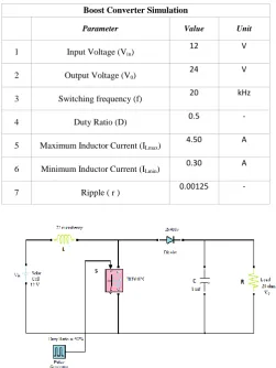
Table 1. Parameters for Boost Converter simulation.
Boost Converter Simulation
Parameter Value Unit
1 Input Voltage (Vin)
12 V
2 Output Voltage (V0)
24 V
3 Switching frequency (f) 20 kHz
4 Duty Ratio (D) 0.5 -
5 Maximum Inductor Current (ILmax)
4.50 A
6 Minimum Inductor Current (ILmin)
0.30 A
7 Ripple ( r ) 0.00125 -
2.
STATE SPACE AVERAGING
TECHNIQUE
L = inductance in the circuit.
C = capacitance in the circuit.
D = duty cycle.
f = switching frequency.
RI = parasitic resistance of an inductor.
R2= parasitic resistance of a capacitor.
Vin = input solar voltage to the converter.
Lb= boundary value for inductance.
Cmin= minimum capacitance required for continuous conduction mode.[4]
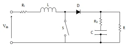
Figure 3. Circuit design of boost converter.
In the above circuits, S is the electronic high speed switch (that is supposed to be ideal), D the diode, C the capacitor, L the inductance, and the load , for simplicity, is taken to be ohmic and is denoted by the resistance R. When the switch S is in the on state, the current in the boost inductor increases linearly and the diode D is off at that time. When the switch S is turned off, the energy stored in the inductor is released through the diode to the output RC circuit[6].
For Continuous Conduction Mode (CCM), the value of L and C should be greater than Lb (=62.5 microhenry) and Cmin (=125 microfarad if ripple considered is 1%) respectively. Since it is assumed that the converter is operated in continuous conduction mode, two different systems must be considered. The state-space description of each one of these two systems is derived as given below.
The current flowing through an inductor and the voltage across the capacitor is taken as state variables for obtaining the state space model of dc-dc boost converter.
2.1
When Switch is on
The State Space Model Equation:
X = A1x + B1 Vin.
Y = C1x.
[image:2.595.62.280.311.394.2]2.2
When Switch is off
Figure 5. Configuration of the converter for S off.
The State Space Model Equation:
X = A2x + B2 Vin.
State-space averaging (Middlebrook and Cuk, 1976) is one method to approximate this time-variant system with a linear continuous time-invariant system[5]. Now, state-space descriptions are then averaged with respect to their duration of the switching period. For D= 50 % using state space averaging technique we get the following matrices.
3.
MATLAB Simulink Model
Figure 6. MATLAB Simulink Model.
4.
MATLAB SIMULATION
WAVEFORMS AND PRACTICAL
WAVEFORMS
[image:3.595.136.542.69.689.2]4.1
MATLAB Simulated Waveform
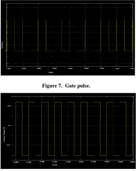
Figure 7. Gate pulse.
Figure 8. Inductor Voltage.
Figure 9. Inductor voltage and Inductor current waveform.
[image:3.595.316.547.72.362.2] [image:3.595.55.274.219.592.2]Figure 11. Output voltage and current Waveform.
[image:4.595.316.523.206.332.2]4.2
Practical Waveforms
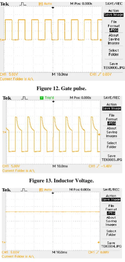
Figure 12. Gate pulse.
Figure 13. Inductor Voltage.
5.
MATLAB Analysis
5.1
Time Domain Analysis:
Any system will exist only in the time domain. However response viewed in time domain can also be viewed in frequency domain or pole-zero domain which are used to explain excitation capability, decay of the noises, disturbances and sinusoids which affects the output[8]. Here we can see an attainment of steady state value with zero overshoot.
There is no peaking observed in the step response of the above circuit, which attains a constant value with no transients in it.
Figure 15. Step Response of the system.
5.2
Pole-zero Domain Analysis:
Basically s-plane is the representation of the physical system that gives an idea about poles, location of poles, zeroes, location of zeroes of the system. In fact a pole in time domain is nothing but an exponential behavior which can be of increasing or decreasing in nature.
[image:4.595.63.274.275.716.2] [image:4.595.317.543.606.742.2]5.3
Frequency Domain Analysis:
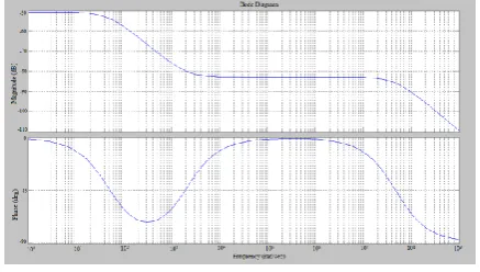
The Decibel-Gain plotted against frequency and phase plotted against logarithmical scale of frequency concludes that the system analyzed above is stable with infinite gain and phase margin since the phase crossover point as well as gain crosses over point cannot be determined.
[image:5.595.56.275.222.346.2]Phase crossover point in the bode plot is the point at which phase plot intersects with the -180° horizontal line. The frequency corresponding to the point of intersection is called phase crossover frequency. Gain cross over point in the bode plot is the point at which magnitude plot intersects with the 0 dB line. The frequency corresponding to the point of intersection is called the gain crossover frequency.
Figure 17. Bode Plot
6.
CONCLUSION
1. In case of a boost converter the output voltage ripple can be limited by the use of a larger filter capacitor in comparison to that in the buck-derived converters. The filter capacitor must provide the output dc current to the load when the diode D is off. The minimum value of the filter capacitance that can be used is 125 microfarad (considering ripple as 1%). The end result is that the value of L and C are much larger than those of a buck regulator. High value of capacitance is used in order to reduce output ripple in the designed system[9].
2. From simulation it is evident that the use of higher switching frequency reduces the size of inductor for the same value of ripple current and filtering requirement.
3. Transfer function for the above system is 3415 s + 6.825e06
s2 + 4.781e07s + 2.336e09
4. Rouths- Hurwitz Stability Criterion: It is an algebraic procedure that provides information on the absolute stability
of a LTI system using its characteristic polynomial. It was verified that all the elements of the first column of the array was positive which indicated all the roots of the characteristic equation were located in the left half of s-plane. Thus, providing BIBO stabilility for the proposed system.
5. Eigen Values: The Eigen value obtained for the system are negative real number which implies the system shall be driven back to its steady state value by an exponential decay mechanism.
ACKNOWLEDGMENTS
We would like to offer our sincere gratitude to Sikkim Manipal Institute of Technology’s Electrical and Electronics Department for allowing us to pursue our research. Our special thanks and gratitude goes to our guide and mentor - Dr. K.S Sherpa for incessantly offering us a share of his vast knowledge and sparing his precious time to teach us new things.
7.
REFERENCES
[1] Diary R. Sulaiman, Hilmi F. Amin, Ismail K. Said. Design of High Efficiency DC-DC Converter for Photovoltaic Solar Home Applications.
[2] Muhammad H. Rashid. 2001. Power Electronics Handbook. University of West Florida Pensacola, Florida, 01-223.
[3] Asmarashid Ponniran , Abdul Fatah Mat Said.” DC-DC Boost Converter Design for Solar Electric System”. [4] Fabio De Filippo and Francesco Vasca, “DC/DC
Converters”.
[5] Bengt Johansson. 2004. DC-DC Converters -Dynamic Model Design and Experimental Verification, Lund University, Sweden, 100-115.
[6] Muhammad H. Rashid. 2003. Power Electronics Circuits, Devices, and Applications, 3rd. ed. University of West Florida.: Pearson Prentice Hall, 166-224.
[7] Fraidoon Mazda. 1997. Power Electronics Handbook, Third Edition, , 261-282.
[8] M.Gopal, Control System: Principle and Design, 773-790.
[9] G.K Dubey. 1995. Fundamentals of Electrical Drives 37-51.