High Performance Asynchronous Pipelined
QDI Templates for DCT Matrix-Vector Multiplication
D.Jayanthi
Associate Professor, Dept. of ECE, Sona College of Technology, Salem.
M.Rajaram
Vice-Chancellor
Anna University of Technology, Tirunelveli.
ABSTRACT
The mass application of asynchronous design has been an elusive goal for academic researchers while recent advances are promising. However asynchronous circuit has some inherent advantages over synchronous counterpart. The matrix – vector multiplication core of discrete cosine transforms (DCT) is demonstrated in this paper, by non linear pipelined templates. From this proposed DCT applications, Quasi-Delay Insensitive (QDI) templates are introduced to yielding average high performance and low power. Novel control circuit templates have been used to simplify the design of such non linear pipelines.QDI circuits are quite robust in terms of process variations and design tolerances. Our proposed asynchronous design yields 35% higher average throughput and negligible energy overhead compared with conventional synchronous design.
Keywords
Asynchronous channels, control circuit templates, discrete cosine transforms, matrix vector multiplication, Pre-Charged Full Buffer, Reduced Stack Pre-Charged Half Buffer.
1. INTRODUCTION
Asynchronous design which replaces [1] global clocking local handshaking has the potential to make high speed design more feasible. Asynchronous design has recently attracted industry [2] [3] due to its potential for low power consumption, low electromagnetic interfaces, high speed and robust interfacing. The focus of this paper is on a key enabling technology to make high speed asynchronous system practical, and the design of high throughput asynchronous pipelines. The two dimensional (2-D) discrete cosine transform (DCT) and inverse DCT IDCT) are vital tasks[4] in data compression and decompression standards, such as H.261, H.263, JPEG,
and MPEG.Low-power and high performance
implementations of the DCT and IDCT are simultaneously increase in need for faster data rates and longer battery lifetimes in portable multimedia devices are progressively more essential. A matrix-vector multiplier, naturally[4] [7]executed with a set of multiply-accumulation unit, a core operation inside both of these applications is the multiplication of a constant matrix by an input vector. Many DCT/IDCT synchronous and asynchronous designs have been explored targeting high-performance [5], [6], [8], low-power [9], [10], or both [11]. Xanthopoulos et al. observed that [4] on average of a significant fraction of IDCT input data is zero valued. This encouraged the growth of a data-driven IDCT that skips operations involving zero-valued data, thus saving power. To also take advantage of small-valued data, Canel et al. and Nielsen et al. Proposed data compression [9], [10] process that continue only considerable data portions and suppress the residual trivial portions. These designs yield low average power but, because they are synchronous, offer no
average-case performance profit. A QDI system is constructed as a collection of concurrent hardware modules (called processes) [12] that communicate with each other through message-passing channels. These messages consist of atomic data items called tokens, which are usually multi-rail encoded each process can send and receive tokens to and from other processes through one-to-one communication by means of handshake protocols. Due to the lack of global clock and multi-rail encoded data communication, QDI circuits have the potential to achieve self-checking and halt the circuit in the presence of failures. An asynchronous width adaptive data architecture that [13] activates operations only in significant data portions and adjusts the position of sign bit dynamically. This architectural approach [14] yields good average-case performance and reduces power consumption, but the representative implementation is based on the quasi-delay-insensitive asynchronous design style, which is known to be area expensive.
2. Asynchronous Channel
Both two and four phase handshaking protocols are present across communication channels.
3. MATERIALS AND METHODS
PCFB: The Fig. 2 below shows the templates for Pre-Charged Full Buffer (PCFB).This input end completion detector is denoted by LCD and while its output end completion detector is denoted by RCD. The PCFB is more concurrent than the PCHB (Pre-Charged Half Buffer) based on its L and R handshakes reset in parallel at the cost of requiring an additional state variable.
Fig 2: PCFB
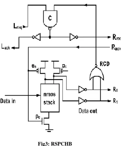
The new QDI pipeline template is referred to as a Reduced Stack Pre-Charged Half Buffer (RSPCHB) as shown in Fig3.It is noted that the RCD block is optimized by tapping its inputs before the output inverter and a NAND gate is used instead of an OR gate.
Fig3: RSPCHB
RSPCHB template facilitates the removal of the internal enable signal by reducing concurrency that does not improve
performance. In the PCFB templates the output of LCD and RCD are companied using a C-element to generate acknowledgment signal Lack. As a result integration of the handshake protocol with the validity and neutrality of both input and output data is supported .This gets rid of the need for function block to be weak conditioned .Though requires the use of the en signal, this replacement introduces more concurrent than is necessary. In the case of a join, the non weak conditioned function block may generate an output when one of the input channels provides data. Therefore the RCD of the join asserts its output. On the other hand any subsequent stage can receive data, evaluate asserts both its LCD and RCD outputs and asserts acknowledgment signal. Though the join can receive acknowledgment, it will not precharge until after en is asserted. After the acknowledgment to the input stages has been asserted the en signal delays the precharge of the circuit. This delay prevents the precharge from triggering the RCD to deassert. The en signal could be safely removed if generation of acknowledgment signals from any stage subsequent to the join has arrived and been acknowledged .The join been the performance bottleneck for the subsequent stages, delay of the acknowledgment would not impact performance. The advantage of RSPCHB is that the lack of an LCD and reduced stack size of the function block, which reduces capacitive load and yields significantly faster overall performance.
[image:2.595.59.268.486.736.2]Fig4: STG of the abstract PCFB protocol
Fig 4 shows the STG of (signal transition graphs) when a left token arrives (L+), the R_gen dynamic logic blocks evaluate, produces a valid output token, the local clock will fire ( R i - r R i+), and at the same time the iLCD block sense the
deassert the right enable (Re-), allowing the R_gen blocks to precharge. This allocates the right environment to reassert the right enable (Re+) and , concurrently, the internal enable to be reasserted (en+).This in turn allocate the R_gen blocks to re-evaluate in respond to a new token.
Fig5: STG of the abstract RSPCHB protocol
The analytical expression for the timing margin associated with this isochronic fork assumption can be derived from the abstract STG of the RSPCHB shown in Figure 3. Where F1 e represents the Function F1 at evaluation state, F1P represents
the Function F1 at pre-charge state, C1+ represents the completion detector C1 changes its state to 1, C1- represents the completion detector C1 changes its state to 0, RCD+ represents the Right Completion Detector RCD changes its state to 1 and RCD- represents the Right Completion Detector RCD changes its state to 0 of pipeline stage 1.
4.
MATRIX–VECTOR
MULTIPLICATION ARCHITECTURE
In this section, we review matrix multiplication operation and discuss our proposed architecture in detail.
4.1 Matrix–Vector Multiplication
Here an another study of matrix multiplication operation and explains our proposed architecture in detail. The matrix– vector specification that the implementations can be expressed as follows:
4.2 Asynchronous Pipelined Architecture
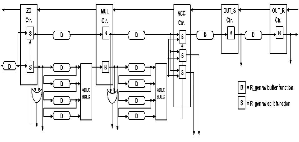
Two novel speculative delay matching controller are involved in Matrix Vector multiplication. One for an asymmetric delay line controller (ADLC) and one for a symmetric delay line controller (SDLC).Each controller functions same as to one of its output signals based on the select control lines. Both delay line controllers are compact and the power is significantly reduced. At the algorithmic level, the basic strategy of implementing each matrix vector multiplication in four iterations has been taken, one per column of the matrix. In iteration, the ith column is multiplied by the ith element of y. This occupies multiplying an input with three different coefficients and possibly inverting the result, thereby motivated as the use of three distinct hardwired multipliers. Accumulators are used to stores the results of each iteration, whose results are written to after the fourth iteration and then reset in preparation of the next input vector. At the architectural level, we propose the novel five-stage pipelined
architecture shown in Fig. 8. The upper portion of the picture explains asynchronous controllers communicated with the datapath and other controllers with four-phase handshaking signals rather than a global clock. To obtain low power, the datapath is executed using single-rail static logic. Numerous power optimizations looking advantages of small-valued input statistics are applied. The general idea is to dynamically deactivate groups of bit-slices that contain only sign extension bits (SEBs). In the datapath, the MASK unit identifies the bit-slices of input data that contains non-SEBs and the zero data unit (ZDU) detects the special case in which the data is zero. If the input data is zero, the ZDU unit asserts a zero_detect signal that disables the entire computation operations. To handle nonzero input data, the multipliers and accumulators consist of groups of partitioned bit-slices that are selectively activated by the MASK unit. In particular, the mask signals are used to deactivate non-SEBs by forcing them to zero via the input ANDing logic and are sent to control matched delay lines in the multiplier stage. Additionally, the same mask signals when latched are ORed with their previously registered versions. The resulting mask signals (OR ) identify the bit-slices of the accumulators that contain non-SEBs and matched delay lines in the accumulator stage. The result of the accumulator stage is fed to the partial sign bit recovery (PSBR) logic which expands the sign bit of newly activated bit-slices in the accumulator to ensure that both inputs to the accumulator have the same number of activated bit-slices. in the last iteration, the full sign bit recovery (FSBR) logic improves the suppressed zero bits of accumulator results to get the correct final result. Our fine-grain hardwired multiplier is based on a bit-partitioned carry-save multiplier, illustrated in Fig. 7. The carry-save multiplier’s critical path is mainly by the side of the final, vector-merging adder, which we executed as a bit-partitioned ripple–carry adder for two reasons. First, ripple-carry adders consume significantly lower power than faster (e.g., carry select or bypass) adders. Secondly, while ripple-carry adders have relatively long worst case delay, the bit-partitioning of the multiplier array (including the ripple-carry adder) leads to very good average case delay for this application. The staircase-patterned bit-slices, as illustrated by the dotted lines in Fig. 7, agree to the adders to be dynamically configured for different input bit-widths. For example, if the first two bit-slices are make actived, the multiplier behaves exactly as a typical multiplier that handles 9-bit inputs.
4.3 Controller Alternatives
Fig 7. Proposed asynchronous fine grained carry-save hardwired multiplier
[image:5.595.53.532.433.660.2]0
1 1
2 2
3 3
o
z x x x x y
z v u u v y
z x x x x y
u v v u
z y
0 1 2 3
0 1 2 3
0 1 2 3
0 1 2 3
( ) ( ) ( ) ( )
( ) ( ) ( ) ( )
( ) ( ) ( ) ( )
( ) ( ) ( ) ( )
x y x y x y x y
v y u y u y v y
x y x y x y x y
u y v y v y u y
4.4 Performance Metrics
To compare among different synchronous/asynchronous designs, the following metrics are used to analyze the performance of bundled-data pipelines.
1) Forward latency (FL) is defined as the delay of the request of the current stage to the request of the next stage. In other words, it indicates the evaluation time of the datapath. 2) Overhead (OH) is defined as the delay beginning from the request of the next stage to the next request of the
current stage. In other words, it is the overhead associated with resetting the control circuits.
3) Cycle time is defined to be the maximum delay
5. DESIGN FLOW, EXPERIMENTAL
RESULTS, ANDCOMPARISONS
The hierarchical design flow have been used in our design. First step shows, after behavioral specification of the design is précised,each behavior block in verilog describe a constructed architectural specification. At this step, simulation is used to verify functional correctness of our architecture. Next, gate-level Verilog is decomposed each block. Following that transistor-level implementation is to map each gate in our library. A set of transistor-level simulations is performed to verify that all timing constraints and to ensure correctness are met. The final step a layout is generated hierarchically. At this step, timing analysis and correctness are executed by extracting wire capacitance and thus considering the impact of interconnection delays.
5.1. Throughput and Energy Comparisons
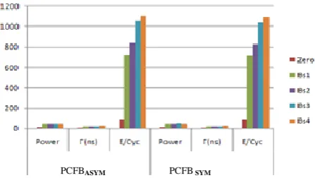
The first work evaluate asynchronous designs using the PCFB control with two different delay lines, a standard asymmetric delay line (PCFBASYM ) compare with one using the power efficient delay line (PCFBSYM ).Our designs uses five different inputs which activates zero to all bit-slices and the simulation results are verified.
Table 1. Comparison of PCFB based designs using Different Asymmetric Delay Lines
Table 1 exhibits average power, cycle time, and energy per cycle. The result propose that the performance of design using (PCFBSYM ) controls and yields up to 2.2% lower energy than (PCFBASYM ) control. However the controller put in as little as 4.8 % of the overall energy, the (PCFBSYM ) controller yields up to 46% lower energy than the (PCFBASYM ) controller. Therefore, we prefer the (PCFBSYM ) control as the nominated design using PCFB control for the follow up evaluations.
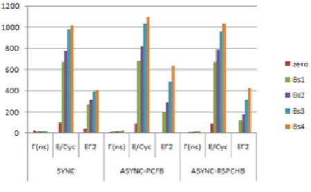
[image:6.595.54.264.71.201.2]Next, Table 2 shows the design compares two different asynchronous designs: one using PCFB controllers and another one using RSPCHB controllers. Table III illustrates the worst case forward latency (FL),
Table 2. Comparison of PCFB and RSPCHB based on timing analysis, forward latency, Overhead and Cycle
Time
cycle time (г) , and controller overhead (OH) of two designs for each type of inputs from zero to all bit-slices activated. The result implies that the RSPCHB template is consistently operate 19–38% faster than PCFBs. Furthermore, the worst case latency of the accumulators is 18.8 ns, and we set the synchronous cycle time to 20 ns. To quantify performance power tradeoff, we set up ten test cases as follows. The first seven test cases, each having 20 input vectors, are simulated using Nanosim on the extracted layout. Of these, the first five test cases demonstrate average cycle time and energy comparison of zero data and four different bit-slices activated starting from zero data and then bit-slice one (bs1) to bit-slice four (bs4).
TEST PATTEREN
SYNC ASYNC-PCFB ASYNC-RSPCHB
Г(ns) E/Cyc рJ
EГ2 Г(ns) E/Cyc рJ
EГ2 Г(ns) E/Cyc рJ EГ2 Zero Bs1 Bs2 Bs3 Bs4 20 20 20 20 20 95 671 775 981 1015 39 270 311 394 407 6.9 16.6 18.6 21.5 22 91 686 817 1036 1098 5.6 194 290 489 634 4.4 12.9 14.8 17.9 20 89 672 785 961 1035 2.9 116 178 314 424 TEST PATTEREN
PCFB ASYM PCFB SYM % of
Lower Overall energy % of Lower controller energy Power mW
Г(ns) E/Cyc Power mW
Г(ns) E/Cyc
Zero Bs1 Bs2 Bs3 Bs4 11.5 42.5 45.3 44.5 45.4 7.2 16.4 18.4 21.6 23.7 91.5 721 842 1054 1108 12.1 41.7 42.9 46.8 44.5 6.9 16.6 18.6 21.7 23.8 91.3 714 824 1036 1092 0.14 0.8 1.8 1.7 1.5 5 13 27 33 28
[image:6.595.326.550.186.312.2]Table 3. Comparison of PCFB and RSPCHB based design (Control and Datapath) with detailed Timing and
energy Analysis
The experimental results are described in Table 3. The first two columns for each design show the cycle time (г)and energy per Cycle(E/cyc) . The third column for each design specifies the Eг2
[15] product compared to the synchronous design. The results direct to the following points. First, since the identical datapath is applied to all designs, the energy differences are due to the difference in energy consumed by the controllers. The clock-gating synchronous controller consumes the least energy, followed by the asynchronous RSPCHB controller, and followed by the asynchronous PCFB. Additionally, the results show the effectiveness of bit-slice partitioning in that a smaller bit-bit-slice consumes less energy than a larger one. In particular, a zero input data consumes far less energy than the others. Second, it is obvious that in the asynchronous designs a smaller bit-slice operates faster than a larger one. However, due to its large control overhead, the PCFB controller loses its speed advantage over the synchronous design when more than two bit-slices are active while the RSPCHB controller is only slower when all bit-slices are active. Furthermore, the results of the bound analysis suggests that compared to the synchronous design, the cycle time of RSPCHB design is between 16%–35% faster and the cycle time of the PCFB falls somewhere between 6% slower and 13% faster. Lastly, the simulation with the three real images indicates that the typical performance gain over synchronous design is approximately 35% for the RSPCHB -based design and 10% for the PCFB--based design. Third, the asynchronous designs can tradeoff performance for low power. Without voltage scaling, our designs gives 14%–35% higher performance with a 3.5%–10.5% energy penalty. If the power supply is scaled, energy can be quadratically reduced. We adopt the Eг2
metric to quantify this advantage. The results show that, compared to the synchronous counterpart, the PCFB-based design has an 17% Eг2 advantage while RSPCHB -based designs have up to a 52% Eг2 advantage.
6. CONCLUSION
This paper demonstrates the use of an efficient asynchronous bundled-data pipeline design methodology on matrix–vector multiplication for DCTs. Architectural optimizations that take advantage of zero and small-valued data, typical in DCT and IDCT, yield both high average performance and low power. Novel control circuit templates and data-dependent delay lines are proposed to create low overhead integrated control circuits capable of handling nonlinear pipelines and enabling high average throughput. The results of the bound analysis suggests that compared to the synchronous design, the cycle time of RSPCHB design is between 16%–35% faster and the cycle time of the PCFB falls somewhere between 6% slower and 13% faster. Lastly, the simulation with the three real images indicates that the typical performance gain over synchronous design is approximately 35% for the RSPCHB -based design and 10% for the PCFB-based design. Third, the asynchronous designs can tradeoff performance for low power. Comparisons with comparable gated-clocking synchronous counterpart suggest that the proposed asynchronous design yields 30% higher throughput with negligible energy overhead and has a 49% better metric.
7. REFERENCES
[1]. D.M.Chapiro,
Globally-Asynchronous,Locally-Synchronous Systems, Ph.D. dissertation, Stanford Univ., Stanford, CA, 1984, Stanford CS Tech. Rep. STAN-CS-84-1026.
[2]. LARS S. NIELSEN AND JENS SPARSO, Designing Asynchronous Circuits for Low Power:An IFIR Filter Bank for a Digital Hearing Aid, proceedings of the ieee, vol. 87, no. 2, February 1999.
[3]. J. Cortadella et al., Logic Synthesis of Asynchronous Controllers and Interfaces. New York:Springer-Verlag, 2002.
[4] K. Rao and P. Yip, Discrete Cosine Transform, Algorithm, Advantages, Applications. New York: Academic, 1990.
[5] A. Madisetti and A. W. Jr, “A 100 MHz 2-D DCT/IDCT processor for HDTV applications,” IEEE Trans. Circuits Syst. Video Technol., vol. 5, no. 2, pp. 158–165, Apr. 1995.
[6] S. Uramoto, Y. Inoue, A. Takabatake, J. Takeda, Y. Yamashita, M. Terane, and M. Yoshimoto, “A 100 MHz 2-D discrete cosine transform core processor,” IEEE J. Solid-State Circuits, vol. 36, no. 4, pp. 492–499, Apr. 1992.
TEST PATTEREN
PCFB RSPCHB %
FAST VS PCFB FL
Ns
Г(ns) OH ns
FL ns
[7] T. Xanthopoulos and A. P. Chandrakasan, “A low-power IDCT macrocell for MPEG-2 MP@ML exploiting data distribution properties for minimal activity,” IEEE J. Solid-State Circuits, vol. 34, no. 5, pp. 693–703, May 1999.
[8] R. Manohar, “Width-adaptive data word architectures,” in Adv. Res. VLSI, 2001, pp. 112–129.
[9] R. Canal, A. Gonzalez, and J. Smith, “Very low power pipelines using significance compression,” in Proc. MICRO’33, Dec. 2000, pp.181–190
[10] L. S. Nielsen and J. Sparsø, “Designing asynchronous circuits for lowpower: An IFIR filter bank for a digital hearing aid,” Proc. IEEE, vol. 87, pp. 268–281, Feb. 1999.
[11] K. Kim, P. A. Beerel, and Y. Hong, “An asynchronous matrix–vector multiplier for discrete cosine transform,” in Int. Symp. Low Power ElectronicsDesign, Jul. 2000, pp. 256–261.
[12] LaFrieda, C. and R. Manohar, 2009. Reducing power consumption with relaxed quasi delay-insensitive circuits. Proceedings of the 15th IEEE Symposium on Asynchronous Circuits and Systems, May 17- 20, IEEE Xplore Press, Washington, USA, pp: 217-226. DOI: 10.1109/ASYNC.2009.9.
[13]. AlainJ.Martin ,Asynchronous Techniques for System-on-Chip Design, Vol. 0018- 9219_2006.IEEE 94, No. 6, June 2006 , Proceedings of the IEEE.
[14] R. Manohar, “Width-adaptive data word architectures,” in Adv. Res.VLSI, 2001, pp. 112–129.
[15] J. Teifel, D. Fang, D. Biermann, C. Kelly, and R. Manohar, “Energy-efficient pipelines,” in Proc. Int. Symp. Advanced Research Asynchronous Circuits Systems, Apr. 2002, pp. 23–33.