http://dx.doi.org/10.4236/sgre.2014.510022
Modeling the Chain of Conversion for a PV
System
Mohammed El Alami
1, Mohamed Habibi
1, Seddik Bri
21Laboratory of Systems and Telecommunications Engineering Decision, Sciences Faculty, Ibn tofail University, Kenitra, Morocco
2Electrical Engineering Department, High School of Technology, Moulay Ismail University, Meknes, Morocco Email: [email protected]
Received 1 August 2014; revised 29 August 2014; accepted 8 September 2014
Copyright © 2014 by authors and Scientific Research Publishing Inc.
This work is licensed under the Creative Commons Attribution International License (CC BY). http://creativecommons.org/licenses/by/4.0/
Abstract
In this work, we conduct a study of modeling and simulation of a system in the context of renewa-ble energy in general, and solar system “photovoltaic” in particular; also, the optimizing system adapted by DC-DC converters static. Then the influence of temperature and irradiance on the op-timal parameters (Power of MPP, VMPP, ...) of a solar system is analyzed in a way to operate a PV generator at its maximum power. This system includes a photovoltaic generator, “Boost & Buck”, converter and a load. Modeling and simulation system (solar panel, DC-DC converter command and load) is obtained through Matlab-Simulink software.
Keywords
Photovoltaic Panel, DC-DC Converter, The Maximum Power Point, Fill Factor
1. Introduction
The use of solar energy will provide electricity to isolated sites of electrical networks and avoid the creation of new electrical lines which generally requires a heavy investment.
2. Modeling of the Photovoltaic System
The PV cell, also called solar cell, constitutes the basic element of the photovoltaic conversion. This is a semi-conductor device that converts electric energy into light energy provided by an inexhaustible source of energy and the Sun. It exploits the properties of semiconductor materials used in the electronics industry: diodes, tran-sistors and integrated circuits. Figure 1 illustrates a typical PV cell where its formation is detailed. The perfor-mance of energy efficiency achieved industrially are 13% to 14% for the cells based on monocrystalline silicon, with 11% to 12% of poly crystalline silicon and finally 7% - 8% for the amorphous silicon by thin films [2]. The photopile or solar cell is the basic element of a photovoltaic generator, and the equivalent circuit of a PV cell is shown in Figure 2. It includes a current source, a diode, a series resistance and a shunt resistance.
The photovoltaic effect is manifested when a photon is absorbed in a semiconductor material composed of doped p (positive) and n (negative), referred to as p-n junction (or n-p). Under the effect of doping, an electric field is present in the material permanently (like a magnet which has a permanent magnetic field) [3]. When an incident photon (grain of light) interacts with the electrons in the material, it transfers its energy to the electron hv which finds herself liberated from its valence band and therefore suffers the intrinsic electric field. Under the influence of this field, electron migrates toward the top surface leaving a hole that migrates in the reverse direc-tion. Electrodes placed on the upper and lower surfaces allow the electrons to collect them and to make electrical work to join the anterior surface of the hole. A cell is often modeled by the electrical equivalent diagram it is he that is shown in Figure 2, the photovoltaic generator is modeled by the following equations [4]:
. .
exp 1
. .
s s
ph s
sh
V I R V I R
I I I q
A K T R
+ + = − − −
(1)
. .
exp 1
. .
s s
ph s
sh
V I R V I R
P V I I q
A K T R
+ + = ∗ − − −
(2)
Electric Voltage
Front Contact
Back Contact
Sunlight
n-layer (electon conductivity)
p-layer (hole conductivity) n-p Junction
(electric Field)
0.5μ 300μ
Figure 1.Schématic of a photovoltaic cell.
Iph
ID
D
I
V Rserie
Rshunt RLoad
with Iph
( )
A is currently produced by the cells; Is( )
A is the saturation current;19
1
6 C
1. 0
q= × − load elec-tron; K=1.38×10⁻²³ J K/ Boltzmann constant; T (˚C) is the operating temperature of the cell; A is a quality factor of the diode, normally between 1 and 2; Rs
( )
Ω and Rsh( )
Ω are series and parallel resistors. After the determination of the various parameters of the equivalent circuit, it is possible to solve the equation of characte-ristic I= f V( )
, and also to determine these characteristics (current I A( )
, power P W( )
) by numerical method.3. The Influence of Meteorological Conditions on the Performance of a PV System
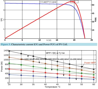
The characteristic curve of a PV cell represents the variation of the current which it produces as a function of the voltage at its terminals, since the short circuit (zero voltage corresponding to the maximum current product) till the open circuit (no current to a maximum voltage across the cell) [5]. In this case, we chose a simple model, requiring only the parameters given by the manufacturer to evoke the influence of meteorological parameters on the maximum power point, the I-V characteristic of this model is shown in Figure 3, and for influences of the conditions meteorological illustrated in Figure 4 and Figure 5: The electrical characteristics of the photovoltaic module that we used were obtained by numerical simulation of the model by Matlab-Simulink software.
The maximum power Pmax suitable for MPP is very susceptible to light as illustrated in Figure 4: when the illumination decreases from 100 W/m2, power Pmax decreases by 10%. With cons, the maximum power
(
Pmax)
decreases little with temperature particularly strong illumination. When the temperature increases from 10˚C to about the ambient temperature and illumination of 1000 W/m2 power Pmax decreased by 4%. [image:3.595.143.488.393.708.2]The optimum voltage Vmpp suitable for MPP varies very little with the illumination and decreases slightly with temperature as illustrated in Figure 5. For illumination of 1000 W/m2 and around ambient temperature (25˚C): when the temperature varies from 10˚C, the voltage ranges from 4.2%. These results show that the vol-tage varies relatively little in the course of the day. Also, it is considered as a first approximation that the optim-al operation of PV generator substantioptim-ally corresponds to operation at constant optimum voltage Vmpp.
Figure 3. Characteristic current I(V) and Power P(V) of PV Cell.
Figure 4. Influence of temperature and illumination on MPP of PV module.
0 5 10 15 20 25
1 2 3 4 I(A ) V (V) I-V and P-V curve
0 5 10 15 20 25
15 30 45 60
P(W)
0 5 10 15 20 25
15 30 45 60
P(W)
0 5 10 15 20 25
15 30 45 60
P(W)
0 5 10 15 20 25
15 30 45 60 P(W) MPP
25 30 35 40 45 50 55 60
0 200 400 600 800 1000 1200 1400 Temperature °C P o w e r (W )
MPP= f(E) at Tj Var
E=800 W/m2
Power MPP
The coefficient of maximum power point MPP and the optimal voltage linking the measured quantities and optimal variables is not always accurately fixed and little vary with time as a function of aging. It depends in particular on temperature and sunlight as illustrated in Figure 4 and Figure 5.
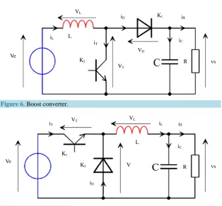
4. Adaptation through of DC-DC Converter
[image:4.595.159.467.261.388.2]The chopper is a DC-DC converter for converting a DC power to a given level of voltage (or current) in a con-tinuous energy to another level of voltage (or current). Use turns out necessary to store solar energy in batteries or to feed a continuous load equivalent circuit of the chopper is represented by Figure 6 and Figure 7 below. Two topologies of bass conversion circuit (DC/DC), choppers are DC-DC static converters for generating a va-riable DC voltage source from a source of fixed voltage. The chopper consists of capacitors, inductors and switches. All of these devices in the ideal case do not consume power, this is the reason why the choppers have good yields. Usually the switch is a MOSFET transistor is a semiconductor device mode (block-saturate), for our work we throw a glance on Boost and Buck converters.
Figure 5. Variation of voltage VMPP according to on the temperature T and illumina-tion E.
Ve
VL
K1 is
vs iD
iT
iL L
K2
VT VD
iC
R
Figure 6. Boost converter.
Ve
VL
K1
is
vs
iD iT
L
K2 VT
V
iC
R iL
Figure 7. BUCK converter.
0 10 20 30 40 50 60 70 80
13 14 15 16 17 18 19
Temperature ( °C )
VM
PP [
V]
VMPP =f(T) at Ej Var
E=200 W/m2
E=1000 W/m2
E=600 W/m2E=800 W/m2
[image:4.595.156.471.418.710.2]4.1. Buck & Boost Converters
The boost converter is known by the name of voltage booster that can be represented by the circuit of Figure 6. The boost converter is characterized by the fact that the output voltage is higher than the input voltage [6]. This is a direct DC-DC converter. The input source is DC-type (inductor in series with a voltage source) and output load is of the type voltage (capacitor in parallel with the resistive load). The switch K1 can be replaced by a transistor since the current is always positive and that the switching should be commanded (the Blocking and priming). A buck converter, or series chopper, is a device that converts a DC voltage into another DC voltage of lower value. The buck converter as illustrated in Figure 7is used in applications where you want to have an output voltage lower than the input voltage [7].
Functioning
For the BOOST, the switch K1 is closed during the αT fraction of the switching period T. The input source provides power to the load R through the inductor L. When transistor is blocked, the diode K2 ensures con-tinuity of the current in the inductor. The energy stored in the inductor is then discharged into the capacitor and the resistance of the load. In steady state, the medium value of the terminal voltage of the inductor is zero, which imposes the following equation:
(
1)
e s
V = −α ⋅V (3)
(
11)
s e
V V
α
= ⋅
− (4)
From Equation (3), the conversion ratio of boost chopper is given in the following form:
( )
(
1)
1 s
e V M
V α
α
= =
− (5)
And for the BUCK converter, the switch K1 is closed during the fraction T of the switching period T. The input source provides an power to the load R through the inductance L. When the Blocking the transistor, the diode K2 ensures continuity of the current in the inductor. The energy stored in the inductor is then discharged into the capacitor and the load resistor. In steady state, the medium value of the terminal voltage of the inductor is zero. The output voltage is given by the following equation:
s L e
V = −V V = ⋅α V (6)
From Equation (6), the conversion ratio of buck chopper is given in the following form:
( )
se V M
V
α = =α (7)
After resolution of equations by Matlab can be shown theFigure 8 illustrates the linear relation between the conversion report and the duty ratio and also to Figure 9 shows the evolution of conversion by the duty cycle ratio.
This is Equation (6) which shows that the buck converter is a step-down voltage because the output voltage of the converter equal to the input voltage by a coefficient which varies in the range [0,1] as illustrated in Figure 8. And Figure 9, in this case it is the Equation (3) shows that the boost converter is a voltage booster.
4.2. Simulation of the Chopper by Matlab Simulink
4.2.1. Chopper SeriesFour demonstrate the role of converters Buck we used Matlab simulation software and we are taking (E=300 V, L=1 H, R=30 Ω). As illustrated in theFigure 10 with the components used and the intercon-nection between them, by Matlab Simulink.
Figure 8. The conversion ratio buck according α.
[image:6.595.97.540.94.625.2]Figure 9. The conversion ratio boost according α.
Figure 10. Block diagram of simulation of Buck converter.
Figure 11. Input voltage to the converter as a function of time.
0 0.1 0.2 0.3 0.4 0.5 0.6 0.7 0.8 0.9 1
0 0.2 0.4 0.6 0.8 1
M=f(alpha)-Buck
Cyclic ratio alpha
C
onv
er
s
ion R
at
io M
0 0.1 0.2 0.3 0.4 0.5 0.6 0.7 0.8 0.9 1
0 5 10 15
M=f(alpha) - Boost
Cyclic ratio alpha
C
onv
er
s
ion R
at
io M
0 0.01 0.02 0.03 0.04 0.05 0.06 0.07 0.08 0.09 0.1
0 50 100 150 200 250
300 Voltage = f(Time)
Time(s)
V
ol
tage(
V
And to give several values of voltage as a function of duty cycle which shows the proportionality between the duty cycle and the input voltage and also to express the role of a Buck in Table 1below shows the variation of the average value of the voltage and current versus duty cycle.
The output voltage of the chopper is not continuous but always be positive. When the time is quite low (fre-quency 100 - 1000 Hz) the load does not “see” the not slots, but the medium value of the voltage. We notice whatever the nature of the charge, we have Vs = ≤0 αU ≤U chopper series is voltage step-down (buck chop-per).
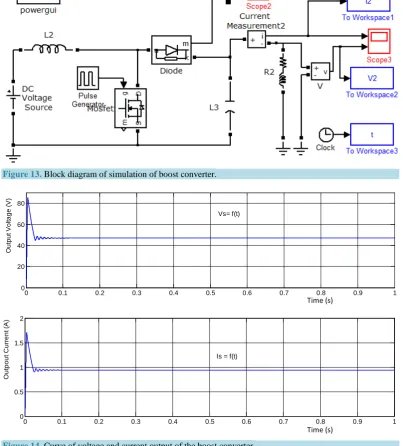
4.2.2. Parallel Chopper
To show the role of converters boost we used Matlab software for the simulation and we take (E=24 V,
3
1 10 H
L= × − , R=50 Ω) as illustrated in Figure 13.
After the results in Figure 14 it is noted that the output voltage Vs ∼47 V is not the same as the input 24 V
e
V ∼ for a duty cycle α =0.5 which expresses the role of boost converter. It is therefore important to play on the cyclic ratio of a share, and on the other hand, although the inductor L dimension, to get a smooth current to the capacitor C and having a desired output voltage.
5. Performance of a Chain Photovoltaic
5.1. Energy Efficiency
We recall the definitions of the different yields and measurement conditions thereof. As a result, the overall yield of the conversion chain reflects all sources of losses over the entire PV chain.
The power received by a panel of area A (m2) is equal to G A⋅ eff.
We will take as a definition reflecting performance the maximum capacity of a GPV and quality of the elec-tron-photon conversion of a solar panel noted ηpv, the performance defined by the equation:
max
eff
pv P
A G
η =
⋅ (8)
max
P : The maximum power delivered by the PV generator.
G: irradiance (W/m2) is defined as the amount of solar electromagnetic energy incident on a surface per unit of time and area.
[image:7.595.88.537.466.625.2]Figure 12. The medium value of the output voltage.
Table 1. The variation of the average value of the voltage and current according α.
α Duty Cycle
α.
0.20 0.30 0.40 0.50
cMoy
U 62 89.1 118 148.5
cMoy
I 1.975 2.970 4.692 4.694
0 0.001 0.002 0.003 0.004 0.005 0.006 0.007 0.008 0.009 0.01
0 50 100 150
Vmoy = f (Time)
Time(s)
V
ol
tage-M
oy
(V
Figure 13. Block diagram of simulation of boost converter.
Time (s)
[image:8.595.112.516.110.557.2]Time (s)
Figure 14. Curve of voltage and current output of the boost converter.
eff
A : Represents the area of the corresponding panel the active part and capable of able to perform of photo-voltaic conversion and not the total area occupied by the solar panel.
The power P effectively delivered by an PV generator depends more on the command used in the converter (MPPT voltage control, direct connection, ...). Performance of the operating point which place we note ηMPPT can measure the effectiveness of the command that is responsible for the control of static converter so that the PV module furnish maximum power.
MPPT
max opt opt
P P
P I V
η = =
⋅ (9)
P is the power available at the terminals of GPV.
opt
V and Iopt are respectively the voltage and current optimal of generator PV.
And performance the converter noted ηconv, which is defined by (10), noting the power Pout delivered at the
0 0.1 0.2 0.3 0.4 0.5 0.6 0.7 0.8 0.9 1
0 20 40 60 80
O
ut
put
V
ol
tage (
V
)
Vs= f(t)
0 0.1 0.2 0.3 0.4 0.5 0.6 0.7 0.8 0.9 1
0 0.5 1 1.5 2
Is = f(t)
O
ut
pout
C
ur
rent
(
A
output the converter
out conv
P P
η = (10)
Unfortunately, more the converter is complex, plus its own performance noted ηconv is low. For the user, the only important overall efficiency η of the entire chain [8] [9]:
MPPT conv
pv
η η η
η= ⋅ ⋅ (11) For these variables must be optimized solar system by intelligent controls (embedded system) to increase the efficiency and effectiveness of our system.
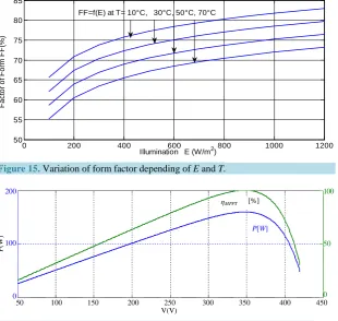
5.2. Form Factor
Called form factor FF, also called factor curve or fill factor, the ratio between the maximum power output Pmax
cell (Iopt, Vopt) and the product of the short-circuit current Isc by the open circuit voltage Voc (that is to say the maximum power an ideal cell). The shape factor indicates the quality of the cell [10]; as it approaches the unit cell is more efficient, it is of the order of 0.7 for efficient cells; and decreases with temperature. It reflects the in-fluence of losses by both parasitic resistances and is defined by:
(
)
max
FF=P Vco⋅Icc (12)
(
)
opt opt
Consequently : FF=V ⋅I Vco⋅Icc (13)
co
V
( )
V : Open circuit voltage.cc
I
( )
A : The current of a short circuit. [image:9.595.161.472.415.709.2]For our system after the simulation of the influence of meteorological parameters on FF and performance are illustrated in the following Figure 15 andFigure 16.
Figure 15. Variation of form factor depending of E and T.
50 100 150 200 250 300 350 400 450 V(V)
0
200 100
50
0
P
(W
)
100
[%]
P[W] ηMPPT
Figure 16.Power available and yield of command for different operating points.
0 200 400 600 800 1000 1200
50 55 60 65 70 75 80 85
Illumination E (W/m2)
Fa
c
to
r o
f Fo
rm
FF
(%
)
When illumination increases the fill factor increases. The fill factor diminishes as the temperature of the de-vice increased. The decrease in FF with the working temperature of the dede-vice outweighs the slight increase in the short circuit current. Finally for having a clearer idea of the origins of losses and yields of each part of a chain of power for a solar system, we presented the definitions of performance and form factor to extract per-formance against weather conditions. In all cases it is necessary to continuously monitor the output voltage of the converter, that is to say either the voltage of the battery charger or the DC bus voltage to an inverter. In addi-tion it is also useful to monitor the battery charge, the battery current measure, then it is easier to maximize the power output of the generator set and the converter because it is this power that is useful and not the extracted panel.
Therefore to increase the efficiency of a solar system must integrate MPPT controls for example knowing that there are different types of algorithms performing the search of maximum power point MPP [11].
6. Conclusion
The performance of the PV generator is evaluated according to the standard conditions (STC): irradiance 1000 W/m2, and Temperature 25˚C. The performance of a PV solar system highly depends on the weather conditions, such as solar radiation, temperature and light, so does the performance of the PV generator degrade with in-creasing temperature, the decrease in intensity and the illumination load variations. To provide energy conti-nuously throughout the year, a PV system must be properly sized and led by intelligent command to monitor MPPT for extracting the maximum energy. And for the simulation of DC-DC converters, we have shown by si-mulation that the average value of the output voltage can be adjusted by varying the duty cycle value. In pers-pective, this work will be continued with a practical realization of MPPT command based microcontroller and a follower by an Arduino board for increasing the efficiency of a solar system to extract the maximum energy.
References
[1] El Alami, M., Habibi, M. and Bri, S. (2013) Parameters Efficiency of Solar Energy. International Journal of Emerging Trends in Engineering and Development—IJETED, 4, 175-186.
[2] Villalva, M.G., Gazoli, J.R. and Filho, E.R. (2009) Comprehensive Approach to Modeling and Simulation of Photo-voltaic Arrays. IEEE Transactions on Power Electronics, 24, 1198-1208.
[3] Hoque, A.K. and Wahid, A. (2000) New Mathematical Model of a Photovoltaic Generator. Journal of Electrical Engi-neering, EE 28, 8p.
[4] El Alami, M., Habibi, M. and Bri, S. (2014) Modelling of Solar System by Newton Raphson Method, MPPT Algo-rithm. European Journal of Scientific Research, EJSR, 120, 264-276.
[5] Yu, G.J., Jung, Y.S., Choi, J.Y., Choy, I., Song, J.H. and Kim, G.S. (2002) A Novel Two-Mode MPPT Control Algo-rithm Based on Comparative Study of Existing AlgoAlgo-rithms. Conference Record of the Twenty-Ninth IEEE Photovoltaic Specialists Conference, 19-24 May 2002, 1531-1534.
[6] Zhou, C., Ridley, R.B. and Lee, F.C. (1990) Design and Analysis of Hysteretic Boost Power Factor Circuit. Annual IEEE Power Electronics Specialists Conference, San Antonio, 800-801. http://dx.doi.org/10.1109/PESC.1990.131271
[7] Prasad, A.R., Ziogas, P.D. and Manias, S. (1992) A New Active Power Factor Correction Method for Single-Phase Buck-Boost AC-DC Converter. Conference Proceedings of Seventh Annual Applied Power Electronics Conference and Exposition,Boston, 23-27 February 1992,814-820.
[8] Hohm, D.P. and Ropp, M.E. (2003) Comparative Study of Maximum Power Point Tracking Algorithms. Progress in Photovoltaics: Research and Applications, 11, 47-62. http://dx.doi.org/10.1002/pip.459
[9] Jain, S. and Agarwal, V. (2007) Comparison of the Performance of Maximum Power Point Tracking Schemes Applied to Single-Stage Grid-Connected Photovoltaic Systems. IET Electric Power Applications, 1, 753-762.
http://dx.doi.org/10.1049/iet-epa:20060475
[10] Nielson, G.N., Okandan, M., Resnick, P., Cruz-Campa, J.L., Pluym, T., Clews, P.J., Steenbergen, E. and Gupta, V.P. (2009) Microscale C-Si (C)PV Cells for Low-Cost Power. 34th IEEE Photovoltaic Specialists Conference (PVSC), Philadelphia, 7-12 June 2009, 1816-1821.