© 2016, IRJET | Impact Factor value: 4.45 | ISO 9001:2008 Certified Journal
| Page 1367
Reduction in Dynamic Power of Digital Circuits by Guarded Evaluation
B. H. K. BHAGATH KUMAR
1K.H.K.RAGHU VAMSI
21
Assistant Professor in E.C.E, Aditya Engineering College,Permanently Affliated to JNTUK A.P, India
2Assistant Professor in E.C.E, Aditya Engineering College, Permanently Affliated to JNTUK A.P, India
Abstract:
In this paper, guarded evaluation is a dynamic power reduction technique by identifying sub circuits inputs and kept constant at specific times during circuit operation. In certain condition, some signals within the digital design are not observable at output. So make such signals as guarded (constant). There by reducing the dynamic power. Here we apply this technique for all digital circuits. The problem here is to find conditions under which a sub circuit input can be held constant with disturbing the main circuit functionally (correctness). Here we propose a solution for discovering the gating inputs based on inverting and non-inverting methods. By including “clock gating” we still reduce the dynamic power and leakage power especially for sequential circuits.Keywords- Guarded evaluation, clock gating,
dynamic power, FPGA.
I.INTRODUCTION
Modern FPGAs are widely used in diverse applications, ranging from communications infrastructure, automotive, to industrial electronics. They enable innovation across a broad spectrum of digital hardware applications, as they reduce product cost, time-to-market, and mitigate risk. However, their use in the mainstream market is often elusive due to their high power consumption. Programmability in FPGAs is achieved through higher transistor counts and larger capacitances, leading to considerably more leakage and dynamic power dissipation compared to ASICs for implementing a given function. Guarded evaluation
seeks to reduce net switching activities by modifying the circuit network. In particular, the approach taken is to eliminate toggles on certain internal signals of a circuit when such toggles are guaranteed to not propagate to overall circuit outputs. Unlike guarded evaluation in ASICs, this involves adding additional circuitry (increasing area and cost), our approach uses unused circuitry that is already available in the FPGA fabric, making it less expensive from the area perspective. Specifically, input pins on LUTs are frequently not fully utilized in modern designs, and we use the available free inputs on LUTs for guarded evaluation. This implies that we do not add in any additional LUTs when implementing guarding, but rather only add a minimal amount of extra connections into the network. In our approach, identifying the
conditions under which a given signal can be guarded is accomplished by analyzing properties of the logic synthesis network, which is an And-Inverter Graph (AIG). In particular, we show that the presence of “non-inverting” and “partial non-“non-inverting” paths in the AIG can be used to drive the discovery of guarding opportunities. This structural-based approach to determining guarding opportunities proves to be very efficient. Finally, we consider the introduction of different types of guarding logic (as opposed to transparent latches which are used for ASICs) to reduce unnecessary transient switching.
© 2016, IRJET | Impact Factor value: 4.45 | ISO 9001:2008 Certified Journal
| Page 1368
change state by signals applied to one or more controlinputs and will have one or two outputs. It is the basic storage element in
sequential logic. Flip-flops and
latches are a fundamental building block ofdigital
electronics
systems used in computers, communications, and many other types of systems. Flip-flops and latches are used as data storage elements. Such data storage can be used for storage of state, and such a circuit is described as sequential logic. When used in afinite-state machine, the output and next state depend
not only on its current input, but also on its current state (and hence, previous inputs). It can also be used for counting of pulses, and for synchronizing variably-timed input signals to some reference timing signal. Flip-flops can be either simple (transparent or opaque) or clocked (synchronous or edge-triggered), the simple ones are commonly called latches.Logic synthesis is the process of converting a high-level description of design into an optimized gate-high-level representation [1]. Logic synthesis uses a standard cell library which have simple cells, such as basic logic gates like and, or, and nor, or macro cells, such as adder, muxes, memory, and flip-flops. Standard cells put together are called technology library. Normally the technology library is known by the transistor size. A circuit description is written in Hardware Description Language (HDL) such as Verilog.
II.BACKGROUND
A. Guarded Evaluation
Guarded evaluation comprises first identifying an internal Signal whose value does not propagate to circuit outputs under certain conditions. A straight forward example is an AND gate with two input signals, A and B. Values on signal A do not Propagate to circuit outputs when B is logic-0 (the condition). Thus, toggles on A are
an unnecessary waste of power when B is logic-0. Having found a signal and condition, guarded evaluation then modifies the circuit to eliminate the toggles on the signal when the condition is true the inputs to the circuitry that produce A can be held at a constant value (guarded) when the condition is true, reducing dynamic power. The computationally difficult aspect of the process is in finding signals (such as A) and computing the conditions under which they are not observable, as these steps depend on an analysis of the circuit’s logic functionality
.
Fig1(a). Before guarded evaluation
© 2016, IRJET | Impact Factor value: 4.45 | ISO 9001:2008 Certified Journal
| Page 1369
We proposed using guarded evaluation in ASICs toattack both leakage and dynamic power [2]. The guarding signals were used to drive the gate terminals of NMOS sleep transistors incorporated into CMOS gate pull-down networks, putting sub circuits into low-leakage states when their outputs were not needed. Their approach produced encouraging power reduction results by exploiting select signals on steering elements (multiplexers) to serve as guarding signals and is therefore limited to specific types of circuits.
B. Methods:
1).Gating Inputs and Non-Inverting AIG Paths:
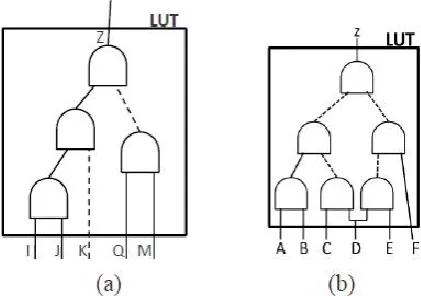
Fig. 3(a) gives an example of a LUT and Portion of a covered AIG. Examine the AIG path from the input I to the root gate of the AIG, Z. The path comprises a sequence of AND gates with none of the path edges being complemented. Recall that the output of an AND gate is logic- 0 when either of its inputs is logic-0. For the path from I to Z, when I is logic-0, the output of each AND the corresponding gate along the path will be logic-0, ultimately producing logic-0 on the LUT output. We therefore conclude that I is a gating input to the LUT. The LUT in Fig 3(a), in fact, has three gating inputs, I, J, and K. Input J is the same form as input I in that there exists a path of AND gates from J to root gate Z and none of the edges along the path are inverted.
For input K, the “frontier” edge crossing into the LUT is inverted, however, aside from this frontier edge, the remaining edges along the path from K to the root node Z are “true” edges. This means that when K is logic-1, the output of the AND gate it drives will be logic-0, eventually making the LUT’s output signal Z logic-0. K is indeed a gating input, though it is K’s logic-1 state (rather than its logic-0 state) that causes the LUT output to be logic-0. In contrast with inputs I, J and K, LUT inputs Q and M are not gating inputs to the LUT as
neither logic state of these inputs causes the LUT output to be logic-0.
2).Trimming Inputs and Partial Non-Inverting AIG Paths
More opportunities for guarding can be found by considering trimming inputs in addition to gating inputs in Fig. 3(a). There is no non-inverting path from any LUT input to the LUT output. However, we can observe that a logic-0 on input A will still force the output on some AND gates to be logic-0 as its value propagates towards Z. We can identify the AND gate that drives the first inverted edge on the path from A to Z and, subsequently, find the fan-out-free cone rooted at the identified AND gate; the set of LUT inputs to this fan-out-free cone (excluding A) can be trimmed by A when A is a logic-0. In this example, this means inputs B and C can be trimmed when input A is a logic-0. Note that input D cannot be trimmed since it is not in the fan-out free fan-in cone of the affected AND gates. Input F can be used to
trim input E (but not input D) when F is a logic-0.
Fig 2.(a). Identifying gating inputs on LUTs using noninverting paths;
[image:3.595.326.537.470.618.2]© 2016, IRJET | Impact Factor value: 4.45 | ISO 9001:2008 Certified Journal
| Page 1370
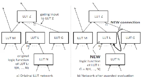
Fig 3. Guarded evaluation for FPGAsFig. 4(a) illustrates how gating and trimming inputs to LUTs can be applied for guarded evaluation. Without loss of generality, assume that logic-0 is the state of the gating input, G, that causes LUT Z’s output to be logic-0.When G is logic- 0, Z is also logic-0, and any toggles on the other inputs of Z are guaranteed not to propagate through Z to circuit outputs. Similarly, if G is a trimming input of, say, input L (i.e., a logic-0 on G blocks toggles on signal L from propagating to signal Z), then L can also be guarded by signal G. Since L’s single fan-out is to Z, L’s output value will not affect overall circuit outputs when G is logic-0. Toggles that occur in computing L’s output when G is logic-0 are an unnecessary waste of dynamic power.
In Fig. 4(a), L is a candidate for guarded evaluation by Signal G. If LUT L has a free input, we modify the mapped network by attaching G to L, and then modifying L’s logic functionality as shown in Fig. 4(b). The question is how to modify L’s logic functionality. In [6], logic functions were modified to force the LUT output to a logic-0 when guarded. Consider the case where the output of LUT L in Fig. 4(b) was logic-1 the instant prior to guarding. If it was guarded using a logical AND of its previous function and signal G, then the gate would induce one additional toggle from logic-1 to logic-0. Hence, the static probability of the guarded signal is examined prior to inserting the guarding logic to avoid such additional (and
© 2016, IRJET | Impact Factor value: 4.45 | ISO 9001:2008 Certified Journal
| Page 1371
I. CLOCKGATING
In today’s semiconductor designs, lower power consumption is mandatory for mobile and handheld applications for longer battery life and even networking or storage devices for low carbon footprint requirements. Clock power consumes 60-70 percent of total chip power and is expected to significantly increase in the next generation of designs at 45nm and below. This is due to the fact that power is directly proportional to voltage and the frequency of the clock as shown in the following equation.
Power=Capacitance * (Voltage) 2 * (Frequency)
Clock gating is a popular technique used in many synchronous circuits for reducing dynamic power
dissipation
[4]. Clock gating saves power by adding more logic to a circuit to prune the clock tree. Pruning the clock disables portions of the circuitry so that the flip-flops in them do not have to switch states. Switching states consumes power. When not being switched, the switching power consumption goes to zero, and only leakage currents are incurred load to node X causes speed and power performance degradation [7]. Clock gating works by taking the enable conditions attached to registers, and uses them to gate the clocks. Therefore it is imperative that a design must contain these enable conditions in order to use and benefit from clock gating [5]. This clock gating process can also save significant die area as well as power, since it removes large numbers of muxes and replaces them with clock gating logic.A. HOW TO IMPLEMENT CLOCK GATING
When there is no activity at a register “data” input, there is no need to clock the register and hence the “clock” can be gated to switch it off. If the clock feeds a bank of registers, an “enable” signal can be used to gate the clock, which is called the “clock gating enable”.
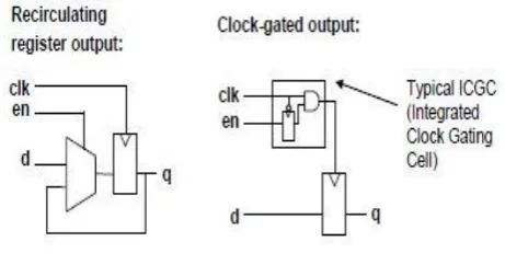
Fig 4.(a). Feedback mux Fig 4.(b). Integrated clock gating
This clock gating logic is generally in the form of "Integrated clock gating" (ICG) cells. However, note that the clock gating logic will change the clock tree structure, since the clock gating logic will sit in the clock tree [6]. As shown in Figure 4.(a), when an “explicit” clock enable exists in the RTL code, synthesis tools may choose between two possible implementations. The implementation as shown in Figure 1a is a “re-circulating register” implementation, where the enable is used to either select a new data value or re-circulate the previous data value.
[image:5.595.319.550.239.365.2]© 2016, IRJET | Impact Factor value: 4.45 | ISO 9001:2008 Certified Journal
| Page 1372
B. CLOCK GATING USING ASIC DESIGN
Fig 4. Clock gating in Asic Design
Fig. 4 Any RTL modifications to improve clock gating will result in functional changes to the design (since the registers will now hold different values) which need to be verified. Sequential clock gating is the process of extracting/propagating the enable conditions to the upstream/downstream sequential elements, so that additional registers can be clock gated. Although asynchronous circuits by definition do not have a "clock", the term perfect clock gating is used to illustrate how various clock gating techniques are simply approximations of the data-dependent behavior exhibited by asynchronous circuitry [8]. As the granularity on which you gate the clock of a synchronous circuit approaches zero, the power consumption of that circuit approaches that of an asynchronous circuit: the circuit only generates logic transitions when it is actively computing.
II. RTL Power Estimation Flow
Early power estimation at RTL can help the designer to quickly explore different architectures like replacing large memories with smaller memories or register files and find power bugs early in the design before it is found too late at the gate-level where synthesis and place and
route steps will have to be iterated to meet the required power budget for the design.
[image:6.595.38.270.138.276.2]Fig 5. RTL Power Estimation Flow
© 2016, IRJET | Impact Factor value: 4.45 | ISO 9001:2008 Certified Journal
| Page 1373
III.
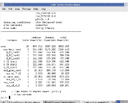
SIMULATION RESULTSThe simulation results are for the asic designs before applying the guarded evaluation and after applying both guarded as well as clock gating. We have observed the dynamic power and the leakage power is reduced after applying the techniques.. The simulation results are schematic circuits designed in Questasim (10.2a) Tool and the power calculations are carried out in the CADENCE RTL COMPLIER Tool. The results are as shown in Fig 6(a). Before Asic Design Schematic in Questasim Tool, Fig 6(b). Before Asic Design Wave Form in Questasim Tool, Fig 6(c). Before Asic Design Schematic in Precision Tool, Fig 6(d). Before Asic Design RTL Power in, Fig 7(a). Clock gating Asic Design Schematic in Questasim Tool, Fig 7(b). Clock gating Asic Design Wave Form in Questasim Tool, Fig 7(c). Clock gating Asic Design Schematic in Precision Tool, Fig 7(d). Clock gating Asic Design RTL Power in Cadence Tool.
Fig 6(a). Before Asic Design Schematic in Questasim Tool
Fig 6(b). Before Asic Design Wave Form in Questasim Tool
Fig 6(c). Before Asic Design Schematic in Precision Tool
[image:7.595.311.531.63.247.2] [image:7.595.316.526.306.451.2] [image:7.595.43.266.462.624.2] [image:7.595.315.526.524.691.2]© 2016, IRJET | Impact Factor value: 4.45 | ISO 9001:2008 Certified Journal
| Page 1374
Fig 7(a). Clock gating Asic Design Schematic in Questasim ToolFig 7(b). Clock gating Asic Design Wave Form in Questasim Tool
Fig 7(c). Clock gating Asic Design Schematic in Precision Tool
Fig 7(d). Clock gating Asic Design RTL Power in Cadence Tool
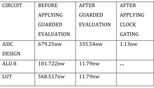
TABLE1: Power reduction results for different circuits
CIRCUIT BEFORE
APPLYING GUARDED EVALUATION
AFTER GUARDED EVALUATION
AFTER APPLYING CLOCK GATING ASIC
DESIGN
679.25nw 335.54nw 1.13nw
ALU 8 101.722nw 11.79nw
--
[image:8.595.36.259.97.280.2] [image:8.595.315.592.316.503.2] [image:8.595.36.270.340.530.2] [image:8.595.312.565.550.695.2]© 2016, IRJET | Impact Factor value: 4.45 | ISO 9001:2008 Certified Journal
| Page 1375
IV. CONCLUSIONSIn this paper, the various digital designs and especially sequential circuits are used .Main aim is reducing the dynamic power and leakage power. Guarded evaluation reduces dynamic power by identifying sub-circuits whose inputs can be held constant at certain times during circuit operation, eliminating toggles within the sub circuits. Numerical results demonstrate the efficacy of our proposed techniques and show that guarded evaluation is effective for FPGA designs. We have proposed a structural technique to Identify guarding candidates based on the ideas of non inverting and partial inverting paths; the use of partial non-inverting paths was demonstrated to significantly improve the availability of guarding options and, in turn, improve the reduction in both total reduction in total switching activity and reduction in total dynamic power dissipation. Finally we got a better result by applying clock gating to sequential circuits. It reduces both dynamic and leakage power.
REFERRENCES
[1] S. Jang, K. Chung, A. Mishchenko, and R. Brayton, “A power optimization toolbox for logic synthesis and mapping,” in Proc. IEEE Int. Workshop Logic
[2] V. Tiwari, S. Malik, and P. Ashar, “Guarded evaluation: Pushing power management to logic synthesis/design,” IEEE Trans. Computer.-Aided Des., vol.
17, no. 10, pp. 1051–1060, Oct. 1998.
[3] J. Anderson and Q.Wang, “Improving logic density through synthesis-inspired architecture,” in Proc. IEEE Int. Conf. Field-Programmable Logic Applicant.
Aug.–Sep. 2009, pp. 105–111.
[4] A. Mishchenko. (2009). ABC: A System for Sequential Synthesis and Verification[Online].
[5] Clock-Gating and Its Application to Low Power Design of Sequential Circuits Qing WU Department of Electrical Engineering-Systems, University of Southern California Los Angeles, CA 90089, USA.
Available: http://www.eecs.berkeley.edu/∼alanmi/abc
[6] Altera Corporation. (2009). Quartus-II University Interface Program [Online].
Available:http://www.altera.com/education/univ/research unv-quip.html
[7] A. Abdollahi, M. Pedram, F. Fallah, and I. Ghosh. Precomputationbas Guarding for dynamic and leakage power reduction. In IEEE Int’l
Conf. on Computer Design, pages 90–97, 2003.
[8] J. Anderson and C. Ravishankar. FPGA power reduction by guarded evaluation. In ACM/SIGDA Int’l Symp. on Field Programmable Gate
Arrays, pages 157–166, 2010.
[9] D. Howland and R. Tessier. RTL dynamic power optimization for FPGAs. In IEEE Midwest Symp. On Circuits and Systems, pages 714– 717, 2008.
[10] K. Poon, A. Yan, and S. Wilton. A flexible power model for
FPGAs.In Int’l Conf. on Field-Programmable Logic and Applications, pages
312–321, 2002.
[11] L. Shang, A. Kaviani, and K. Bathala. Dynamic power consumption ofthe Virtex-II FPGA family. In ACM Int’l Symp. on Field Programmable
Gate Arrays, 2002.
BIOGRAPHY
B.H.K. Bhagat Kumar*1 received the
M.Tech. Degree in Embedded System from the Pragati engineering college affiliated to JNTU Kakinada in 2013. He is currently working as an Assistant Professor in the Department of Electronics & communication Engineering, Aditya Engineering College, Surampalem. His research interests are VLSI & Embedded real time operating system in relation with power consume and defilation
K.H.K.Raghu Vamsi*2 received the