interactions in a metal-molecule-metal (M-M-M) structure. In an M-M-M system, the electronic function is a property of the structure and can be characterized through I/V measurements. The contact between the metals and the molecule was obtained by gold nanogaps (with a dimension of less than 10 nm), produced with the electromigration technique. The nanogap fabrication was controlled by a custom hardware and the related software system. The studies were carried out through experiments and simulations of organic molecules, in particular oligothiophenes.
1 Introduction
Electrical nanogap devices are emerging because of their possibility to be the building blocks for connecting [1], analyzing [2], and using molecules, and so for imple-menting nano-metric electronic devices [3]. The main advantage of these systems is, in general, the ability to measure and to transduce events of specific molecules into useful electrical signals [4]. As a consequence, nanogaps have nowadays a high level of interest in research. There are a lot of techniques for obtaining nanogaps, but a process to totally control the gap size has not been found yet. Electromigration effect is the simplest technique useful for obtaining the break of the two terminals structures where the nanogap is built [5,6]. Electro-induced break junction (EIBJ) can generate an instantaneous and random break, but to obtain reproducible and stable devices it is very important to control the width of the nanogap [7,8]. For this reason, the quantity of current used to stimulate the electromi-gration effect must be controlled with a custom feed-back circuit that manages all the fabrication steps. The authors defined a method for producing nanogaps inside gold structures, and the controlled use of the electromi-gration enabled to build gaps under ten nanometers.
2 Experimental section
2.1 Realization of the chip
The electromigration is mainly dominated by the cur-rent density [9] and by the temperature of the wire [10].
Both these quantities can be controlled by a proper geo-metry of the probe [11] and by the applied voltage waveform [12]. Using electromigration as technique for creating nanogaps, the wire has to have optimized geo-metries to facilitate the phenomenon and make it more controllable. From this point, to avoid a too high input current, it is necessary to have a small section of the wire [11]; moreover, if the section of the wire is too small, the thermal conductance decreases and the tem-perature of the wire tends to become excessive, leading to the melting of the wire.
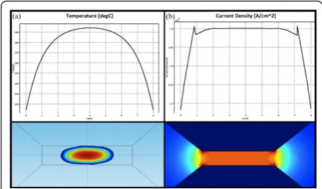
For these reasons, it is fundamental to have a model that can simulate the behavior of the physical phenom-ena during the electromigration. In particular, it is inter-esting to know and to anticipate the temperature inside the gold wire and for this it is necessary to model the geometry of the probe with a software simulation tool. The objective is therefore to achieve a wire section as small as possible, to trigger the electromigration also at lower current, obtaining a better control and a more regular shape. Figure 1a shows the geometry of our probe described in Comsol Multi-physics, while Figure 1b shows the single wire. To evaluate the temperature behavior during the voltage application, we performed a large number of simulations using different values of wire length, keeping in mind that there is a lower limit for the length of the wire that will allow electromigra-tion to occur (the Blech length [13-15]). Figure 1c shows the best parameters for generating a temperature profile quite sharp in a way that should be possible to focus the electromigration phenomenon in the center of the wire. The temperature profile along wire length was * Correspondence: [email protected]
1Department of Electronics, Corso Duca degli Abruzzi 24, 10129 Turin, Italy
Full list of author information is available at the end of the article
modeled with the equations:
Q=ρCp∂
T
∂t − ∇(K∇T) (1)
Q=σ|∇V|2 (2)
J=σ∇V (3)
Equation (1) is the law of conservation of energy:Qis
the power transferred to a point,ris the mass volume
density,Cpis the heat capacity,Tis the temperature,tis the time andKis the thermal conductivity. Equation (2) gives the power dissipation (Joule effect):sis the electri-cal conductivity andVis the electrical potential. Finally, Equation (3) is the Ohm’s law in local form:Jis the cur-rent density. All the equations are related to an infinitesi-mal point of space. Comsol uses the nodes of the mesh geometry to make a spatial sampling and integrates the equations in the volume using the nodes as points of integration: if the sampling is quite dense, the error is negligible. As result we have obtained the plot shown in Figure 2a that represents the temperature variation in the wire length. The geometry created also allows a uniform distribution of current density (Figure 2b).
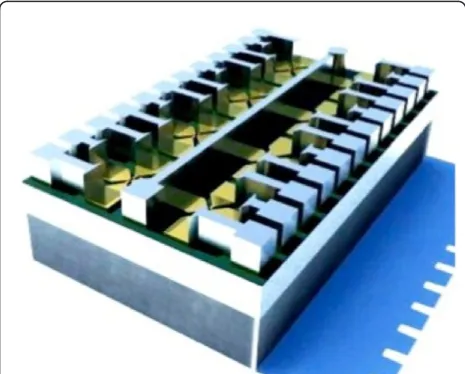
For having a useful platform where to produce the nanogaps, a silicon chip was realized, containing eight gold probes as shown in Figure 3b, each of these con-nectable by bonding. In this way, it is possible to realize on the same chip eight nanogap structures, and each one is independent, so an high number of measure-ments is individually achievable. The final dimension of
the chip is 2.4 × 4.1 mm, giving the possibility to insert it in heads of instruments as a cryostat or FESEM/ AFM/STM microscopes, for doing for example mea-surement in vacuum and at very low temperatures. The chip is also ready to be wire bonded to a PCB (Figure 3a). It is possible to perform wet analysis too, for mole-cule characterizations, just spinning on the chip the solution that has to be measured. Obviously molecules in solutions must have some suitable sites for bonding with gold, such as thiol groups, in this way it is possible to obtain the desired M-M-M structure.
The realization of the chip starts from a silicon wafer capped by 200 nm of SiO2; the wafer is, then, inserted
[image:2.595.57.290.88.264.2]in a plasma oxygen machine for increasing the oxygen atoms concentration on the surface. Hydroxylation pro-cess is developed with a piranha solution, and so, after rinsing and drying, the surface of the wafer exposes -OH groups, fundamental for the anchoring of the organic compound that is evaporated on. In fact, to Figure 1Comsol model of the probe.(a)Geometry of the probe;
(b)single wire level;(c)best parameters for generating a sharp temperature profile: wire length l_wire = 8μm; wire width s_wire = 2μm; wire thickness au_z = 25 nm; substrate thickness bios_z = 200 nm.
[image:2.595.304.538.89.226.2]Figure 2Results of the electrothermal simulation made with Comsol.(a)Temperature profile;(b)current density profile.
[image:2.595.307.536.513.668.2]solution. A second photolithographic process is per-formed through a second mask that allows the
realiza-tion of the chip’s pads, built with a thin layer of
titanium of 100 nm and an aluminum layer of 700 nm (see Figure 4).
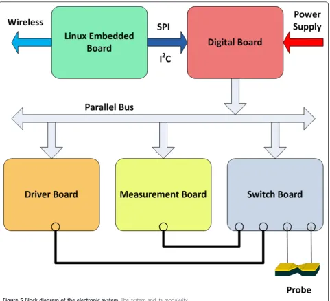
The custom hardware
To control the experiments, a custom electronic board, connected to a Linux-embedded system, has been
rea-lized. To provide the current density of 108A/cm2,
needed for the activation of the electromigration pro-cess, the circuit must be able to supply a current of at least 50 mA, because of the dimensions of realized geo-metries. The front-end must also be able to measure the real time current flowing in the wire, to evaluate resis-tance variations, from hundreds of mA (when the cur-rent is high and the break is not yet created) to some pA (for measuring the tunnel current inside the nano-gap). The block diagram of the system is showed in Fig-ure 5, where it is possible to see that the gold probe is connected to the circuit that receives the signal from the embedded Linux (analog input) and generates the desired current for inducing the electromigration. The
order to measure a wide range of currents, and an ana-log-to-digital converter; aswitch boardto allow the con-nection of external instrumentation; a digital boardthat provides electrical power supplies and the bus connec-tion between all boards. The embedded Linux system is built with a real-time custom kernel, so that the electro-nic components of the other boards are driven in a deterministic way. We have developed a wireless con-nection between this board and a host computer for sending the experimental data. This solution allows also the use of the system in chambers where a wire inter-connection can create difficulties.
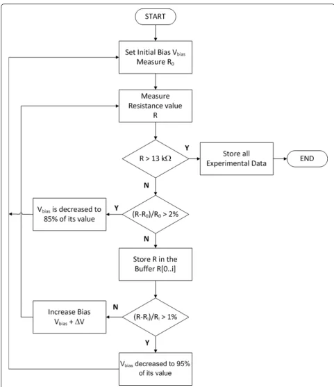
The custom algorithm
Nanogaps are produced using a specific algorithm, custo-mized for an optimal nanogap fabrication and with sev-eral goals: current management, feedback controlled breaking, temperature control for avoiding the thermal runaway. A simplified schematic of the process flow is reported in Figure 6. The software controls the voltage Vbiasapplied to the probe and stops when the resistance
exceeds the value of 13kΩ, that means that the nanogap is produced. In fact this resistance value is about the inverse of the quantum conductance 2e2/h= 77.6μSand represents the conductance of a single atom of gold placed between two electrodes [23]. As it is possible to see always in Figure 6, there are two feedback mechan-isms. The first one performs an absolute control over the initial resistanceR0, and when (R-R0)/R0>0.02 theVbias
is set to the 85% of its value; this is done for controlling the temperature of the wire and for preventing melting and surface tension effects, that can be the cause of much larger gaps and gold island formation [18-20]. The second mechanism performs a check of the resistance value relative to a circular buffer of n samples, when (R -Ri)/Ri>0.01, withRithe average of the lastisamples, the Vbias is decreased to the 95% of its value. The second
[image:3.595.57.290.513.700.2]feedback mechanism performs a check of the resistance in order to control the electromigration effect: the increase of the resistance is no longer linear as in the Joule Heating, but exponential, and we need to promptly react to stop the phenomenon. We also noted in many experiments performed by us, that, after the activation of Figure 4Chip structure representation. 3D representation of the
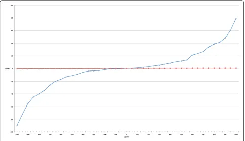
the feedback, the resistance value decreases due to the acceleration of the grain growth by Joule heating of the wire [24]. In this case, the first mechanism becomes use-less and then the process is controlled only by the second one. Figure 7 shows the probe resistance as a function of the voltage applied: when the temperature increases, the resistance of the wire tends to increase too.
The higher resistance causes a current reduction, but increasing the voltage in this case creates a mechanism by which the current flow tends to be constant. In fact the first increase in resistance (linear growth) is only due to this heat effect, but, when the temperature reaches high values and the current density is near to
108 A/cm2, the electromigration starts (exponential
growth) and the structure begins to change.
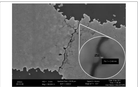
The experimental time of electromigration has been estimated to be about 50-60 min. All the experimental data obtained by the electromigration tests are stored in an internal database in the Linux board, but on the host computer too, that collects information through the wireless connection. This makes possible to generate very accurate statistics. To evaluate the outcome of our experiments, we performed the analysis of gap widths with a FESEM microscope. Example of a fabricated nanogap is shown in Figure 8.
3 Results
The method used to fabricate nanogaps, through these
[image:4.595.59.541.87.525.2]is interesting to observe that the gap has an almost con-stant width for a relative long path. Analyzing the experimental results, fabricated nanogaps show an aver-age dimension of less than 10 nm. Statistical analysis
[image:5.595.55.537.84.642.2]about the final dimension of the gaps confirm that the authors are now able to create nanogaps under 10 nm with an high reproducibility (Figure 9), in fact about the 80% of the nanogaps are under 10 nm.
Figure 7Monitoring plot of the probe resistance. R/V plot of an EIBJ experiment.
[image:6.595.57.539.393.698.2]To evaluate the use of nanogaps as electrodes for molecular electronics, a solution of oligothiophenes molecules (2,2’:5’,2":5”,2"’-bis-quaterthiophene) in Tetra-HydroFuran (THF) has been deposited using the method of spin coating. The choice of this type of mole-cules is due to the presence of a sulfur atom in the aro-matic ring: it binds easily to the gold of the nanogap electrodes. After the insertion in the nanogaps, the
between the molecule and the electrodes are not per-fectly symmetric [30-32].
The molecular length plays a key role in the electrical conduction.
Experiments have found that the conductance G
decreases exponentially with molecular length L [33]
and can be described by
G=Ae−βL (4)
where Ais a constant and bis a decay constant
vary-ing between 0.09 and 0.16 Å-1 for the oligothiophenes
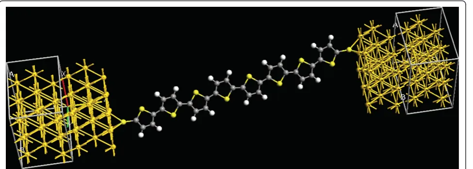
[image:7.595.58.291.88.251.2][28,29]. Figure 11 shows an ab initio simulation of the molecule placed between the electrodes where the mole-cule orientation was performed with the software Gaus-sian 09. Different orientations are possible, but less Figure 9Plot of the distribution of the nanogap dimension.
Statistical dispersion of nanogap dimensions, 80% of them are under 10 nm.
[image:7.595.57.541.417.695.2]probable. Moreover, our simulations show a variation of the current less than 30% respect to the optimized case, keeping the same shape of the I/V curve.
4 Conclusions
A system composed by a software interface and an elec-tronic control circuit for the nanogap realization has been implemented, and all the technological steps for arriving at the final nanogap production has been pre-sented in this study. The probe geometries were opti-mized through electrothermal simulations performed with the COMSOL Multi-physics software. The method applied demonstrated the possibility to build nanogaps under 3 nm with controlled feedback, having a good sta-tistical yield with about the 80% of the nanogaps below 10 nm (Figure 9). In the experimental phase an oli-gothiophene molecule was successfully inserted in the nanogap, producing a first Metal-Molecule-Metal sys-tem, and it was characterized by current-voltage (Figure 10) measurements, taking into account that the coupling between metal and molecule plays a key role. Future study will be focused on the optimization of the system for the realization of integrated molecular devices.
Acknowledgements
The authors would like to acknowledge Dr. Valentina Cauda for the precious advices about chemistry, Dr. Salvatore Guastella for the FESEM microscope characterizations, Dr. Dario Trimarchi and Dr. Davide Daprà for the electronic system design. They want to acknowledge too the group of Prof. Mucci at University of Modena for the synthesis of the oligothiophene molecules.
Author details
1Department of Electronics, Corso Duca degli Abruzzi 24, 10129 Turin, Italy 2Italian Institute of Technology, IIT@Polito Center, Corso Trento 21, Turin, Italy
Authors’contributions
PM made the electronic system, the EIBJ experiments, developed the RT kernel and integrated the algorithm into the software. AD realized the chip
in clean room. IR performed the electrothermal simulation. DD, GP and PC designed the experimental idea and gave technical background and support concerning the field of study. All authors read and approved the final manuscript.
Competing interests
The authors declare that they have no competing interests.
Received: 28 November 2011 Accepted: 9 February 2012 Published: 9 February 2012
References
1. Tour JM:Molecular electronics. synthesis and testing of components.Acc Chem Res2000,33(11):791-804.
2. Shiigi H, Tokonami S, Yakabe H, Nagaoka T:Label-free electronic detection of dna-hybridization on nanogapped gold particle film.J Am Chem Soc (JACS)2005,127:3280-3281.
3. Ventra MD, Pantelides ST, Lang ND:The benzene molecule as a molecular resonant-tunneling transistor.Appl Phys Lett2000,76(23):3448-3450. 4. Yi M, Jeong KH, Lee LP:Theoretical and experimental study towards a
nanogap dielectric biosensor.Biosen Bioelectron2005,20:1320-1326. 5. Morpurgo AF, Marcusa CM, Robinson DB:Controlled fabrication of
metallic electrodes with atomic separation.Appl Phys Lett1999,
74(14):2084-2086.
6. Park H, Lim A, Alivisatos A:Fabrication of metallic electrodes with nanometer separation by electromigration.Appl Phys Lett1999,
75(2):301-303.
7. Shih VCY, Zheng S, Chang A, Tai YC:Nanometer gaps by feedback-controlled electromigration.The 12th International Conference on Solid State Sensors, Actuators and Microsystems, Boston2003,2:1530-1533. 8. Wu ZM, Steinacher R, Calame S, van der Molen SJ, Schnenbergera C:
Feedback controlled electromigration in four-terminal nanojunctions.
Appl Phys Lett2007,91, 053 118-1-053 118-3.
9. Pierce DG, Brusius PG:Electromigration: A review.Microelectron Reliab 1997,37(7):1053-1072.
10. Trouwborst ML, van der Molen SJ, van Wees BJ:The role of Joule heating in the formation of nanogaps by electromigration.J Appl Phys2006,
99(11):114316-1-114316-7.
11. Durkan C, Schneider MA, Welland M:Analysis of failure mechanisms in electrically stressed gold nanowires.J Appl Phys1999,99:1280-1286. 12. Hadeed FO, Durkan C:Controlled fabrication of 1-2 nm nanogaps by
electromigration in Au and Au/Pd nanowires.Appl Phys Lett2007,
91:123120.
13. Blech IA:Electromigration in thin aluminum films on titanium nitride.J Appl Phys1976,47(4):1203-1208.
[image:8.595.58.546.89.263.2]14. Blech IA, Herring C:Stress generation by electromigration.Appl Phys Lett 1976,29(3):131-133.
electromigrated gold break junctions.Nano Lett2005,5(9):1685-1689. 21. Esen G, Fuhrer MS:Temperature control of electromigration to form gold
nanogap junctions.Appl Phys Lett2005,87:263101.
22. van der Zant HSJ:Molecular three-terminal devices: fabrication and measurements.Faraday Discuss2006,131:347-356.
23. Datta S:An atomistic view of electrical resistance.InQuantum Transport: Atom to TransistorEdited by: Cambridge University Press: Cambridge University Press, New York 2005,1:1-30.
24. Chengxiang X, Jung YK, Reginald MP:Reconnectable sub 5 nm nanogaps in ultralong gold nanowires.Nano Lett2009,9:2133-2138.
25. Zahid F, Paulsson M, Datta S:Electrical Conduction through Molecules.In Advanced Semiconductors and Organic Nano-Techniques.Edited by: Morkoc H. Waltham, Massachusetts: Academic Press (Elsevier); 2003:.
26. Salomon A, Cahen D, Lindsay S, Tomfohr J, Engelkes VB, Frisbie CD:
Comparison of electronic transport measurements on organic molecules.Adv Mater2003,15(22):1881-1890.
27. P BJ:Molecular electronics: a rewiew of Metal-Molecule-Metal junctions.
Lecture Notes Phys2001,579:105-124.
28. Yamada R, Kumazawa H, Noutoshi T, Tanaka S, Tada H:Electrical conductance of oligothiophene molecular wires.Nano Lett2008,
8:1237-1240.
29. Yamada R, Kumazawa H, Tanaka S, Tada H:Electrical resistance of long oligothiophene molecules.Appl Phys Express2009,2:025002. 30. Mujica V, Ratner M:Molecular Conductance Junctions: A Theory and
Modeling Progress Report.InHandbook of Nanoscience, Engineering, and Technology. Volume 12.Edited by: WA Goddard, DW Brenner SE Lyshevski, and GJ Iafrate, Boca Raton, FL. USA: Taylor 2002:1-27.
31. Speyer G, Akis R, Ferry DK:Complexities of the molecular conductance problem.Nano and Molecular Electronics HandbookBoca Raton, FL, USA: Taylor & Francis Group LLC, CRC Press; 2007.
32. Chen F, Hihath J, Huang Z, Li X, Tao NJ:Measurement of Single-Molecule Conductance.Annu Rev Phys Chem2007,58:535-564.
33. Tao NJ:Electron transport in molecular junctions.Nat Nanotechnol2006,
1:173-181.
doi:10.1186/1556-276X-7-113
Cite this article as:Mottoet al.:Nanogap structures for molecular nanoelectronics.Nanoscale Research Letters20127:113.
Submit your manuscript to a
journal and benefi t from:
7 Convenient online submission
7 Rigorous peer review
7 Immediate publication on acceptance
7 Open access: articles freely available online
7 High visibility within the fi eld
7 Retaining the copyright to your article